EP0285798A2 - Dispositif de test électrique du fonctionnement de rangées de fils électriques, en particulier pour cartes de circuit - Google Patents
Dispositif de test électrique du fonctionnement de rangées de fils électriques, en particulier pour cartes de circuit Download PDFInfo
- Publication number
- EP0285798A2 EP0285798A2 EP88103017A EP88103017A EP0285798A2 EP 0285798 A2 EP0285798 A2 EP 0285798A2 EP 88103017 A EP88103017 A EP 88103017A EP 88103017 A EP88103017 A EP 88103017A EP 0285798 A2 EP0285798 A2 EP 0285798A2
- Authority
- EP
- European Patent Office
- Prior art keywords
- gas discharge
- photoconductors
- light
- discharge channels
- photoresistors
- Prior art date
- Legal status (The legal status is an assumption and is not a legal conclusion. Google has not performed a legal analysis and makes no representation as to the accuracy of the status listed.)
- Withdrawn
Links
Images


Classifications
-
- G—PHYSICS
- G01—MEASURING; TESTING
- G01R—MEASURING ELECTRIC VARIABLES; MEASURING MAGNETIC VARIABLES
- G01R1/00—Details of instruments or arrangements of the types included in groups G01R5/00 - G01R13/00 and G01R31/00
- G01R1/02—General constructional details
- G01R1/06—Measuring leads; Measuring probes
- G01R1/067—Measuring probes
- G01R1/07—Non contact-making probes
- G01R1/072—Non contact-making probes containing ionised gas
Definitions
- the invention relates to a device for the electrical functional test of wiring fields, in particular of printed circuit boards, according to the preamble of claim 1.
- the contacting of the selected measuring points is usually carried out via resilient test probes.
- the resilient test probes arranged in accordance with the grid dimension of a wiring field to be tested are fastened by means of spring sleeves which are pressed into a carrier plate and into which the test probes are inserted.
- the smallest distance between the measuring points and the current load usually determine the diameter of the resilient test probes, although 0.69 mm is mentioned as the lower limit for the diameter (Elektronik oder & educatechnik, November 1979, pages 472 and 473 ).
- a device for the electrical functional test of wiring springs in which the previously conventional ohmic contacting of the measuring points is replaced by a contactless ionic contacting via gas discharge paths.
- a plurality of gas discharge channels provided with electrodes are introduced into a carrier plate which can be placed on the wiring fields, the gas discharge channels arranged in the context of the wiring fields being open to the measuring points. If two selected measuring points are now connected to one another in an electrically conductive manner, for example by means of a conductor track, the associated gas discharge channels form two gas discharge paths which are connected in series and can be ignited by applying a sufficiently high voltage to the electrodes.
- Sizable gas discharge channels Due to the principle of the ionic contacting of the measuring points over extremely small dimensions Sizable gas discharge channels can then be used to reliably test wiring fields with small grid dimensions of the measuring points down to 0.1 mm. With a large number of measuring points of a wiring field to be tested, however, problems still arise which can be attributed to the numerous supply lines and switching elements for connecting the electrodes of the gas discharge channels.
- the invention has for its object to drastically reduce the number of leads in a device of the type mentioned.
- the invention is based on the knowledge that the connection of the electrodes of a plurality of gas discharge channels can be carried out via common collecting lines provided that, as an additional condition, the introduction of a gas discharge into the gas discharge channels assigned to the selected measuring points is the application of one between the gas discharge channel and the associated one Busbar arranged photoconductor with light is required.
- the number of supply lines can be considerably reduced, especially since a larger number of gas discharge channels can also be assigned to the collecting lines.
- the measuring points are preferably contacted ionically, i.e. the measuring points on the circuit board directly form electrodes of the associated gas discharge channels.
- the advantages of addressing measuring points or gas discharge channels according to the invention with a considerable reduction in the wiring effort also result if the measuring points are made ohmic contact by resilient test probes arranged at the lower end of the gas discharge channels. These resilient test probes then form one of the two electrodes of the gas discharge paths, i.e. they are contacted ionically at the end opposite the tip and can be realized with smaller diameters than the conventional test probes connected with wiring.
- the small grid dimensions in the case of ionic contacting with gas discharge channels open to the measuring points cannot be achieved with test probes.
- the photoconductors assigned to the gas discharge channels are connected to one another in rows via the collecting lines.
- Such a row-wise combination of the connections of the photoconductors is in particular matched to a regular grid arrangement of the measuring points, as is usually present, for example, in printed circuit boards. The result is a clear and particularly simple laying of the manifolds.
- busbars run transverse to the main directions of the wiring of the wiring fields to be tested.
- This measure takes into account the fact that two selected measuring points the same manifold must not be assigned. If, for example, the collecting lines run at an angle of 45 ° to the main directions of the wiring, all measuring points can be reliably detected by rotating the entire carrier plate by an angle of 90 ° or 270 ° relative to the wiring.
- each collecting line is connected to two lines via a respective photoresistor and that each photoresistor can be acted upon with light in a controllable manner.
- a type of "optical multiplexer" for addressing the busbars is formed by the photoresistors. In addition to the controllable application of light to photoconductors and photoresistors, only two lines are then required to control the measuring points.
- the collecting lines are guided in an arc around the gas discharge channels. If, in addition, the photoconductors are also guided in an arc around the gas discharge channels, there are optimal conditions for the arrangement of busbars and photoconductors on the carrier plate. In addition, with such an arrangement, light beams can penetrate into the selected gas discharge channels and promote the ignition of gas discharges there.
- the photoconductors consist of cadmium selenide or cadmium sulfide. These two photoconductive materials are characterized by a considerable increase in conductivity when exposed to light.
- the photoconductors themselves could be used as electrodes of the gas discharge channels.
- greater functional reliability of the entire device is achieved in that the photoconductors are connected to associated electrodes of the gas discharge channels.
- the manifolds are made using thin film technology, i.e. techniques can be used that have already proven themselves in the production of layer circuits.
- thin film technology i.e. techniques can be used that have already proven themselves in the production of layer circuits.
- the controllable exposure of the photoconductors and / or the photoresistors to light can be carried out by means of masks arranged directly above them, the openings of which, if necessary, controllable only let the light of a light source pass at the desired locations. It is also possible to map the respective holes of a mask onto the selected photoconductors and / or photoresistors. According to a particularly preferred embodiment of the invention, however, it is provided that the photoconductors and / or photoresistors can be exposed to light via a deflectable beam. With regard to the desired increase in conductivity, it has proven particularly favorable if the beam is formed by a focusable laser beam.
- an acousto-optical deflector is provided for deflecting the beam, which is characterized by particularly short positioning times.
- the photoresistors can then also be subjected to light in series. This is made possible by a short positioning time compared to the recombination time or decay time of the photoresistors.
- the controllable light exposure can then be carried out, for example, using a single laser. which results in a further significant reduction in the technical expenditure for controlling the measuring points.
- Fig. 1 shows a highly simplified schematic representation of the principle of operation of a device for the electrical functional test of printed circuit boards on the basis of a contactless ionic contacting of the measuring points via gas discharge paths.
- a part of a circuit board labeled Lp can be seen, on the upper side of which the ends of a conductor track Lb form measuring points M10 and M11.
- a carrier plate T10 made of an insulating material, such as glass, is placed on the top of the circuit board Lp
- a large number of gas discharge channels is introduced into blind holes. In the drawing, only the gas discharge channel G10 assigned to the measuring point M10 and the gas discharge channel G11 assigned to the measuring point M11 are shown.
- An electrode E10 is arranged on the side of the gas discharge channel G10 opposite the measuring point M10 and is connected to a collecting line S10 via a photoconductor P10 acting as a resistor.
- an electrode E11 of the gas discharge channel G11 is connected to a collecting line S11 via a photoconductor P11 acting as a resistor.
- the photoconductors assigned to a multiplicity of gas discharge channels are each connected in rows to one another via the manifolds S10 and S11 running perpendicular to the plane of the drawing.
- the electrodes E10 and E11 of the associated gas discharge channels G10 and G11 are controlled via the collecting lines S10 and S11 and the associated photoconductors P10 and P11.
- a voltage source Sq, a current measuring device Sm and an AC voltage generator We are then arranged in series between the photoconductors P10 and P11.
- the entire arrangement shown in FIG. 1 is located in an evacuable space under a reduced pressure of, for example, 10 gates, the evacuable space being filled with a gas such as nitrogen.
- gas discharge paths are formed between the electrode E10 and the measuring point M10 and between the electrode E11 and the measuring point M11, which are connected in series via the conductor track Lb.
- the voltage of the voltage source Sq is now dimensioned such that double ignition voltage is applied to these two gas discharge paths connected in series, provided that the photoconductors P10 and P11 have become low-resistance due to the action of light L.
- the light L is, for example, the focused beam of an He laser or a Ne laser.
- the photoconductors P10 and P11 can also be applied serially, since the positioning time of the acousto-optical deflector is short compared to the recombination time or decay time of the photoconductors P10 and P11.
- an ignition of gas discharges is only possible if the selected gas discharge channels are controlled via their assigned collecting lines and the assigned photoconductors are exposed to light simultaneously or in quick succession. In this way, secure addressing of the selected gas discharge channels or measuring points is guaranteed.
- the resistance measurements are carried out at the differential reversal point of the gas discharge characteristic, the internal resistances of the gas discharge sections being bridged practically in alternating current.
- Small fluctuations U of the superimposed AC voltage lead to relatively large fluctuations I of the current.
- the determination of the resistance R can also be used for insulation measurement.
- Fig. 2 shows a highly simplified schematic representation of a family of parallel, partially transparent manifolds, each of which is connected to the associated gas discharge channels via a thin-film photoconductor in between.
- the measuring points M20 and M21 connected to one another by a conductor track Lb are to be controlled.
- the double ignition voltage 2Uz is first applied to the associated busbars S20 and S21.
- the selection along this collecting line S20 and S21 is then carried out by applying light L to the photoconductors P20 and P21 assigned to the measuring points M20 and M21, this light application being able to be carried out again serially, for example, with a single deflectable laser beam.
- the photoconductors P20 and P21 then become low-resistance and a sufficient current I can flow to ignite and maintain gas discharges in the corresponding gas discharge channels G20 and G21.
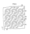
- FIG. 3 shows a top view of a carrier plate T30 into which gas discharge channels G30 are introduced in the grid dimension of the wiring to be tested.
- a sheet of parallel busbar S30, photoconductor P30 and electrodes E30 are applied to the surface of the carrier plate T30 using thin film technology.
- the collecting lines S30 are guided in an arc around the gas discharge channels G30 in one direction, while the photoconductors P30 are guided in an arc around the gas discharge channels G30 in the other direction.
- the electrodes E30 adjoining the photoconductor P30 initially take a short arcuate course and then their ends protrude into the corresponding gas discharge channels G30.
- the manifolds S30 run at an angle of 45 ° across the main directions x and y of the wiring to be tested tung. This has the advantage that those measuring points that are initially assigned to the same bus can also be controlled. In this case, the entire carrier plate T30 is then rotated through an angle of 90 ° or 270 ° relative to the wiring to be tested. After such a twist, two different collecting lines are then assigned to the two measuring points.
- FIG. 4 shows an arrangement largely corresponding to FIG. 2, in which, however, the control of the individual measuring points is further simplified by an additional optical multiplexer.
- Photoconductor P40 a family of partially transparent busbars S40, photoresistors Pw and two partially transparent lines Le crossing all busbars S40 are applied to the carrier plate (not shown here) using thin film technology.
- the photoconductors P40 are designed as thin circular disks, which are located below the collecting lines S40 and are each connected to the electrode of a gas discharge channel which cannot be seen in FIG. 4.
- the photoresistors Pw which correspond to the photoconductors P40, are also formed as thin circular disks and are each arranged at the intersection of the collecting lines S40 and the lines Le between a collecting line S40 and a line Le.
- FIG. 4 also shows a conductor track Lb which connects measuring points M40 and M41 to one another.
- the two assigned photoconductors P40 and the two assigned photoresistors Pw of the optical multiplexer are exposed to light L, which is again carried out with the aid of an acousto-optically deflectable laser beam in view of the recombination time or decay time .
- the two photoconductors P40 exposed to light L and the two photo resistors Pw exposed to light L then become low-resistance, so that twice the ignition voltage is applied to the gas discharge paths via the two lines Le. An ignition of the gas discharge stretch then offers the guarantee that the conductor track Lb is not interrupted.
- FIG. 5 shows an overall perspective view of the device shown schematically in FIG. 4.
- a carrier plate T40 for example 1000 ⁇ 1000 raster points is shown, with each raster point being assigned a photoconductor P40 according to FIG. 4.
- the two lines Le are then assigned 2,000 photoresistors Pw according to FIG. 4.
- a laser La such as e.g. a He laser or Ne laser, the beam of which can be directed as light L onto each of the 106 photoconductors and the 2000 photoresistors.
- the deflection takes place via an acousto-optical deflector A.
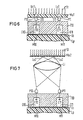
- FIG. 6 shows a first variant of the basic principle shown in FIG. 1.
- the selected photoconductors are exposed to light here via a radiation St distributed over a surface and a mask Ma1 placed on the carrier plate T10.
- the mask Ma1 only transmits the radiation in the area of holes Lo1 which are assigned to the selected gas discharge channels G10 and G11 or the measuring points M10 and M11. It can be seen that the targeted application of selected photoconductors and optionally also selected photoresistors Pw according to FIG. 4 can be controlled via the respective position of holes Lo1 of a mask Ma1 or several masks.
- FIG. 7 shows a second variant of the basic principle shown in FIG. 1.
- the radiation St illuminates a mask Ma2, the holes Lo2 of which are imaged onto the photoconductors P10 and P11 via a lens system Li and thus cause them to be exposed to light.
Landscapes
- Physics & Mathematics (AREA)
- General Physics & Mathematics (AREA)
- Testing Of Short-Circuits, Discontinuities, Leakage, Or Incorrect Line Connections (AREA)
- Manufacture Of Electron Tubes, Discharge Lamp Vessels, Lead-In Wires, And The Like (AREA)
- Tests Of Electronic Circuits (AREA)
Applications Claiming Priority (2)
| Application Number | Priority Date | Filing Date | Title |
|---|---|---|---|
| DE3710595 | 1987-03-31 | ||
| DE3710595 | 1987-03-31 |
Publications (2)
| Publication Number | Publication Date |
|---|---|
| EP0285798A2 true EP0285798A2 (fr) | 1988-10-12 |
| EP0285798A3 EP0285798A3 (fr) | 1990-03-07 |
Family
ID=6324410
Family Applications (1)
| Application Number | Title | Priority Date | Filing Date |
|---|---|---|---|
| EP88103017A Withdrawn EP0285798A3 (fr) | 1987-03-31 | 1988-02-29 | Dispositif de test électrique du fonctionnement de rangées de fils électriques, en particulier pour cartes de circuit |
Country Status (3)
| Country | Link |
|---|---|
| US (1) | US4891578A (fr) |
| EP (1) | EP0285798A3 (fr) |
| JP (1) | JPS63256876A (fr) |
Cited By (2)
| Publication number | Priority date | Publication date | Assignee | Title |
|---|---|---|---|---|
| WO1991002986A1 (fr) * | 1989-08-23 | 1991-03-07 | Siemens Nixdorf Informationssysteme Aktiengesellschaft | Dispositif pour le controle du fonctionnement electrique de champs de cablage, en particulier de cartes de circuits imprimes |
| CN106872878A (zh) * | 2017-02-21 | 2017-06-20 | 济南浪潮高新科技投资发展有限公司 | 一种pcb中自动检测电气连接的方法及系统 |
Families Citing this family (10)
| Publication number | Priority date | Publication date | Assignee | Title |
|---|---|---|---|---|
| US5017863A (en) * | 1989-10-20 | 1991-05-21 | Digital Equipment Corporation | Electro-emissive laser stimulated test |
| US5574382A (en) * | 1991-09-17 | 1996-11-12 | Japan Synthetic Rubber Co., Ltd. | Inspection electrode unit for printed wiring board |
| DE4200404B4 (de) * | 1992-01-10 | 2006-04-06 | Atg Test Systems Gmbh & Co.Kg | Vorrichtung zur elektrischen Prüfung und Verfahren |
| US5202623A (en) * | 1992-02-26 | 1993-04-13 | Digital Equipment Corporation | Laser-activated plasma chamber for non-contact testing |
| JPH07140209A (ja) * | 1993-09-20 | 1995-06-02 | Fujitsu Ltd | 回路配線基板の検査装置およびその検査方法 |
| US5587664A (en) * | 1995-07-12 | 1996-12-24 | Exsight Ltd. | Laser-induced metallic plasma for non-contact inspection |
| JPH0949867A (ja) * | 1995-08-08 | 1997-02-18 | Okano Hightech Kk | 基板検査方法及び装置 |
| US5818239A (en) * | 1997-03-05 | 1998-10-06 | International Business Machines Corporation | Simplified contactless test of MCM thin film I/O nets using a plasma |
| JP3818360B2 (ja) | 2000-10-20 | 2006-09-06 | 信越化学工業株式会社 | 有機ハロシランの製造方法 |
| DE102012022185B4 (de) * | 2012-11-12 | 2015-01-22 | Dräger Medical GmbH | Inkubator mit beschichteter Inkubatorhaube |
Family Cites Families (8)
| Publication number | Priority date | Publication date | Assignee | Title |
|---|---|---|---|---|
| US3737668A (en) * | 1970-07-30 | 1973-06-05 | Marconi Co Ltd | Keyboard |
| JPS4823385A (fr) * | 1971-07-28 | 1973-03-26 | ||
| US3956698A (en) * | 1974-02-12 | 1976-05-11 | Westinghouse Electric Corporation | Contactless test method for integrated circuits |
| DE2508393C2 (de) * | 1975-02-26 | 1983-02-17 | Siemens AG, 1000 Berlin und 8000 München | Gasentladungsanzeigevorrichtung und Verfahren zu ihrem Betrieb |
| DE3116611C2 (de) * | 1980-05-01 | 1985-05-15 | Hitachi, Ltd., Tokio/Tokyo | Vorrichtung zur Messung von Halbleitereigenschaften |
| DE3231598A1 (de) * | 1982-08-25 | 1984-03-01 | Siemens AG, 1000 Berlin und 8000 München | Verfahren und vorrichtung zur elektrischen pruefung von mikroverdrahtungen |
| ATE52620T1 (de) * | 1985-09-04 | 1990-05-15 | Siemens Ag | Vorrichtung fuer die elektrische funktionspruefung von verdrahtungsfeldern, insbesondere von leiterplatten. |
| EP0218058B1 (fr) * | 1985-09-04 | 1990-05-09 | Siemens Aktiengesellschaft | Procédé pour tester le fonctionnement électrique de plage de connexion, en particulier d'un circuit imprimé |
-
1988
- 1988-02-29 EP EP88103017A patent/EP0285798A3/fr not_active Withdrawn
- 1988-03-16 US US07/168,965 patent/US4891578A/en not_active Expired - Fee Related
- 1988-03-29 JP JP63077941A patent/JPS63256876A/ja active Pending
Cited By (3)
| Publication number | Priority date | Publication date | Assignee | Title |
|---|---|---|---|---|
| WO1991002986A1 (fr) * | 1989-08-23 | 1991-03-07 | Siemens Nixdorf Informationssysteme Aktiengesellschaft | Dispositif pour le controle du fonctionnement electrique de champs de cablage, en particulier de cartes de circuits imprimes |
| US5148102A (en) * | 1989-08-23 | 1992-09-15 | Siemens Aktiengesellschaft | Apparatus for the electrical function testing of wiring matrices, particularly of printed circuit boards |
| CN106872878A (zh) * | 2017-02-21 | 2017-06-20 | 济南浪潮高新科技投资发展有限公司 | 一种pcb中自动检测电气连接的方法及系统 |
Also Published As
| Publication number | Publication date |
|---|---|
| US4891578A (en) | 1990-01-02 |
| JPS63256876A (ja) | 1988-10-24 |
| EP0285798A3 (fr) | 1990-03-07 |
Similar Documents
| Publication | Publication Date | Title |
|---|---|---|
| EP0285799B1 (fr) | Dispositif de test électrique du fonctionnement de rangées de fils électriques, en particulier pour cartes de circuit | |
| DE2360801C2 (de) | Schaltungsprüfeinrichtung für integrierte Schaltkreise auf Schichtschaltungsträgern | |
| DE2319011C2 (de) | Verfahren zum Prüfen eines Leiternetzes auf einem isolierenden Substrat und Anordnung zur Durchführung des Verfahrens | |
| DE3408704C2 (de) | Verfahren zum Prüfen von starren oder flexiblen elektrischen Verbindungsnetzwerk-Schaltungen und Vorrichtung zur Durchführung des Verfahrens | |
| DE2744299C2 (de) | Verfahren zum elektrischen Prüfen eines Leiterbahnmusters auf einem Substrat | |
| EP0216135B1 (fr) | Dispositif pour tester le fonctionnement électrique des interconnexions des circuits électriques, en particulier des circuits imprimés | |
| EP0078339A1 (fr) | Dispositif de test pour pistes de circuit imprimé ayant au moins une tête comportant une multitude de contacts flexibles | |
| EP0838688B1 (fr) | Appareil et procédé de test de circuits imprimés | |
| DE3716240A1 (de) | Pruefadapter, insbesondere fuer eine integrierte schaltung | |
| EP0470118A1 (fr) | Dispositif de controle pour controler des elements electriques ou electroniques. | |
| DE19507127A1 (de) | Adaptersystem für Baugruppen-Platinen, zu verwenden in einer Prüfeinrichtung | |
| EP0250620B1 (fr) | Procédé et dispositif pour tester électriquement des circuits imprimés | |
| WO2010081834A1 (fr) | Procédé d'essai de plaquettes à circuit imprimé | |
| EP0218058B1 (fr) | Procédé pour tester le fonctionnement électrique de plage de connexion, en particulier d'un circuit imprimé | |
| DE1463767B2 (de) | Anordnung mit einem spiegelgalvanometer zur ueberwachung von stroemen in hochspannungsleitungen | |
| EP0102565A2 (fr) | Méthode et dispositif pour tester électriquement des micro-câblages | |
| EP0343375A1 (fr) | Procédé de réparation d'interruptions dans un parcours conducteur | |
| EP0322607B1 (fr) | Appareil de commande pour un dispositif pour le test de platines de circuits | |
| DE19718637A1 (de) | Vorrichtung und Verfahren zum Prüfen von Leiterplatten | |
| EP0489052B1 (fr) | Dispositif pour le controle du fonctionnement electrique de champs de cablage, en particulier de cartes de circuits imprimes | |
| EP0286814A2 (fr) | Dispositif de commande | |
| DE19714941A1 (de) | Meßkarte und Ein/Ausgang-Anschlußtestsystem unter Verwendung derselben | |
| DE2655841C3 (de) | Integrierter Widerstandsbaustein zum Einlöten in eine Flachbaugruppe | |
| EP1317674A1 (fr) | Procede et dispositif permettant de tester le fonctionnement de cartes de circuits imprimes | |
| DE4200404B4 (de) | Vorrichtung zur elektrischen Prüfung und Verfahren |
Legal Events
| Date | Code | Title | Description |
|---|---|---|---|
| PUAI | Public reference made under article 153(3) epc to a published international application that has entered the european phase |
Free format text: ORIGINAL CODE: 0009012 |
|
| AK | Designated contracting states |
Kind code of ref document: A2 Designated state(s): AT BE CH DE FR GB IT LI NL |
|
| PUAL | Search report despatched |
Free format text: ORIGINAL CODE: 0009013 |
|
| AK | Designated contracting states |
Kind code of ref document: A3 Designated state(s): AT BE CH DE FR GB IT LI NL |
|
| 17P | Request for examination filed |
Effective date: 19900328 |
|
| 17Q | First examination report despatched |
Effective date: 19920625 |
|
| STAA | Information on the status of an ep patent application or granted ep patent |
Free format text: STATUS: THE APPLICATION IS DEEMED TO BE WITHDRAWN |
|
| 18D | Application deemed to be withdrawn |
Effective date: 19931103 |