EP0216135B1 - Dispositif pour tester le fonctionnement électrique des interconnexions des circuits électriques, en particulier des circuits imprimés - Google Patents
Dispositif pour tester le fonctionnement électrique des interconnexions des circuits électriques, en particulier des circuits imprimés Download PDFInfo
- Publication number
- EP0216135B1 EP0216135B1 EP86111442A EP86111442A EP0216135B1 EP 0216135 B1 EP0216135 B1 EP 0216135B1 EP 86111442 A EP86111442 A EP 86111442A EP 86111442 A EP86111442 A EP 86111442A EP 0216135 B1 EP0216135 B1 EP 0216135B1
- Authority
- EP
- European Patent Office
- Prior art keywords
- gas discharge
- discharge channels
- electrodes
- assigned
- measuring points
- Prior art date
- Legal status (The legal status is an assumption and is not a legal conclusion. Google has not performed a legal analysis and makes no representation as to the accuracy of the status listed.)
- Expired - Lifetime
Links
- 239000011159 matrix material Substances 0.000 claims abstract description 4
- 230000005855 radiation Effects 0.000 claims description 11
- 239000004973 liquid crystal related substance Substances 0.000 claims description 6
- 230000001960 triggered effect Effects 0.000 claims description 2
- 230000000977 initiatory effect Effects 0.000 claims 3
- 230000005865 ionizing radiation Effects 0.000 abstract description 23
- 239000007789 gas Substances 0.000 description 95
- 239000000523 sample Substances 0.000 description 11
- 238000011990 functional testing Methods 0.000 description 9
- 239000004020 conductor Substances 0.000 description 8
- 239000011521 glass Substances 0.000 description 6
- 238000005259 measurement Methods 0.000 description 6
- 238000004519 manufacturing process Methods 0.000 description 5
- IJGRMHOSHXDMSA-UHFFFAOYSA-N Atomic nitrogen Chemical compound N#N IJGRMHOSHXDMSA-UHFFFAOYSA-N 0.000 description 4
- 238000009413 insulation Methods 0.000 description 4
- 238000000034 method Methods 0.000 description 4
- 230000009467 reduction Effects 0.000 description 4
- 230000004913 activation Effects 0.000 description 2
- 210000002858 crystal cell Anatomy 0.000 description 2
- 239000000203 mixture Substances 0.000 description 2
- 229910052757 nitrogen Inorganic materials 0.000 description 2
- 239000011295 pitch Substances 0.000 description 2
- 101100043224 Mus musculus Spag16 gene Proteins 0.000 description 1
- 210000004027 cell Anatomy 0.000 description 1
- 230000008859 change Effects 0.000 description 1
- 230000008878 coupling Effects 0.000 description 1
- 238000010168 coupling process Methods 0.000 description 1
- 238000005859 coupling reaction Methods 0.000 description 1
- 238000002788 crimping Methods 0.000 description 1
- 230000007423 decrease Effects 0.000 description 1
- 230000005684 electric field Effects 0.000 description 1
- 230000005611 electricity Effects 0.000 description 1
- 230000005670 electromagnetic radiation Effects 0.000 description 1
- 238000005516 engineering process Methods 0.000 description 1
- 238000005530 etching Methods 0.000 description 1
- PCHJSUWPFVWCPO-UHFFFAOYSA-N gold Chemical compound [Au] PCHJSUWPFVWCPO-UHFFFAOYSA-N 0.000 description 1
- 239000010931 gold Substances 0.000 description 1
- 229910052737 gold Inorganic materials 0.000 description 1
- 230000001939 inductive effect Effects 0.000 description 1
- 239000011810 insulating material Substances 0.000 description 1
- 230000000873 masking effect Effects 0.000 description 1
- 239000012299 nitrogen atmosphere Substances 0.000 description 1
- 229910000510 noble metal Inorganic materials 0.000 description 1
- 230000005693 optoelectronics Effects 0.000 description 1
- 238000005476 soldering Methods 0.000 description 1
- 125000006850 spacer group Chemical group 0.000 description 1
Images

Classifications
-
- G—PHYSICS
- G01—MEASURING; TESTING
- G01R—MEASURING ELECTRIC VARIABLES; MEASURING MAGNETIC VARIABLES
- G01R1/00—Details of instruments or arrangements of the types included in groups G01R5/00 - G01R13/00 and G01R31/00
- G01R1/02—General constructional details
- G01R1/06—Measuring leads; Measuring probes
- G01R1/067—Measuring probes
- G01R1/07—Non contact-making probes
- G01R1/072—Non contact-making probes containing ionised gas
-
- G—PHYSICS
- G01—MEASURING; TESTING
- G01R—MEASURING ELECTRIC VARIABLES; MEASURING MAGNETIC VARIABLES
- G01R31/00—Arrangements for testing electric properties; Arrangements for locating electric faults; Arrangements for electrical testing characterised by what is being tested not provided for elsewhere
- G01R31/28—Testing of electronic circuits, e.g. by signal tracer
- G01R31/2801—Testing of printed circuits, backplanes, motherboards, hybrid circuits or carriers for multichip packages [MCP]
- G01R31/2805—Bare printed circuit boards
-
- G—PHYSICS
- G01—MEASURING; TESTING
- G01R—MEASURING ELECTRIC VARIABLES; MEASURING MAGNETIC VARIABLES
- G01R31/00—Arrangements for testing electric properties; Arrangements for locating electric faults; Arrangements for electrical testing characterised by what is being tested not provided for elsewhere
- G01R31/50—Testing of electric apparatus, lines, cables or components for short-circuits, continuity, leakage current or incorrect line connections
Definitions
- the invention relates to a device for the electrical functional test of wiring fields, in particular printed circuit boards, according to the preamble of claim 1.
- the contacting of the selected measuring points is usually carried out via resilient test probes.
- the resilient test probes arranged in accordance with the grid dimension of a wiring field to be tested are fastened by means of spring sleeves which are pressed into a carrier plate and into which the test probes are inserted.
- the smallest distance between the measuring points and the current load usually determine the diameter of the resilient test probes, although 0.69 mm is mentioned as the lower limit for the diameter (Elektronik oder & educatechnik, November 1979, pages 472 and 473 ).
- the invention has for its object to drastically reduce the number of leads in a device of the type mentioned.
- Prerequisite a is a property of the wiring field to be checked in each case, while prerequisites b and c are decisive for unambiguous addressing of the respectively selected measuring points of a wiring field.
- the number of supply lines can be considerably reduced, especially since a larger number of gas discharge channels can also be assigned to the electrode collecting lines.
- the technical feasibility of devices for the electrical functional test of printed circuit boards with large printed circuit board formats and small grid dimensions is significantly facilitated and thus also brings about a decisive reduction in manufacturing costs.
- the additional effort for the addressable exposure of the gas discharge channels to radiation introducing gas discharges can be classified as small compared to the advantages mentioned.
- the measuring points are contacted ionically, i.e. the second electrode of the gas discharge gap is formed directly by the measuring points on the circuit board.
- the advantages of addressing measuring points or gas discharge channels according to the invention with a considerable reduction in the wiring effort also result if the measuring points are made ohmic contact by resilient test probes arranged at the lower end of the gas discharge channels. These resilient test probes then form the second electrode of the gas discharge paths, i.e. they are ionically contacted at the end opposite the tip and can be realized with smaller diameters than the conventional test probes connected with wiring.
- the small grid dimensions in the case of ionic contacting with gas discharge channels open to the measuring points cannot be achieved with test probes.
- the electrodes of the gas discharge channels are connected to one another in rows.
- Such a row-wise combination of the electrode connections is in particular matched to a regular grid arrangement of the measuring points, as is usually the case, for example, with printed circuit boards. The result is a clear and particularly simple laying of the electrode collecting lines.
- the electrode collecting lines run transverse to the main directions of the wiring of the wiring fields to be tested. These measures take into account the fact that two selected measuring points must not be assigned the same electrode collecting line. If the electrode collecting lines run, for example, at an angle of 45 ° to the main directions of the wiring, all measuring points can be reliably detected by rotating the entire support plate by an angle of 90 ° or 270 ° relative to the wiring.
- a further simplification in the manufacture of the device results if the electrodes are formed by sections of the electrode collecting lines crossing the gas discharge channels.
- those techniques which have proven themselves in the production of printed circuit boards or layer circuits can then be used in particular for the production of the electrodes and electrode collecting lines.
- the exposure of selected gas discharge channels to radiation introducing gas discharges can be controlled via beams that can be deflected onto the gas discharge channels.
- proven techniques can be used, such as those used for marking parts with deflectable laser beams (Laser 79 Opto-Electronics, Volumes 2 to 6, July 1979, pages 235 to 239).
- the transparent electrodes can preferably be controlled via assigned collecting lines. A further simplification of the connection and the control of the transparent electrodes results if the transparent electrodes are connected to one another in rows via the collecting lines. Run the collecting line then across the electrode manifolds, this results in a particularly simple matrix addressing of the gas discharge channels assigned to the selected measuring points.
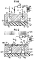
- FIG. 1 shows in a highly simplified schematic representation the principle of operation of a device for the electrical functional test of printed circuit boards on the basis of a contactless ionic contacting of the measuring points via gas discharge paths.
- a part of a circuit board labeled Lp1 can be seen, on the upper side of which the ends of a conductor track Lb1 form measuring points M1 and M2.
- a carrier board Tp1 made of an insulating material such as Glass placed in which a plurality of gas discharge channels is introduced in the form of blind holes.
- the gas discharge channel Gk1 assigned to the measuring point M1 and the gas discharge channel Gk2 assigned to the measuring point M2 are shown.
- An electrode E1 which is connected to an electrode manifold ES1, is arranged on the side of the gas discharge channel Gk1 opposite the measuring point M1.
- an electrode E2 of the gas discharge channel Gk2 is connected to an electrode manifold ES2.
- the electrodes of a multiplicity of gas discharge channels are each connected in rows to one another via the electrode collecting line ES1 and ES2.
- the electrodes E1 and E2 of the associated gas discharge channels Gk1 and Gk2 are activated via the electrode collecting lines ES1 and ES2, this activation being indicated by switches S1 and S2 .
- a series resistor Vw, a voltage source Sq, a current measuring device Sm and an AC voltage generator We are arranged in series between the switches S1 and S2.
- the entire arrangement shown in FIG. 1 is located in an evacuable space under a reduced pressure of, for example, 13.3 10-3 bar (10 torr), the evacuable space being filled with a gas such as e.g. Nitrogen is filled.
- a gas such as e.g. Nitrogen is filled.
- gas discharge paths are formed between the electrode E1 and the measuring point M1 and between the electrode E2 and the measuring point M2, which are connected in series via the conductor track Lb1.
- the voltage of the voltage source Sq is now dimensioned such that twice the operating voltage is applied to these two gas discharge lines connected in series via the switches S1 and S2, the level of which, however, must in no way reach twice the ignition voltage.
- An ignition voltage of the gas discharge paths is only initiated when the gas discharge channels Gk1 and Gk2 assigned to the selected measuring points M1 and M2 are additionally exposed to ionizing radiation iS1 or iS2.
- This ionizing radiation iS1 or iS2 which can be short-wave electromagnetic radiation or corpuscular radiation, reduces the ignition voltage in the gas discharge channels Gk1 and Gk2 to such an extent that the voltage applied via switches S1 and S2 for the ignition the gas discharge path is sufficient.
- an ignition of gas discharges is only possible if the selected gas discharge channels are controlled via their assigned electrode collecting lines and at the same time selectively exposed to radiation, in particular ionizing radiation. In this way, secure addressing of the selected gas discharge channels or measuring points is then also guaranteed.
- the resistance measurements are carried out at the differential reversal point of the gas discharge characteristic, the internal resistances of the gas discharge sections being practically bridged by alternating current. Small fluctuations ⁇ U of the superimposed AC voltage lead to relatively large fluctuations 01 of the current.
- the phase-sensitive current measuring device Sm arranged in the circuit which can be, for example, a commercially available lock-in amplifier, registers the current fluctuations A1 and the resistance R can be determined from the relationship R ⁇ U / ⁇ l. From the level of the determined resistance R, errors can then be deduced, in which the conductor track Lb1 is only partially interrupted. In addition, the determination of the resistance R can also be used for insulation measurements.
- FIG 2 shows a variant in which the carrier plate with Tp10 and the gas discharge channels assigned to the measuring points M1 and M2 are designated Gk10 and Gk11.
- the electrodes E10 and E11 of the gas discharge channels Gk10 and Gk11 are activated in the manner described above via the switches S1 and S2 and corresponding electrode bus lines ES10 and ES11.
- the application of the selected gas discharge channels Gk1 and Gk11 to ionizing radiation iS10 which is initially distributed over a surface, is controlled here with the aid of a mask Mk1 placed on the carrier plate Tp10.
- This mask Mk1 only allows the ionizing radiation iS10 to pass through in areas B1 and B2 which are assigned to the selected gas discharge channels Gk10 and Gk11 or the selected measuring points M1 and M2. It can be seen that the targeted application of selected gas discharge channels can be controlled via the respective position of radiation-permeable areas of a mask or several masks.
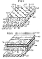
- FIG. 3 shows a perspective view of part of a printed circuit board Lp20, on the surface of which measuring points M20, M21 and M22 arranged in grid dimensions and conductor tracks Lb20, Lb21, Lb22 and Lb23 can be seen.
- the main directions of the conductor tracks, which are perpendicular to one another, are designated HR1 and HR2.
- a support plate Tp20 is placed on the top of the circuit board Lp20, into which a number of cylindrical gas discharge channels Gk20 is inserted.
- the carrier plate Tp20 consists of shaped glass which can be structured photolithographically, into which the gas discharge channels Gk20 are introduced by means of conventional masking and etching techniques.
- electrode collecting lines ES20 run in the surface of the carrier plate Tp20 in which electrode collecting lines ES20 run.
- the electrodes of the gas discharge channels Gk20, designated E20, are formed directly by sections of the electrode collecting lines ES20 crossing the gas discharge channels Gk20.
- the production of the electrode collecting lines ES20 with the associated electrodes E20 can be carried out using techniques customary in the field of printed circuits or layer circuits, with noble metals such as e.g. Gold are suitable.
- the position of the gas discharge channels Gk20 corresponds exactly to the grid of the measuring points of a circuit board Lp20 to be tested, the precise assignment of gas discharge channels Gk20 lying in the sectional plane of the carrier plate Tp20 to the measuring points M20, M21 and M22 located directly underneath being clearly visible. It can also be seen that the number of gas discharge channels Gk20 arranged in rows and columns may well be greater than the number of measuring points present on the circuit board Lp20.
- the electrode collecting lines ES20 run at an angle of 45 ° transversely to the main directions HR1 and HR2 of the conductor tracks of the circuit board Lp20, the reasons for such a choice of direction appearing from the following explanation of the addressing of selected measuring points.
- the gas discharge channels assigned to these measuring points must be exactly detected by appropriate addressing.
- the two gas discharge channels Gk20 marked with an asterisk are electrically controlled via the assigned electrode collecting lines ES20, which is indicated by arrows Pf20 and Pf21.
- the two selected gas discharge channels Gk20, which are marked with an asterisk are additionally and specifically subjected to ionizing radiation iS20 or iS21. It is only with this exposure to the ionizing radiation iS20 and iS21 that the prerequisites for the ignition of gas discharges are created. If the gas discharges actually ignite, it can be concluded from this that there is an electrically conductive connection between the selected measuring points. Conductivity and insulation measurements can be carried out in the manner described in connection with FIG. 1.
- the addressing described above only fails if the same measuring manifold ES20 is assigned to the selected measuring points or gas discharge channels Gk20. Such measuring points can then be detected by additionally using a second carrier plate with a different course of the electrode collecting lines or by using the existing carrier plate Tp20 in a second step in an arrangement rotated by an angle of 90 ° or 270 °.
- FIG. 4 shows a first possibility of how the controllable exposure of the gas discharge channels to ionizing radiation can be realized in the arrangement shown in FIG. 3.
- the selected gas discharge channels Gk20 are acted upon with ionizing radiation denoted here by iS30 and iS31 with the aid of deflectable laser beams, the directions of the deflection being indicated by a flat x, y coordinate system.
- the ionizing radiation iS30 or iS31 in the form of focused laser beams can be deflected from above into the two selected gas discharge channels Gk20 by appropriate deflection of the deflection mirrors As1 and As2.
- the carrier plate Tp20 can also be covered with a cover plate, not shown in FIG. 4, which must be transparent to the ionizing radiation iS30 or iS31 and is made of glass, for example.
- the deflection of the ionizing radiation iS30 or iS31 can be controlled in a simple manner according to the respective test program via computers or microcomputers.
- FIG. 5 shows a second possibility of how in the arrangement shown in FIG. 3 the controllable exposure of the gas discharge channels to ionizing radiation can be realized.
- the selected gas discharge channels Gk20 are acted upon with areal ionizing radiation, referred to here as iS40, for example UV radiation directed in parallel via a parabolic mirror, using a controllable mask Mk2.
- the mask Mk2 placed on the upper side of the carrier plate Tp20 is formed by a liquid crystal cell which is constructed in the manner of a liquid crystal display.
- the thin cell consists of two plane-parallel glass plates Gpo and Gpu, which are spaced apart by spacers Ds and between which there is a liquid crystal mixture Fkm.
- the underside of the upper glass plate Gpo is vapor-coated with a translucent grid, this grid forming transparent electrodes E11 assigned to the gas discharge channels Gk20 and collecting lines Sa connecting these electrodes E11 in rows.
- the underside of the lower glass plate Gpu is vapor-coated over the entire surface with an electrode E12, an outer connecting line A1 being associated with this transparent electrode E2.
- a voltage is applied to a collecting line Sa and the connecting line A1
- the transparency of the liquid crystal mixture Fkm changes in the associated electric field, i.e. it becomes cloudy and becomes opaque to the ionizing radiation iS40 in the area below the transparent electrodes E11 of the horizontal line assigned to the collecting line Sa.
- all the collecting lines Sa can now be controlled in such a way that no ionizing radiation iS40 gets into the gas discharge channels Gk20. If the connection of a collecting line Sa is now switched off in a targeted manner, the assigned horizontal row of gas discharge channels Gk20 is exposed to the ionizing radiation iS40.
- the fact that the collecting line Sa and the electrode collecting lines ES20 run transversely to one another at an angle of 45 ° enables matrix addressing of the selected measuring points or gas discharge channels Gk20. If there are two selected measuring points or gas discharge channels Gk20 in the same horizontal line, only a single collecting line Sa is switched off, while in all other cases two assigned collecting lines Sa are switched off with two measuring points.
- the grid dimension of the measuring points and thus also of the gas discharge channels Gk20 is, for example, 1/40 ", ie approximately 0.6 mm.
- the diameter of the gas discharge channels Gk20 is then 0.3 mm and that of the thickness distance d between the electrodes E20 and the associated measuring points 0.5 mm corresponding to the carrier plate Tp20
- mm (5 torr - mm) with nitrogen the minimum of the normal ignition voltage is around 350 V.
- a voltage of 650 V is then applied to the electrode collecting lines, see above that the ignition of the gas discharges can only be triggered by the reduction of the double ignition voltage by an ionizing radiation.
- the applied voltage between the double burning voltage and the double the normal ignition voltage.
Landscapes
- Physics & Mathematics (AREA)
- General Physics & Mathematics (AREA)
- Engineering & Computer Science (AREA)
- Computer Hardware Design (AREA)
- Microelectronics & Electronic Packaging (AREA)
- General Engineering & Computer Science (AREA)
- Gas-Filled Discharge Tubes (AREA)
- Testing Of Short-Circuits, Discontinuities, Leakage, Or Incorrect Line Connections (AREA)
- Glass Compositions (AREA)
- Measurement Of Radiation (AREA)
- Structure Of Printed Boards (AREA)
Claims (10)
Priority Applications (1)
| Application Number | Priority Date | Filing Date | Title |
|---|---|---|---|
| AT86111442T ATE52620T1 (de) | 1985-09-04 | 1986-08-19 | Vorrichtung fuer die elektrische funktionspruefung von verdrahtungsfeldern, insbesondere von leiterplatten. |
Applications Claiming Priority (2)
| Application Number | Priority Date | Filing Date | Title |
|---|---|---|---|
| DE3531594 | 1985-09-04 | ||
| DE3531594 | 1985-09-04 |
Publications (2)
| Publication Number | Publication Date |
|---|---|
| EP0216135A1 EP0216135A1 (fr) | 1987-04-01 |
| EP0216135B1 true EP0216135B1 (fr) | 1990-05-09 |
Family
ID=6280120
Family Applications (1)
| Application Number | Title | Priority Date | Filing Date |
|---|---|---|---|
| EP86111442A Expired - Lifetime EP0216135B1 (fr) | 1985-09-04 | 1986-08-19 | Dispositif pour tester le fonctionnement électrique des interconnexions des circuits électriques, en particulier des circuits imprimés |
Country Status (5)
| Country | Link |
|---|---|
| US (1) | US4705329A (fr) |
| EP (1) | EP0216135B1 (fr) |
| JP (1) | JPH0625798B2 (fr) |
| AT (1) | ATE52620T1 (fr) |
| DE (1) | DE3671110D1 (fr) |
Families Citing this family (15)
| Publication number | Priority date | Publication date | Assignee | Title |
|---|---|---|---|---|
| ATE92191T1 (de) * | 1987-03-31 | 1993-08-15 | Siemens Ag | Vorrichtung fuer die elektrische funktionspruefung von verdrahtungsfeldern, insbesondere von leiterplatten. |
| EP0285798A3 (fr) * | 1987-03-31 | 1990-03-07 | Siemens Aktiengesellschaft | Dispositif de test électrique du fonctionnement de rangées de fils électriques, en particulier pour cartes de circuit |
| ATE104059T1 (de) * | 1987-12-21 | 1994-04-15 | Siemens Ag | Ansteuereinrichtung fuer die vorrichtung zur elektrischen funktionspruefung von verdrahtungsfeldern. |
| US4970461A (en) * | 1989-06-26 | 1990-11-13 | Lepage Andrew J | Method and apparatus for non-contact opens/shorts testing of electrical circuits |
| DE3927842A1 (de) * | 1989-08-23 | 1991-02-28 | Siemens Ag | Vorrichtung fuer die elektrische funktionspruefung von verdrahtungsfeldern, insbesondere von leiterplatten |
| EP0498007A1 (fr) * | 1991-02-06 | 1992-08-12 | International Business Machines Corporation | Méthode et appareil pour l'essai sans contact |
| US5202623A (en) * | 1992-02-26 | 1993-04-13 | Digital Equipment Corporation | Laser-activated plasma chamber for non-contact testing |
| DE4310573A1 (de) * | 1993-03-31 | 1994-10-06 | Siemens Ag | Plasmaadapter mit Matrixadressierung für die elektrische Funktionsprüfung von Verdrahtungsfeldern, insbesondere von Leiterplatten |
| JPH07140209A (ja) * | 1993-09-20 | 1995-06-02 | Fujitsu Ltd | 回路配線基板の検査装置およびその検査方法 |
| US5587664A (en) * | 1995-07-12 | 1996-12-24 | Exsight Ltd. | Laser-induced metallic plasma for non-contact inspection |
| IL122654A0 (en) * | 1997-12-18 | 1998-08-16 | Exsight Electro Optical System | Method and apparatus for guiding electric current |
| US6118285A (en) * | 1998-01-28 | 2000-09-12 | Probot, Inc | Non-contact plasma probe for testing electrical continuity of printed wire boards |
| AU1503499A (en) * | 1998-04-27 | 1999-11-16 | Exsight Electro Optical Systems Ltd. | Method and apparatus for testing interconnect networks using guided electric currents |
| JP2001221824A (ja) * | 2000-02-10 | 2001-08-17 | Oht Inc | 検査装置及び検査方法、検査ユニット |
| US20060139041A1 (en) * | 2004-12-23 | 2006-06-29 | Nystrom Michael J | System and method of testing and utilizing a fluid stream |
Family Cites Families (3)
| Publication number | Priority date | Publication date | Assignee | Title |
|---|---|---|---|---|
| US4507605A (en) * | 1982-05-17 | 1985-03-26 | Testamatic, Incorporated | Method and apparatus for electrical and optical inspection and testing of unpopulated printed circuit boards and other like items |
| DE3231598A1 (de) * | 1982-08-25 | 1984-03-01 | Siemens AG, 1000 Berlin und 8000 München | Verfahren und vorrichtung zur elektrischen pruefung von mikroverdrahtungen |
| DE3235119A1 (de) * | 1982-09-22 | 1984-03-22 | Siemens AG, 1000 Berlin und 8000 München | Anordnung fuer die pruefung von mikroverdrahtungen und verfahren zu ihrem betrieb |
-
1986
- 1986-08-19 EP EP86111442A patent/EP0216135B1/fr not_active Expired - Lifetime
- 1986-08-19 DE DE8686111442T patent/DE3671110D1/de not_active Expired - Lifetime
- 1986-08-19 AT AT86111442T patent/ATE52620T1/de not_active IP Right Cessation
- 1986-09-01 JP JP61205746A patent/JPH0625798B2/ja not_active Expired - Lifetime
- 1986-09-02 US US06/902,744 patent/US4705329A/en not_active Expired - Fee Related
Also Published As
| Publication number | Publication date |
|---|---|
| ATE52620T1 (de) | 1990-05-15 |
| US4705329A (en) | 1987-11-10 |
| DE3671110D1 (de) | 1990-06-13 |
| JPS6256871A (ja) | 1987-03-12 |
| EP0216135A1 (fr) | 1987-04-01 |
| JPH0625798B2 (ja) | 1994-04-06 |
Similar Documents
| Publication | Publication Date | Title |
|---|---|---|
| EP0285799B1 (fr) | Dispositif de test électrique du fonctionnement de rangées de fils électriques, en particulier pour cartes de circuit | |
| DE2319011C2 (de) | Verfahren zum Prüfen eines Leiternetzes auf einem isolierenden Substrat und Anordnung zur Durchführung des Verfahrens | |
| EP0216135A1 (fr) | Dispositif pour tester le fonctionnement électrique des interconnexions des circuits électriques, en particulier des circuits imprimés | |
| DE2360801A1 (de) | Pruefeinrichtung mit kontaktiereinrichtung | |
| EP0838688B1 (fr) | Appareil et procédé de test de circuits imprimés | |
| EP0523594A1 (fr) | Procédé pour tester des substrats pour dispositifs d'affichage à cristal liquide utilisant un faisceau corpusculaire | |
| EP0470118A1 (fr) | Dispositif de controle pour controler des elements electriques ou electroniques. | |
| DE4231185A1 (de) | Pruefelektrodeneinheit fuer gedruckte schaltungen, pruefgeraet, das die pruefelektrodeneinheit umfasst, und verfahren zum pruefen gedruckter schaltungen, das das pruefgeraet verwendet | |
| EP0218058B1 (fr) | Procédé pour tester le fonctionnement électrique de plage de connexion, en particulier d'un circuit imprimé | |
| DE19507127A1 (de) | Adaptersystem für Baugruppen-Platinen, zu verwenden in einer Prüfeinrichtung | |
| EP0250620B1 (fr) | Procédé et dispositif pour tester électriquement des circuits imprimés | |
| DE10042224C2 (de) | Modultestsockel für Prüfadapter | |
| EP0102565A2 (fr) | Méthode et dispositif pour tester électriquement des micro-câblages | |
| EP0285798A2 (fr) | Dispositif de test électrique du fonctionnement de rangées de fils électriques, en particulier pour cartes de circuit | |
| EP0142119A1 (fr) | Dispositif pour adapter le pas d'une grille de contact d'un appareil de contrôle de circuits imprimés | |
| EP0322607B1 (fr) | Appareil de commande pour un dispositif pour le test de platines de circuits | |
| EP0875767B1 (fr) | Appareil et procédé pour tester des circuits imprimés non pourvus de composants | |
| DE9004562U1 (de) | Prüfvorrichtung zum Prüfen von elektrischen oder elektronischen Prüflingen | |
| EP0489052B1 (fr) | Dispositif pour le controle du fonctionnement electrique de champs de cablage, en particulier de cartes de circuits imprimes | |
| WO2004059329A1 (fr) | Adaptateur permettant de tester des structures a conducteurs | |
| DE3530827C2 (fr) | ||
| EP0286814A2 (fr) | Dispositif de commande | |
| DE68915781T2 (de) | Elektrische testsonde. | |
| DE4200404B4 (de) | Vorrichtung zur elektrischen Prüfung und Verfahren | |
| EP1317674A1 (fr) | Procede et dispositif permettant de tester le fonctionnement de cartes de circuits imprimes |
Legal Events
| Date | Code | Title | Description |
|---|---|---|---|
| PUAI | Public reference made under article 153(3) epc to a published international application that has entered the european phase |
Free format text: ORIGINAL CODE: 0009012 |
|
| AK | Designated contracting states |
Kind code of ref document: A1 Designated state(s): AT BE CH DE FR GB IT LI NL SE |
|
| 17P | Request for examination filed |
Effective date: 19870424 |
|
| 17Q | First examination report despatched |
Effective date: 19890217 |
|
| GRAA | (expected) grant |
Free format text: ORIGINAL CODE: 0009210 |
|
| AK | Designated contracting states |
Kind code of ref document: B1 Designated state(s): AT BE CH DE FR GB IT LI NL SE |
|
| REF | Corresponds to: |
Ref document number: 52620 Country of ref document: AT Date of ref document: 19900515 Kind code of ref document: T |
|
| REF | Corresponds to: |
Ref document number: 3671110 Country of ref document: DE Date of ref document: 19900613 |
|
| ET | Fr: translation filed | ||
| ITF | It: translation for a ep patent filed | ||
| GBT | Gb: translation of ep patent filed (gb section 77(6)(a)/1977) | ||
| PLBE | No opposition filed within time limit |
Free format text: ORIGINAL CODE: 0009261 |
|
| STAA | Information on the status of an ep patent application or granted ep patent |
Free format text: STATUS: NO OPPOSITION FILED WITHIN TIME LIMIT |
|
| 26N | No opposition filed | ||
| PGFP | Annual fee paid to national office [announced via postgrant information from national office to epo] |
Ref country code: AT Payment date: 19910726 Year of fee payment: 6 |
|
| PGFP | Annual fee paid to national office [announced via postgrant information from national office to epo] |
Ref country code: SE Payment date: 19910816 Year of fee payment: 6 |
|
| PGFP | Annual fee paid to national office [announced via postgrant information from national office to epo] |
Ref country code: BE Payment date: 19910828 Year of fee payment: 6 |
|
| ITTA | It: last paid annual fee | ||
| PG25 | Lapsed in a contracting state [announced via postgrant information from national office to epo] |
Ref country code: AT Effective date: 19920819 |
|
| PG25 | Lapsed in a contracting state [announced via postgrant information from national office to epo] |
Ref country code: SE Effective date: 19920820 |
|
| PG25 | Lapsed in a contracting state [announced via postgrant information from national office to epo] |
Ref country code: BE Effective date: 19920831 |
|
| PGFP | Annual fee paid to national office [announced via postgrant information from national office to epo] |
Ref country code: DE Payment date: 19921023 Year of fee payment: 7 |
|
| PGFP | Annual fee paid to national office [announced via postgrant information from national office to epo] |
Ref country code: CH Payment date: 19921120 Year of fee payment: 7 |
|
| BERE | Be: lapsed |
Owner name: SIEMENS A.G. Effective date: 19920831 |
|
| PGFP | Annual fee paid to national office [announced via postgrant information from national office to epo] |
Ref country code: GB Payment date: 19930714 Year of fee payment: 8 |
|
| PGFP | Annual fee paid to national office [announced via postgrant information from national office to epo] |
Ref country code: FR Payment date: 19930819 Year of fee payment: 8 |
|
| PG25 | Lapsed in a contracting state [announced via postgrant information from national office to epo] |
Ref country code: LI Effective date: 19930831 Ref country code: CH Effective date: 19930831 |
|
| PGFP | Annual fee paid to national office [announced via postgrant information from national office to epo] |
Ref country code: NL Payment date: 19930831 Year of fee payment: 8 |
|
| REG | Reference to a national code |
Ref country code: CH Ref legal event code: PL |
|
| PG25 | Lapsed in a contracting state [announced via postgrant information from national office to epo] |
Ref country code: DE Effective date: 19940503 |
|
| PG25 | Lapsed in a contracting state [announced via postgrant information from national office to epo] |
Ref country code: GB Effective date: 19940819 |
|
| EUG | Se: european patent has lapsed |
Ref document number: 86111442.9 Effective date: 19930307 |
|
| PG25 | Lapsed in a contracting state [announced via postgrant information from national office to epo] |
Ref country code: NL Effective date: 19950301 |
|
| NLV4 | Nl: lapsed or anulled due to non-payment of the annual fee | ||
| GBPC | Gb: european patent ceased through non-payment of renewal fee |
Effective date: 19940819 |
|
| PG25 | Lapsed in a contracting state [announced via postgrant information from national office to epo] |
Ref country code: FR Effective date: 19950428 |
|
| REG | Reference to a national code |
Ref country code: FR Ref legal event code: ST |
|
| PG25 | Lapsed in a contracting state [announced via postgrant information from national office to epo] |
Ref country code: IT Free format text: LAPSE BECAUSE OF NON-PAYMENT OF DUE FEES;WARNING: LAPSES OF ITALIAN PATENTS WITH EFFECTIVE DATE BEFORE 2007 MAY HAVE OCCURRED AT ANY TIME BEFORE 2007. THE CORRECT EFFECTIVE DATE MAY BE DIFFERENT FROM THE ONE RECORDED. Effective date: 20050819 |