EP0344702A2 - Appareil à circuit électronique - Google Patents
Appareil à circuit électronique Download PDFInfo
- Publication number
- EP0344702A2 EP0344702A2 EP89109709A EP89109709A EP0344702A2 EP 0344702 A2 EP0344702 A2 EP 0344702A2 EP 89109709 A EP89109709 A EP 89109709A EP 89109709 A EP89109709 A EP 89109709A EP 0344702 A2 EP0344702 A2 EP 0344702A2
- Authority
- EP
- European Patent Office
- Prior art keywords
- electric circuit
- portions
- conjunction
- electrically connecting
- connecting member
- Prior art date
- Legal status (The legal status is an assumption and is not a legal conclusion. Google has not performed a legal analysis and makes no representation as to the accuracy of the status listed.)
- Granted
Links
Images


Classifications
-
- H—ELECTRICITY
- H10—SEMICONDUCTOR DEVICES; ELECTRIC SOLID-STATE DEVICES NOT OTHERWISE PROVIDED FOR
- H10W—GENERIC PACKAGES, INTERCONNECTIONS, CONNECTORS OR OTHER CONSTRUCTIONAL DETAILS OF DEVICES COVERED BY CLASS H10
- H10W74/00—Encapsulations, e.g. protective coatings
- H10W74/01—Manufacture or treatment
- H10W74/019—Manufacture or treatment using temporary auxiliary substrates
-
- H—ELECTRICITY
- H10—SEMICONDUCTOR DEVICES; ELECTRIC SOLID-STATE DEVICES NOT OTHERWISE PROVIDED FOR
- H10P—GENERIC PROCESSES OR APPARATUS FOR THE MANUFACTURE OR TREATMENT OF DEVICES COVERED BY CLASS H10
- H10P72/00—Handling or holding of wafers, substrates or devices during manufacture or treatment thereof
- H10P72/70—Handling or holding of wafers, substrates or devices during manufacture or treatment thereof for supporting or gripping
- H10P72/74—Handling or holding of wafers, substrates or devices during manufacture or treatment thereof for supporting or gripping using temporarily an auxiliary support
-
- H—ELECTRICITY
- H10—SEMICONDUCTOR DEVICES; ELECTRIC SOLID-STATE DEVICES NOT OTHERWISE PROVIDED FOR
- H10W—GENERIC PACKAGES, INTERCONNECTIONS, CONNECTORS OR OTHER CONSTRUCTIONAL DETAILS OF DEVICES COVERED BY CLASS H10
- H10W70/00—Package substrates; Interposers; Redistribution layers [RDL]
- H10W70/60—Insulating or insulated package substrates; Interposers; Redistribution layers
- H10W70/62—Insulating or insulated package substrates; Interposers; Redistribution layers characterised by their interconnections
- H10W70/63—Vias, e.g. via plugs
- H10W70/635—Through-vias
-
- H—ELECTRICITY
- H10—SEMICONDUCTOR DEVICES; ELECTRIC SOLID-STATE DEVICES NOT OTHERWISE PROVIDED FOR
- H10W—GENERIC PACKAGES, INTERCONNECTIONS, CONNECTORS OR OTHER CONSTRUCTIONAL DETAILS OF DEVICES COVERED BY CLASS H10
- H10W72/00—Interconnections or connectors in packages
- H10W72/01—Manufacture or treatment
- H10W72/0198—Manufacture or treatment batch processes
-
- H—ELECTRICITY
- H10—SEMICONDUCTOR DEVICES; ELECTRIC SOLID-STATE DEVICES NOT OTHERWISE PROVIDED FOR
- H10W—GENERIC PACKAGES, INTERCONNECTIONS, CONNECTORS OR OTHER CONSTRUCTIONAL DETAILS OF DEVICES COVERED BY CLASS H10
- H10W76/00—Containers; Fillings or auxiliary members therefor; Seals
- H10W76/60—Seals
-
- H—ELECTRICITY
- H10—SEMICONDUCTOR DEVICES; ELECTRIC SOLID-STATE DEVICES NOT OTHERWISE PROVIDED FOR
- H10W—GENERIC PACKAGES, INTERCONNECTIONS, CONNECTORS OR OTHER CONSTRUCTIONAL DETAILS OF DEVICES COVERED BY CLASS H10
- H10W90/00—Package configurations
-
- H—ELECTRICITY
- H10—SEMICONDUCTOR DEVICES; ELECTRIC SOLID-STATE DEVICES NOT OTHERWISE PROVIDED FOR
- H10P—GENERIC PROCESSES OR APPARATUS FOR THE MANUFACTURE OR TREATMENT OF DEVICES COVERED BY CLASS H10
- H10P72/00—Handling or holding of wafers, substrates or devices during manufacture or treatment thereof
- H10P72/70—Handling or holding of wafers, substrates or devices during manufacture or treatment thereof for supporting or gripping
- H10P72/74—Handling or holding of wafers, substrates or devices during manufacture or treatment thereof for supporting or gripping using temporarily an auxiliary support
- H10P72/743—Handling or holding of wafers, substrates or devices during manufacture or treatment thereof for supporting or gripping using temporarily an auxiliary support used as a support during manufacture of interconnect decals or build up layers
-
- H—ELECTRICITY
- H10—SEMICONDUCTOR DEVICES; ELECTRIC SOLID-STATE DEVICES NOT OTHERWISE PROVIDED FOR
- H10W—GENERIC PACKAGES, INTERCONNECTIONS, CONNECTORS OR OTHER CONSTRUCTIONAL DETAILS OF DEVICES COVERED BY CLASS H10
- H10W72/00—Interconnections or connectors in packages
- H10W72/071—Connecting or disconnecting
- H10W72/072—Connecting or disconnecting of bump connectors
- H10W72/07251—Connecting or disconnecting of bump connectors characterised by changes in properties of the bump connectors during connecting
-
- H—ELECTRICITY
- H10—SEMICONDUCTOR DEVICES; ELECTRIC SOLID-STATE DEVICES NOT OTHERWISE PROVIDED FOR
- H10W—GENERIC PACKAGES, INTERCONNECTIONS, CONNECTORS OR OTHER CONSTRUCTIONAL DETAILS OF DEVICES COVERED BY CLASS H10
- H10W72/00—Interconnections or connectors in packages
- H10W72/20—Bump connectors, e.g. solder bumps or copper pillars; Dummy bumps; Thermal bumps
-
- H—ELECTRICITY
- H10—SEMICONDUCTOR DEVICES; ELECTRIC SOLID-STATE DEVICES NOT OTHERWISE PROVIDED FOR
- H10W—GENERIC PACKAGES, INTERCONNECTIONS, CONNECTORS OR OTHER CONSTRUCTIONAL DETAILS OF DEVICES COVERED BY CLASS H10
- H10W72/00—Interconnections or connectors in packages
- H10W72/50—Bond wires
- H10W72/531—Shapes of wire connectors
- H10W72/536—Shapes of wire connectors the connected ends being ball-shaped
-
- H—ELECTRICITY
- H10—SEMICONDUCTOR DEVICES; ELECTRIC SOLID-STATE DEVICES NOT OTHERWISE PROVIDED FOR
- H10W—GENERIC PACKAGES, INTERCONNECTIONS, CONNECTORS OR OTHER CONSTRUCTIONAL DETAILS OF DEVICES COVERED BY CLASS H10
- H10W72/00—Interconnections or connectors in packages
- H10W72/50—Bond wires
- H10W72/531—Shapes of wire connectors
- H10W72/5363—Shapes of wire connectors the connected ends being wedge-shaped
-
- H—ELECTRICITY
- H10—SEMICONDUCTOR DEVICES; ELECTRIC SOLID-STATE DEVICES NOT OTHERWISE PROVIDED FOR
- H10W—GENERIC PACKAGES, INTERCONNECTIONS, CONNECTORS OR OTHER CONSTRUCTIONAL DETAILS OF DEVICES COVERED BY CLASS H10
- H10W72/00—Interconnections or connectors in packages
- H10W72/50—Bond wires
- H10W72/551—Materials of bond wires
- H10W72/552—Materials of bond wires comprising metals or metalloids, e.g. silver
- H10W72/5522—Materials of bond wires comprising metals or metalloids, e.g. silver comprising gold [Au]
-
- H—ELECTRICITY
- H10—SEMICONDUCTOR DEVICES; ELECTRIC SOLID-STATE DEVICES NOT OTHERWISE PROVIDED FOR
- H10W—GENERIC PACKAGES, INTERCONNECTIONS, CONNECTORS OR OTHER CONSTRUCTIONAL DETAILS OF DEVICES COVERED BY CLASS H10
- H10W72/00—Interconnections or connectors in packages
- H10W72/851—Dispositions of multiple connectors or interconnections
- H10W72/874—On different surfaces
- H10W72/877—Bump connectors and die-attach connectors
-
- H—ELECTRICITY
- H10—SEMICONDUCTOR DEVICES; ELECTRIC SOLID-STATE DEVICES NOT OTHERWISE PROVIDED FOR
- H10W—GENERIC PACKAGES, INTERCONNECTIONS, CONNECTORS OR OTHER CONSTRUCTIONAL DETAILS OF DEVICES COVERED BY CLASS H10
- H10W76/00—Containers; Fillings or auxiliary members therefor; Seals
- H10W76/60—Seals
- H10W76/63—Seals characterised by their shape or disposition, e.g. between cap and walls of a container
-
- H—ELECTRICITY
- H10—SEMICONDUCTOR DEVICES; ELECTRIC SOLID-STATE DEVICES NOT OTHERWISE PROVIDED FOR
- H10W—GENERIC PACKAGES, INTERCONNECTIONS, CONNECTORS OR OTHER CONSTRUCTIONAL DETAILS OF DEVICES COVERED BY CLASS H10
- H10W90/00—Package configurations
- H10W90/701—Package configurations characterised by the relative positions of pads or connectors relative to package parts
- H10W90/751—Package configurations characterised by the relative positions of pads or connectors relative to package parts of bond wires
- H10W90/754—Package configurations characterised by the relative positions of pads or connectors relative to package parts of bond wires between a chip and a stacked insulating package substrate, interposer or RDL
Definitions
- the present invention relates to an electric circuit apparatus formed by electrically connecting electric circuit components with an electrically connecting member.
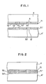
- first semiconductor device 4 and the second semiconductor device 4′ are, as shown in Fig. 2, positioned and welded so that the conjunction portions 5 of the first semiconductor device 4 and the conjunction portions 5′ of the second semiconductor device 4′ are connected to each other with the metal members 70 and 70′.
- the method according to (5) and shown in Fig. 3 is characterized in that: an anisotropic conductive film 78 is interposed between a first circuit substrate 75 and a second circuit substrate 75′, this anisotropic conductive film 78 being formed by having conductive particles 79 dispersed in an insulating material 77.
- the first and second circuit substrates 75 and 75′ are then positioned before application of a pressure alone or a combination of a heat and pressure whereby a junction portion 76 of the first circuit substrate 75 and a junction portion 76′ of a second circuit substrate 75′ are connected to each other.
- the method according to (6) and shown in Fig. 4 is characterized in that: an elastic connector 83 designed such that metal wires 82 made of an insulating material 81 formed by arranging metal wires 82 made of Fe or Cu in the same directions is interposed between the first circuit substrate 75 and the second circuit substrate 75′.
- the first circuit substrate 75 and the second circuit substrate 75′ are then positioned before being pressurized whereby the conjunction portion 76 of the first circuit substrate 75 and the conjunction portion 76′ of the second circuit substrate 75′ are connected to each other.
- a circuit design on the basis of the bonding method involves a certain limitation.
- the pitch (the distance between the central portions of the neighboring junctions) between the neighboring conductors is too large, and the overall thickness of the circuit cannot be reduced.
- the reliability is insufficient because of corrosion and breakage of the conductor, and the characteristics can deteriorate due to the concentration of heat in the portions between the bonding members and the electric circuit members.
- an electric circuit part becomes defective, it cannot be solely replaced.
- an object of the present invention is to provide an electric circuit device capable of overcoming all of the above-described problems and exhibiting high density and satisfactory reliability simply with a reduced cost.
- the same can replace the conventional connecting method and sealing method and in addition it can realize a dense multicontact connection with which the thermal characteristics or the like can be improved.
- An electric circuit apparatus characterized in that the same comprising: an electrically connecting member including a holding body made of an electrically insulating material and a plurality of electrically conductive members embedded in the holding body, wherein end portions of the electrically conductive members appear outside on one side of the holding body while the other end portions of the electrically conductive members appear outside on the other side of the holding body; a plurality of electric circuit components a to which the one end portions of the electrically conductive members are connected; a holding member which holds plurality of the electric circuit components a ; and another electric circuit component b to which the other end portions of the electrically conductive members are connected.
- the electric circuit components according to the present invention are exemplified by: semiconductor elements such as transistors and ICs, circuit substrates such as resin circuit substrates, ceramic substrates, metal substrate, silicon substrates (sometimes abbreviated to "circuit substrate” hereinafter), and lead frames.
- semiconductor elements such as transistors and ICs
- circuit substrates such as resin circuit substrates, ceramic substrates, metal substrate, silicon substrates (sometimes abbreviated to "circuit substrate” hereinafter), and lead frames.
- the electric circuit components to be held by or connected to the electric circuit components holding member may be arranged to be present solely on a surface of the electric circuit holding member or a plurality of the same may be present on a surface.
- the size, shape, and type of th electric circuit components to be held or connected by the electric circuit component holding member may be optionally determined. However, the more the number and the types of the electric circuit components to be held or supported by the electric circuit component holding member increases, the greater the effect obtainable from the present invention becomes considerable.
- the electric circuit components to be connected to the electrically connecting components holding may be arranged to be present solely on a surface of the holding member or a plurality of the same may be present on a surface.
- Electric circuit components having connecting portions are the subject of the present invention.
- the number of the connecting portions may be optionally determined, the more the number of them increases, the greater the effect obtainable from the present invention becomes considerable.
- the connecting portions are made of electrically conductive material.
- the electric circuit component holding member may be made of any material selected from metal, alloy, organic and inorganic materials. Alternately, a material obtained by composing of the above-described materials may be employed.
- the shape and size of the electric circuit holding member may be optionally determined if a connection between the electric circuit components to be held or connected and the corresponding electric circuit components can be equally and stably established. Although the size, the number, and the types of the electric circuit components to be held by or connected to the electric circuit component holding member may be optionally determined, the more the number and the types of them increases, the greater the effect obtainable from the present invention becomes considerable.
- metal or alloy such as Ag, Cu, Al, Be, Ca, Mg, Mo, Fe. Ni, Co, Mn, W, Ti, Pt, Cr, Pd, Nb, Ta, V, and Y.
- the inorganic material is exemplified by: Si, Ge, GaAs, InGaAsp, InP, and a-Si semiconductors; B2O3, Al2O3, Na2O, K2O, CaO, ZnO, BaO, PbO, Sb2O3, As2O3, La2O, ZrO2, BaO, P2O5, TiO2, MgO, SiC, BeO, BP, BN, h-BN, c-BN, AlN, B4C, TaC, TiB2, CrB2, TiN, Si3N4, Ta2O5, and SiO2 ceramics, Ia, Ib, IIa, and IIb diamonds, glass, synthetic quartz, carbon, boron, and the other inorganic materials.
- the organic material may employ, for example, insulating resin that is exemplified by thermosetting resin, ultraviolet curing resin, and thermoplastic resin, exemplified by: polyimide resin, polyphenylene sulfide resin, polyether sulfon resin, polyether imide resin, polysulfon resin, fluororesin, polycarbonate resin, polydiphenylether resin, polybenzil imidazole resin, polyamideimide resin, polypropylene resin, polyvinyl chloride resin, polystylene resin, methacrylate metyl resin, polyphenylene oxide resin, phenol resin, melanin resin, epoxy resin, urea resin, methacrylic resin, vinylidene chloride resin, alkid resin, silicon resin, and so on.
- insulating resin that is exemplified by thermosetting resin, ultraviolet curing resin, and thermoplastic resin, exemplified by: polyimide resin, polyphenylene sulfide resin, polyether sulfon resin, polyether
- a circuit may be formed in the electric circuit component holding member according to the present invention.
- the electric circuit component holding member is made of an insulating material or a material whose surface has been subjected to the insulating treatment
- a circuit pattern and a conjunction portion may be formed on at least a side of the electric circuit component holding member.
- the circuits may be connected to each other on the two sides of the holding member, or holding bodies on which a circuit pattern has been respectively drawn may be layered to form a multilayered substrate.
- a layered structure may be employed that can be obtained by combining materials each of which exhibits individual functions.
- a combination of a circuit substrate and a reinforcing plate or a combination of a circuit substrate and radiating fins may be employed.
- the number of the layers and the functions may be selected optionally.
- the electrically connecting member according to the present invention is formed such that a plurality of conductive members are embedded in a holding body made of an electrically insulating material.
- the conductive members are electrically insulated from each other.
- this conductive member appears on one side of the holding member, while another end of the same appears on the other side of the holding member.
- the electrically connecting members may be formed by a single layer or a multilayer consisting of two or more layers.
- the metal component prefferably be made of gold.
- the following metal or an alloy may be optionally employed, which is exemplified by: metal or an alloy such as Ag, Be, Ca, Mg, Mo, Ni, W, Fe, Ti, In, Ta, Zn, Cu, Al, Sn, and Pb-Sn.
- the metal member and the alloy member may be arranged such that one electrically connecting member may include the same metals or may include individual type metals.
- Each of the metal members and the alloy members of the electrically connecting member may be made of the same metals or alloys, and alternately the same may be made of individual metals or alloys.
- a material prepared by an organic material and/or inorganic material contained in a metal material may be employed if it displays conductivity.
- a material obtained by combining an inorganic material and an organic material may be employed if it displays conductivity.
- the cross-sectional shape of the electrically conductive member may be formed in a circular, rectangular, or other optional shapes.
- the thickness of the electrically conductive member is not specifically limited, but it is preferable for the same to be 20 ⁇ m ⁇ or more, and it can be 20 ⁇ m ⁇ or less.
- the portion of the electrically conductive member that appears outside may be arranged to be the same level as that of the holding body, or it may be arranged to project over the surface of the holding body.
- This projection portion may be formed on one side or on two sides. When the projection arranged to further project, it may be formed in a bump-like shape.
- the interval between the electrically conductive members may be arranged to be the same interval between the conjunction portions of the electric circuit parts, or the same may be arranged to be an interval which is shorter than the former.
- the electric circuit components and the electrically connecting members can be connected to each other without any necessity of performing any positioning of the electric circuit components and the electrically connecting components.
- the electrically conductive member does not need for the electrically conductive member to be arranged to be perpendicular to the holding body, but it may be diagonally arranged from one side of the holding member to another side of the same.
- the holding body is made of an electrically insulating material.
- the electrically insulating material may be exemplified by an organic material and an inorganic material. Alternately, a metal or an alloy which has been subjected to a treatment in which the electrically conductive members are electrically insulated from each other may be employed. One type or a plurality of types of inorganic, metal or alloy in the form of desired shapes such as pulverulent and fiber may be dispersed and contained in the inorganic materials. In the case where the holding member is made of a metal, it needs, for example, for an electrically insulating material such as resin to be disposed between the electrically conductive material and the holding body.
- an electrically insulating material such as resin
- insulating resin such as thermosetting resin, ultraviolet curing resin and thermoplastic resin may be employed as the organic material, the insulating resin being exemplified by: polyimide resin, polyphenylene sulfide resin, polyether sulfon resin, polyether imide resin, polysulfon resin, fluororesin, polycarbonate resin, polydiphenylether resin, polybenzil imidazole resin, polyamideimide resin, polypropylene resin, polyvinyl chloride resin, polystylene resin, methacrylate metyl resin, polyphenylene oxide resin, phenol resin, melanin resin, epoxy resin, urea resin, methacrylic resin, vinylidene chloride resin, alkid resin, silicon resin, and so on.
- polyimide resin polyphenylene sulfide resin
- polyether sulfon resin polyether imide resin
- polysulfon resin fluororesin
- polycarbonate resin polydiphenylether resin
- the inorganic material and the metal material to be employed is exemplified by: SiO2, B2O3, Al2O3, Na2O, K2O, CaO, ZnO, BaO, PbO, Sb2O3, As2O3, La2O3, ZrO2, BaO, P2O5, TiO2, MgO, SiC, BeO, BP, BN, AlN, B4C, TaC, TiB2, CrB2, TiN, Si3N4, Ta2O5 ceramics, and metal or an alloy such as Ag, Cu, Au, Al, Be, Ca, Mg, Mo, Fe, Ni, Si, Co, Mn, and W.
- the end portion of the electrically connecting member can be connected to the electric circuit component by the following three methods wherein one or more electric circuit components may be connected to one electrically connecting member and at least one of the thus-connected electric circuit component needs to be connected in either of the following methods structured such that:
- the conjunction layer to be formed due to metallization becomes a crystalline structure of the same type that forms the electrically conductive member or the conjunction portion.
- a method may, for example, be employed which is arranged such that the end portions of the electrically conductive member and the corresponding conjunction portion which have been brought into contact into each other are heated up to a proper temperature. As a result of this heat, atoms can diffuse in the vicinity of the contact portion, causing the diffused portion to be brought to a metallized state and the conjunction layer is formed.
- the thus-formed conjunction layer are made of an alloy of the above-described metals.
- a method may, for example, be employed which is arranged such that the end portion of the electrically conductive member and the corresponding conjunction portion which have been brought into contact into each other are heated up to a proper temperature. As a result of this heat, atoms can diffuse in the vicinity of the contact portion, causing a layer made of a solid solution or a metallic compound to be formed in the vicinity of the contact portion, this layer being able to serve as the conjunction layer.
- the heating temperature is arranged to 200 to 350 °C.
- the conjunction layer is made of the alloy.
- the above-described metallization or alloying is performed, and the conjunction portion is treated similarly: a case where the plurality of electrically conductive members of a electrically connecting member are made of the same metal or alloy, a case where the same are respectively made of individually metals or alloys, a case where one electrically conductive member is made of the same metal or alloy, a case where one electrically conductive member is made of individual metal or alloy, and the other case.
- the electrically conductive member or the conjunction portion needs to be made of metal or alloy in the contact portion therebetween, and the other portions may be made of a material in which glass is mixed with metal or resin is mixed with metal.
- a plating layer made of metal or alloy that can be readily brought to an alloy may be formed on the surfaces to be connected to each other.
- connection is performed alternately to the above-described connection by metallizing or alloying, a method may be employed, for example, the electric circuit component and the electrically conductive member of the electrically connecting member may be pressed to be connected to each other.
- the following methods (1) to (5) may be employed to hold at least one side other than the sides on which at least one electrically connecting portion is present of the electric circuit component holding member and the electric circuit component and to hold the electrically connecting member and the electric circuit component or the other electric circuit component, where at least one portion of the above needs to be held by at least one of the following methods:
- mechanical portions or functionating portions which serve as references for positioning the electric circuit component holding member and the other electric circuit component and which are disposed in these electric circuit component holding member and the other electric circuit component
- positioning holes, positioning pins, surfaces serving as references, and positioning marks can be employed.
- the shape and the size them may be determined optionally if the mechanical portions or the functionating portions can serves as references for holding or connecting the electric circuit component to the electric circuit component holding member and if the same can serve as reference for positioning the electric circuit component holding member holding or connecting the electric circuit component and the other electric circuit components, that is, the junction portions of the electric circuit component held by or connected to the electric circuit component holding member and the conjunction portion of the other electric circuit component.
- mechanical portions or functionating portions which serve as positioning references to be provided for the electric circuit component holding member, the other electric circuit components and electrically conductive member may be disposed in the central portion or the peripheral portion.
- the longer the interval between the reference portions the positional accuracy can be improved.
- the number of the same is not limited.
- the electric circuit component is arranged to be attached to or detached from the electrically connecting member, the electric circuit components can be replaced at the time of a failure, causing an electric circuit apparatus which can be extremely readily maintained to be obtained.
- the electric circuit component to be held by or connected to the electric circuit component holding member can be readily connected to the other electric circuit component, and a sole electric circuit apparatus can be given a variety of functions whenever the electric circuit component holding member which holds the electric circuit component or which is connected to the electric circuit component is replaced.
- the conjunction portion of the electric circuit component can be disposed in the periphery portion and as well in the portion other than this periphery portion.
- the number of the conjunction portions can be increased, causing a dense structure to be achieved.
- the quantity of the metal material to be used for the electrically connecting member can be reduced, the overall cost can be reduced even if expensive gold is used as the metallic portion.
- the electric circuit component and the other electric circuit component are connected to each other by the electrically connecting member after the electric circuit component has been held by or connected to the electric circuit component holding member, a plurality of and a variety of electric circuit components can be used.
- the connection of the thus-employed electric circuit components is achieved collectively, a variety of electric circuit apparatuses can be manufactured in one manufacturing process.
- the electric circuit components By classifying the electric circuit components to be held by the holding member on the basis of their functions, the electric circuit components can be arranged on the basis of the function groups of the holding members holding or connecting the electric circuit components. Therefore, a further various electric circuit apparatuses can be manufactured from the same manufacturing process.
- the electric circuit components are held by the electric circuit holding member, the electric circuit components do not need to be held by jigs and/or tools during and after completion of the manufacturing the electric circuit apparatus. As a result, control of manufacturing of the electric circuit apparatuses and the same after the manufacturing can be readily performed.
- the electric circuit component and the other electric circuit component are connected to each other with the electrically connecting member after the electric circuit component has been held by the electric circuit component holding member, it does not need to perform complicated positionings of a surface down mount for each of the electric circuit components, and positioning of the conjunction portions of a multiplicity of electric circuit components can be performed. As a result, manufacturing yield can be significantly improved.
- the electric circuit component and the other electric circuit component are collectively positioned and connected to each other with the electrically connecting member after the electric circuit component has been held by the electric circuit component holding member, a variety of electric circuit components can be employed, and the connection of the thus-employed electric circuit components can be simultaneously performed. As a result, a variety of electric circuit apparatuses can be manufactured from the same manufacturing process.
- the electric circuit components can, similarly be, connected to a multiplicity of sides of the electric circuit component and the electrically connecting member.
- 3-D dense electric circuit apparatus can be obtained.
- the insulating body of the electrically conductive member is made of a material with a thermal expansion coefficient approximated to that of the electric circuit component, or when the electric circuit component holding member is made of a material with a thermal expansion coefficient approximated to that of the electric circuit component, any generation of thermal stress and strain can be prevented.
- defects which deteriorate the reliability of the electric circuit apparatus such as cracking of the electric circuit components or change in the characteristics of the electric circuit components due to the application of heat can be prevented.
- a reliable electric circuit apparatus can be obtained.
- the resistance at the conjunction portion between the electric circuit components can be further reduced with respect to the case where only one electric circuit component is connected by metallizing and/or alloying.
- connection of the electric circuit components are achieved by a method other than metallizing and/or alloying, deterioration due to heat from the electric circuit components caused from metallizing and/or alloying can be prevented.
- the electric circuit components are, at needs, intended to be arranged to be a detachable type, a connection of the electric circuit components according to a method other than the metallizing and/or alloying will meet this desire.
- the mechanical portions or functionating portions provided for the electric circuit component holding member, the other electric circuit components, and the electrically connecting members and capable of serving as references for the positional relationship can be accurately achieved. That is, the conjunction portion between the electric circuit components held or connected by the electric circuit component holding member and the conjunction portion of the other electric circuit components can be further accurately positioned. As a result, a further precise connection can be widely equally and stably achieved.
- the connection can be performed at a high speed.
- connection can be simply performed without any positioning.
- the connection is established after the positioning has been achieved accurately, the strength distribution of the connected portions can be significantly uniformed. As a result, reliability can be improved.
- the electric circuit component holding member serves as a cap for sealing the electric circuit component
- heat generated from the electric circuit component can be further quickly discharged outside. Therefore, an electric circuit apparatus exhibiting an excellent heat discharge performance can be obtained.
- water invasion into the apparatus can be protected. Consequently, the circuit portion of the conjunction portions and the electric circuit components can be protected from any corrosion, causing its reliability to be improved.
- any generation of thermal stress or strain due to the difference in the thermal expansion coefficient can be prevented even if the size of the apparatus is enlarged.
- defects which deteriorate the reliability of the electric circuit apparatus such as cracking of the electric circuit components or change in the characteristics of the electric circuit components due to the application of heat can be prevented.
- a reliable electric circuit apparatus can be obtained.
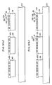
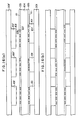
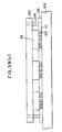
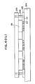
- FIG. 5A and 5B A first embodiment of the present invention will be described with reference to Figs. 5A and 5B and Figs. 6A to 6C.
- Fig. 5A which is a cross-sectional view, a state is illustrated where any connection is not established between: an electric circuit component holding member 201 holding a plurality of semiconductor devices 101 which serves as the electric circuit components; an electrically connecting member 125; and a circuit substrate 104 which serves as the other electric circuit component.
- the number of the semiconductor devices 101 needs to be one or more.
- the electrically connecting member 125 is so arranged that metal components 107 which serve as electrically conductive members are embedded in a holding body 111 which is made of an organic material. An end of the metal member 107 appears on one side of he holding body 111, while another end of this metal member 107 appears on another side of the holding body.
- the electric circuit component holding member 201 comprises a glass substrate which holds, by adhesion, the sides of the semiconductor devices 101 on which no conjunction portions 102 are present, the conjunction portions 102 being disposed by one or more on the other side.
- the semiconductor device 101 includes conjunction portions 102, the conjunction portions 102 being connected, by alloying, to the end portions of the metal members 107 which appear outside on the one side of the holding body 111.
- the circuit substrate 104 includes conjunction portions 105, these conjunction portions 105 being connected to the other end portions of the metal members 107 which appear outside on the other side of the holding body 111.
- Fig. 5B is a cross-sectional view which illustrates a state where the above-described components are integrated as this connection.
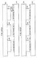
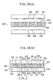
- the electrically connecting member 125 will be described with an example of manufacturing the same described.
- Figs. 6A to 6C are views which illustrate a manufacturing example.
- a 20 ⁇ m ⁇ metal wire 121 made of metal such as gold or the like or an alloy is wound to a rod 122 at a pitch of 40 ⁇ m.
- the thus-wound metal wire 121 is embedded in resin 123 such as polyimide or the like.
- This resin 123 is then hardened after the metal wire 121 has been embedded.
- the hardened resin 123 becomes an insulating body.
- this insulating body in which the metal wire 121 has been embedded therein is cut into slices so that the electrically connecting member 125 is manufactured.
- the thus-manufactured electrically connecting member 125 is shown in Figs. 6B and 6C.
- the metal wire 121 forms the metal member 107 and the resin 123 forms the holding body (insulating body) 111.
- the metal wires 121 which serve as the metal members are electrically insulated from each other by the resin 123. End portions of the metal wire 121 appear on the side confronting the semiconductor 101, while the other end portions of the same appear on the side confronting the circuit substrate 104. These portions which appear outside become the conjunction portions 108 and 109 of the corresponding semiconductor device 101 and the circuit substrate 104.
- the glass substrate 201, the semiconductor devices 101, the electrically connecting member 125, and the circuit substrate 104 are prepared.
- the semiconductor device 101 and the circuit substrate 104 according to the present invention include a multiplicity of conjunction portions 102 and 105.
- the semiconductors 101 are positioned and to and held by the glass substrate 201 by using an adhesive such that the positional relationship between the conjunction portions 102 of the semiconductor devices 101 and the conjunction portions 105 of the circuit substrate 104 becomes the same as that after the connection has been established.
- the glass substrate 201 is turned, or the circuit substrate 104 is turned as to make the conjunction portion 102 of the semiconductor 101 confront the conjunction portion 105 of the circuit substrate 104 and to make the electrically connecting member 125 inserted therebetween (see Fig. 5A).
- the conjunction portions 105 of the circuit substrate 104 confront the conjunction portions 109 of the electrically connecting member 125. Then, the glass substrate 201 and the circuit substrate 104 are positioned. Since the conjunction portions 102 of the semiconductor devices 101 held by the glass substrate 201 are positioned and then held as to be disposed to correspond to the positions of the conjunction portions 105 of the circuit substrate 104, the positions of the conjunction portions 102 of the semiconductor devices 101 are necessarily disposed to correspond to the positions of the conjunction portions 108 of the electrically conductive member 125.
- any of the following three ways can be employed to connect the semiconductor devices 101, the electrically connecting member 125 and the circuit substrate 104 by metallizing and/or alloying.
- Figs. 9A to 9D are views which illustrate a second embodiment.
- the conjunction portions 102 of the semiconductor devices 101 and the conjunction portions 108 of the electrically connecting member 125 are positioned, and then they are connected to each other by metallizing and/or alloying.
- the size is arranged to correspond to the size of each of the semiconductor devices 4.
- the semiconductor devices 101 connected to the electrically connecting member 125 are then positioned as to correspond to the positions of the conjunction portions 105 of the circuit substrate 104, and then the semiconductor devices 101 are held by the glass substrate 201 with an adhesive (see Fig. 9B).
- the glass substrate 201 is turned as to make the conjunction portions 109 of the electrically connecting member 125 confront the conjunction portions 105 of the circuit substrate 104, and the glass substrate 201 and the circuit substrate 104 are positioned (see Fig. 9C).
- the conjunction portions 109 of the electrically connecting member 125 and the conjunction portions 105 of the circuit substrate 104 are necessarily positioned so that connection can be established by metallizing and/or alloying (see Fig. 9D).
- the electrically connecting members 125 of the size which corresponds to the size of the semiconductor devices 101 to be connected to the circuit substrate 104 are connected to the circuit substrate 104 by metallizing and/or alloying after positioning of the conjunction portions 109 of the electrically connecting member 125 and the conjunction portions 015 of the circuit substrate 104 has been performed. Then, the glass substrate 201 and the circuit substrate 104 are positioned, the conjunction portions of the semiconductor device 101 held by the glass substrate 201 and the conjunction portions 108 of the electrically connecting member 125 are connected to each other by metallizing and/or alloying (see Fig. 10B).
- the conjunction portions displayed excellent reliability.
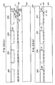
- Figs. 11A and 11B are views which illustrate a third embodiment.
- Reference numeral 202 represents an electric circuit component holding member comprising a ceramic substrate in which recessed portions in which the semiconductor devices 101 are held therein are formed. After positioning the semiconductor devices 101 within the recessed portions of the ceramic substrate 202 such that the positions of the conjunction portions 102 of the semiconductor devices 101 correspond to the positions of the conjunction portions of the circuit substrate 104, the peripheral portions are held by resin 203. Then, the ceramic substrate 202 is turned as to make the conjunction portions 102 of the semiconductor devices 101 confront the conjunction portions 105 of the circuit substrate 104, and the electrically connecting member 125 is inserted therebetween (see Fig. 11A).
- the conjunction portions of the circuit substrate 104 and the conjunction portions 109 of the electrically connecting member 125 are positioned, and then the ceramic substrate 202 and the circuit substrate 104 are positioned as to establish the connection between the conjunction portions 102 of the semiconductor devices 101 and the conjunction portions 108 of the electrically connecting member 125, connection between the conjunction portions 105 of the circuit substrate 104 and the conjunction portions 109 of the electrically connecting member 125 by metallizing and/or alloying (see Fig. 11B).
- the recessed portions in the ceramic substrate 202 can hold any type of semiconductor devices by designing the recessed portion in the form which correspond to the shape of the semiconductor devices 101a to 101d to be held.
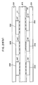
- Figs. 13A to 13D are views which illustrate a fourth embodiment.
- Reference numeral 205 represents a glass substrate for temporally fastening the semiconductor device 101 and a frame 206.
- the frame 206 is temporally fastened on the glass substrate 205 by an adhesive.
- the semiconductor devices 101 are positioned as to make the positions of the conjunction portions 102 thereof correspond to the positions of the conjunction portions of the circuit substrate 104, and then, the semiconductor devices 101 are temporally fastened to the glass substrate 104 by an adhesive (see Fig. 13A).
- the thus-manufactured electric circuit component holding member is turned as to make the conjunction portions 102 of the semiconductor devices 101 and the conjunction portions 105 of the circuit substrate 104 confront each other, and the electrically connecting member 125 is inserted therebetween (see Fig. 13C).
- the the conjunction portions 109 of the electrically connecting member 125 and the conjunction portions 105 of the circuit substrate 104 are positioned, and then, the electric circuit component holding member 208 and the circuit substrate 104 are positioned as to establish a connection between the conjunction portions 102 of the semiconductor device 101 and the conjunction portions 108 of the electrically connecting member 125 and a connection between the conjunction portions 105 of the circuit substrate 104 and the conjunction portions 109 of he electrically connecting member 125 by metallizing and/or alloying (see Fig. 13D).
- the thickness of the devices can be reduced.
- Figs. 14A and 14B are views which illustrate a fifth embodiment.
- the semiconductor devices 101 held by the glass substrate 201 with the electrically connecting members 125 are connected to the circuit substrate 104, and similarly semiconductor devices 101′ held by a glass substrate 201′ are connected to this circuit substrate 104.
- the electric circuits can be classified into units. As a result, a variety of types can be manufactured from the same manufacturing process.
- a structure may be employed such that a relief is formed in the electric circuit component holding member 201′ as to be connected to the same circuit substrate.
- a structure may be employed as shown in Figs. 16A and 16B, such that the electric circuit component holding members 201 and 201′ are disposed on the two sides of the circuit substrate 104 as to connect the semiconductor devices 101 and 101′.
- Figs. 17A and 17B are views which illustrate a sixth embodiment.
- the conjunction portions of semiconductor devices 208 which are the individual semiconductors from the semiconductors 101 and 101′ to be held by the glass substrate 201 and the conjunction portions of the electrically connecting member 125 are positioned as to be connected to the conjunction portions of the electrically connecting members 125 by metallizing and/or alloying, and this semiconductor device 208 is connected to the circuit substrate 104 by metallizing and/or alloying.
- the positions of the conjunction portions of the semiconductor devices 101 and 101′ and the positions of the conjunction portions 108 of the electrically connecting member 125 connected to the semiconductor device 208 connected to the circuit substrate 104 correspond to each other so that the semiconductor devices 101 and 101′ are held by the glass substrate 201 by an adhesive.
- the glass substrate 201 is turned as to make the positions of the conjunction portions 102 of eh semiconductor devices 101 and 101′ correspond to the positions of the conjunction portions 108 of the electrically connecting member 125.
- the glass substrate 201 and the circuit substrate 104 are positioned as to be connected to each other by metallizing and/or alloying.
- the other semiconductor devices can be readily connected to the semiconductor device and the conjunction portions exhibited an excellent reliability.
- Figs. 18A and 18B are views which illustrate a seventh embodiment.
- the semiconductor devices 101 and the circuit substrate 104 are employed as the electric circuit component and the other electric circuit components, in which the portions other than the conjunction portions are covered with insulating films 103 and 106.
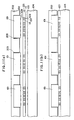
- Figs. 19A and 19B The electrically connecting member shown in Figs. 19A and 19B was used.
- Figs. 19A is a perspective view
- Fig. 19B is a cross-sectional view.
- the electrically connecting member 125 is so arranged that the portion of the metal members 107 which appear outside project over the surface of the holding body (resin insulating body) 111.
- This electrically connecting member 125 may be manufactured by, for example, the following method.
- the electrically connecting member shown in Figs. 6B and 6C is prepared.
- the two sides of this electrically connecting member are subjected to an etching to make the metal wire 121 project or the surface of the polyimide resin by substantially 10 ⁇ m.
- the length of projection of the metal wire 121 is arranged to be 10 ⁇ m according to this embodiment, it may be optionally determined.
- a method of making the metal wire 121 project is not limited to this etching. The other chemical or mechanical methods can be employed.
- Bumps 150 as shown in Figs. 20A and 20B may be formed by fitting the electrically connecting member 125 within a mold having recessed portions at the positions corresponding to the metal wire 121 to deform the projections 126 of the metal wire 121. In this case, the metal wires 121 cannot be readily separated from the insulating body 111.
- the metal wires 121 form the metal members 107 and the resin 123 forms the insulating body 111.
- the bumps may be formed by melting the projections by heat or the other methods.
- the conjunction portions also exhibited excellent reliability.
- Figs. 21A and 21B are views which illustrate an eighth embodiment.
- the electrically connecting member 125 is individually designed from that according to the seventh embodiment.
- the electrically connecting member 125 according to this embodiment is designed such that the pitch between the metal members is narrower with respect to that shown in the seventh embodiment. That is, according to this embodiment, the pitch between the metal members 107 is arranged to be narrower than the interval between the conjunction portions of the semiconductor devices.
- the electrically connecting member 125 since the conjunction portions for the electrically connecting member 125 is disposed at the positions at which the semiconductor devices 101 and the circuit substrate 104 is connected to each other, the electrically connecting member 125 needs to be positioned. According to this embodiment, although positioning between the semiconductor devices 101 and the circuit substrate 104 needs to be conducted, positioning with respect to the electrically connecting member 125 becomes needless. As a result, if the dimensions d11 and P11 for connecting the semiconductor devices 101 and the circuit substrate 104 and the dimensions d12 and P12 for connecting the electrically connecting member are determined properly, they can be connected to each other without any necessity of performing positioning.
- the conjunction portions also exhibited excellent reliability.
- the difference from the first embodiment lies in that a circuit substrate having the surface on which a circuit is formed is employed as the electric circuit component holding member 201 and the surfaces of the semiconductor devices 101 on which the one or more conjunction portions 102 are not present are held by metallizing and/or alloying or by using an adhesive.
- the circuit substrate 201, the semiconductor devices 101, electrically connecting member 125 and the circuit substrate 104 are prepared.
- the semiconductor devices 101 and the circuit substrate 104 includes a multiplicity of conjunction portions 102 and 105.
- the metal portions of the conjunction portions 102 of the semiconductor devices 101 appear outside at the positions corresponding to the conjunction portions 105 of the circuit substrate 104 and the conjunction portions 108 and 109 of the electrically connecting member 125.
- the semiconductor devices 101 are positioned to the circuit substrate 201 as to make the positions of the conjunction portions 102 of the semiconductor devices 101 correspond to the positions of the conjunction portions 105 of the circuit substrate 104. Then, the semiconductor devices 101 and the circuit substrate 201 are connected to each other by metallizing and/or alloying so that the semiconductor devices 101 are held by the circuit substrate 201.
- the semiconductor devices 101 connected to the circuit substrate 201 may be electrically insulated within the circuit substrate.
- the circuit substrate 201 is turned as to make the conjunction portions 102 of the semiconductor devices 101 and the conjunction portions of the circuit substrate 201 confront each other, and the electrically connecting member 125 is inserted therebetween (see Fig. 22A).
- a positioning is so performed that the conjunction portions 105 of the circuit substrate 104 correspond to the conjunction portions 109 of the electrically connecting member 125. Then, the circuit substrate 201 and the circuit substrate 104 are positioned. As a result, since the conjunction portions 102 of the semiconductor devices 101 held by the circuit substrate 201 are positioned such that the positions thereof correspond to the positions of the conjunction portions 105 of the circuit substrate 104 as to be held, the positions of the same are necessarily correspond to the positions of the conjunction portions 105 of the circuit substrate 104, that is the positions of the conjunction portions 108 of the electrically conductive member 125.
- connection can be established such that a connection between Al of the conjunction portions 102 of the semiconductor devices 101 and Au of the conjunction portions 108 of the electrically connecting member 125, and a connection between Au of the conjunction portions 105 of the circuit substrate 104 and Au of the conjunction portions 109 of the electrically connecting member 125 are established by metallizing and/or alloying (see Fig. 22B).
- Any method can be selected from the following three methods in order to connecting the semiconductor devices 101, the electrically connecting member 125 and the circuit substrate 104 by metallizing and/or alloying.
- the thus-manufactured electric circuit apparatus exhibited excellent reliability in the connections of the conjunction portions as a result of the examination.
- Figs. 25A to 25D are views which illustrate a tenth embodiment.
- the difference from the second embodiment lies in that a circuit substrate is employed as the electric circuit component holding member 201 and the semiconductor devices 101 are connected to the circuit substrate 201 by metallizing and/or alloying after a positioning as to make the positions of the conjunction portions 109 of the semiconductor devices 101 and the conjunction portions 105 of the circuit substrate 104 correspond to each other (see Fig. 25B).
- the conjunction portions exhibited excellent reliability. As shown in Figs. 26A and 26B, the sequential order of connection can be changed.
- Figs. 27A and 27B illustrate an eleventh embodiment.
- the semiconductor devices 101 connected to the circuit substrate 201 with the electrically connecting member by a method according to the ninth embodiment are connected to the circuit substrate 104.
- the semiconductor devices 101′ connected to the circuit substrate 201′ by a method according to the ninth embodiment are connected to this circuit substrate 104.
- the semiconductor devices 101 and 101′ serving as the electric circuit components are connected to the two sides of the circuit substrate 104 with the electrically connecting member 125.
- Figs. 29A and 29B are views which illustrate a twelfth embodiment.
- the conjunction portions of the semiconductor device 203 which is individually provided from the semiconductor devices 101 to be held by the circuit substrate 201 and the conjunction portions of the electrically connecting member 125 are positioned as to be connected to each other by metallizing and/or alloying. Then, the semiconductor devices 203 are connected to the circuit substrate 104 by metallizing and/or alloying. Next, the semiconductor devices 101 are positioned as to make the positions of the conjunction portions 102 of the semiconductor devices 101 and the conjunction portions 108 of the electrically connecting member 125 on the semiconductor device 203 connected to the circuit substrate 104 correspond to each other as desired as to be connected to the circuit substrate 201 by metallizing and/or alloying.
- the circuit substrate 201 is turned as to dispose the conjunction portions 102 of the semiconductor devices 101 to confront the conjunction portions 108 of the electrically connecting member 125 so that the circuit substrate 201 and the circuit substrate 104 are positioned. Then, the conjunction portions 102 of the semiconductor devices 101 and the conjunction portions 108 of the electrically connecting member 125 are connected to each other by metallizing and/or alloying.
- the other semiconductor devices can be readily connected to the semiconductor device.
- semiconductor devices of a type which cannot be arranged to be a monolithic type can be connected simply with a shortest length required for connection.
- the conjunction portions also exhibited excellent reliability.
- each components are electrically connected similarly to the ninth embodiment except for the difference lies in that the electrically connecting member according to the seventh embodiment is used.
- the conjunction portion exhibited excellent reliability.
- FIG. 30A and 30B A fourteenth embodiment is shown in Figs. 30A and 30B.
- the electrically connecting member 125 has uneveness in order to establish a connection between the circuit substrate 201 and 101 as not to prevent contact with the semiconductor device 101.
- the polyimide resin 111 in the portion in which the recessed portion is formed is subjected to an etching, and then, the projecting metal wire portion is subjected to an etching.
- the uneveness may be formed by layering an electrically conductive member, from which the portion corresponding to the recessed portion is cut off, on one sheet of the electrically conductive member.
- the other chemical or mechanical methods may be employed.
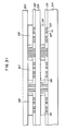
- the circuit substrate 201 serving as the electric circuit component holding member on which the circuit is formed comprises, as shown in Fig. 31, a double-sided or a multilayered double-sided substrate
- the semiconductor device 101′ and the circuit substrate 201′ can be connected to each other with the electrically connecting member 125′ by a similar method.
- the number of the layers may be determined to be one or a plurality of layers.
- a structure may be employed which is designed such that a semiconductor device 4 is formed by the conventional method on the circuit substrate 201 and the connection is established by an Au-wire 7.
- the available conventional method is exemplified by a flip chip method, a TAB method, and soldering.
- 3-D dense mounting can be performed, and the conjunction portion exhibited excellent reliability.
- the electrical connection between the subject members is established similarly to the ninth embodiment except for the difference lies in that the electrically connecting member described in the eighth embodiment.
- the conjunction portions exhibited excellent reliability.
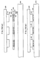
- Fig. 33A is a cross-sectional view, a state in which no connection is established between the electric circuit component holding member 201 holding a plurality of the semiconductor devices 101 serving as the electric circuit components and the electrically connecting member 125.
- the number of the semiconductor devices 101 is not limited if it exceeds one.
- the metal members 107 made of an electrically conductive material are embedded in the holding body 111 made of an organic material. End portions 108 of the metal members 107 appear outside on one sides of the holding body 111. Other end portions 109 of the metal members 107 appear outside on the other sides of the holding body 111.
- Reference numeral 101 represent semiconductor devices
- 102 represents conjunction portions of the semiconductor devices
- 201 represents a glass substrate serving as the electric circuit holding member.
- the glass substrate 201 holds at least one of the sides of the semiconductor devices 101, this at least one of the sides being the sides on which at least one of the conjunction portions 102 do not present.
- Fig. 33B is a view which illustrates a state where the semiconductor devices 101 are connected to end portions 108 of the metal members 107 which appear on one side of the holding body 111 by metallizing and/or alloying.
- reference numeral 104 represents a circuit substrate serving as the other electric circuit component and having conjunction portions 105 therein.
- the circuits substrate 104 are connected to the other end portions 109 of the metal member 107 which appear on the other sides of the holding body 111 in the conjunction portions 105 by alloying.
- Fig. 33D is a view which illustrates a state in which the whole body is integrated by means of the above-described connection.
- the semiconductor devices 101 are positioned to the glass substrate 201 as to establish the designed positional relationship between the conjunction portions 102 of the semiconductor devices 101 and the conjunction portions 105 of the circuit substrate 104 as to be held by this glass substrate 201.
- the conjunction portions 108 of the electrically connecting member 125 and the conjunction portions of the semiconductor devices 101 are positioned as to be connected to each other by metallizing and/or alloying.
- the glass substrate 201 is turned as to make the conjunction portions 102 of the semiconductor devices 101 confront the conjunction portions 105 of the circuit substrate 104.
- the glass substrate 201 and the circuit substrate 104 are positioned, and then the conjunction portions 109 of the electrically connecting member 125 and the conjunction portions 015 of the circuit substrate 104 are connected to each other by pressurization.
- the conjunction portions 109 of the electrically connecting member 125 and the conjunction portions 105 of the circuit substrate 104 are again brought to the pre-connection state. If a pressure is again applied after positioning, the connection can be established. Therefore, if a failure generates in the semiconductor devices 101 or the circuit substrate 104, the defective one is replaced by a new one with the pressure released, and the connection is again established by a pressure applied after the positioning has been performed so that an well-conditioned electric circuit apparatus can be obtained.
- the conjunction portions 102 of the semiconductor devices 101 and the conjunction portions 108 of the electrically connecting member 125 are connected to each other by metallizing and/or alloying.
- a similar effect can be obtained from a structure arranged such that the conjunction portions 015 of th circuit substrate 014 and the conjunction portions 109 of the electrically connection member 125 are connected to each other by metallizing and/or alloying, and the connection between the conjunction portions 102 of the semiconductor devices 101 and the conjunction portions 108 of the electrically connecting member 125 is established by applying a pressure.
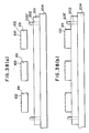
- Figs. 34A and 34B are views which illustrate a seventeenth embodiment. According to this embodiment, the portions other then the conjunction portions on one side in which the metal members 107 of the electrically connecting member 125 appear are applied with an adhesive.
- the semiconductor devices 101 After positioning the semiconductor devices 101 to the circuit substrate 201 serving as the electric circuit component holding member such that the designed positional relationship between the conjunction portions 102 of the semiconductor devices 101 and the conjunction portions 105 of the circuit substrate 104 is established, they are connected to each other and/or the semiconductor devices 101 are held by the circuit substrate 201. Then, the electrically connecting member 125 and the semiconductor devices 101 are stacked to each other after the position has been performed such that the side applied with the adhesive 202 and the side on which the conjunction portions 102 of the semiconductor devices 101 are present confront each other.
- any defective component can be readily replaced similarly to the sixteenth embodiment.
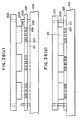
- Figs. 35A to 35C, and Figs. 36A and 36B are views which illustrate an eighteenth embodiment.
- an electrically connecting member is employed which is designed such that the metal members which appear on one side of the electrically connecting member 125 and the metal members which appear on the other side are made of material which have individual melting points.
- An electrically connecting member 125 shown in Figs. 6B and 6C is prepared by the method according to the first embodiment.
- Resists 203 are, as shown in Fig. 35A, formed by a photo-litho method in the portions in which no metal members 107 appears in one side of this electrically connecting member 125.
- a diffused barrier layer 204 made of Mo, W, Pd or the like is formed by spattering.
- An Au-Sn (20 wt%) layer is formed on this barrier layer 204 (see Fig. 35B), and the resists 203 are removed by a lift-on method (see Fig. 35C).
- the barrier layer 204 and a Pb-Ag-Sn (36.1-1.4-62.5 wt%) layer 206 are formed on the other side of the electrically connecting member.
- the thus-manufactured electrically connecting member 125 is arranged, at the two ends of the metal members 107 thereof, such that the Au-Sn (20 wt%) layer displays a melting point of 280 °C while the Pb-Ag-Sn (36.1-1.4-62.5 wt%) layer displays a melting point of 180 °C, in which the difference in the melting point becomes substantially 100 °C.
- the above-described electrically connecting member 125 is, as shown in Fig. 36, heated up to 300 °C or higher and compressed after positioning the glass substrate 201 holding the semiconductor devices 101, the electrically connecting member 125 and the circuit substrate 104.
- a connection between the conjunction portions 102 of the semiconductor devices 101 and the conjunction portions 108 of the electrically connecting member 125 and a connection between the conjunction portions 105 of the circuit substrate 104 and the conjunction portions 109 of the electrically connecting member 125 are established by simultaneously metallizing and/or alloying.
- the composition ratio can be changed due to the thermal diffusion of metal atoms whenever heating is conducted, the number of the attachment and the detachment is of course limited.
- the two conjunction portions can be connected to each other by metallizing and/or alloying, the resistance at the conjunction portions can be significantly reduced. As a result, a stable connection can be always obtained.
- the Au-Su layer 205 is formed on the end portions 108 of the metal member 107 while the Pb-Ag-Sn layer 206 is formed on the other end portions 109, it can be conducted in a reversed manner.
- an alloy layer other than that described above can be employed as the 205 and 206 if proper melting points and a proper difference in temperatures can be obtained.
- an electrical connecting between components is established similarly to the sixteenth embodiment except for the difference lies in that the electrically connecting member according to the eighth embodiment is employed.
- an electrical connecting between components is established similarly to the sixteenth embodiment except for the difference lies in that a circuit substrate on which a circuit is formed on the surface thereof is employed alternately to the glass substrate as the electric circuit component holding member.
- Figs. 33A to 33D the semiconductor devices 101 are positioned to the circuit substrate 201 such that the designed positional relationship between the conjunction portions 102 of the semiconductor devices 101 and the conjunction portions 105 of the circuit substrate 104 is established as to be connected to the circuit substrate 201 and/or to be held by the same.
- Fig. 33B after positioning the conjunction portions 108 of the electrically connecting member 125 and the conjunction portions of the semiconductor devices 101, they are connected to each other by metallizing and/or alloying.
- the circuit substrate 201 is turned as to make the conjunction portions 102 of the semiconductor devices 101 confront the conjunction portions 015 of the circuit substrate 104.
- circuit substrate 201 and the circuit substrate 104 are positioned as shown in Fig. 33D, and then the conjunction portions 109 of the electrically connecting member 125 and the conjunction portions 105 of the circuit substrate 104 are connected to each other by a pressure applied after the positioning.
- the conjunction portions 105 of the electrically connecting member 125 and the conjunction portions 109 of the circuit substrate 104 are, as shown in Fig. 33C, brought to the state before establishment of the connection.
- the connection is again established. Therefore, if a failure is generated in the semiconductor devices 101 or the circuit substrate 104, the defective one can be replaced by a new one by releasing the pressure. Then the connection is again established by applying a pressure so that an well-conditioned electric circuit apparatus can be obtained.
- conjunction portions 102 of the semiconductor devices 101 and the conjunction portions 108 of the electrically connecting member 125 are connected to each other by metallizing and/or alloying, it is apparent that a similar effect can be obtained from a structure arranged such that the conjunction portions 105 of the circuit substrate 104 and the conjunction portions 109 of the electrically connecting member 125 are connected to each other by metallizing and/or alloying and the conjunction portions 102 of the semiconductor devices 101 and the conjunction portions 108 of the electrically connecting member 125 are connected by applying a pressure.
- an electrical connecting between components is established similarly to the seventeenth embodiment except for the difference lies in that a circuit substrate on which a circuit is formed on its surface is employed as an alternative to the glass substrate as the electric circuit component holding member. Also according to this embodiment, defective components can be readily replaced.
- the composition ratio can be changed due to the thermal diffusion of metal atoms whenever heating is conducted, the number of the attachment and the detachment is of course limited.
- the two conjunction portions can be connected to each other by metallizing and/or alloying, the resistance at the conjunction portions can be significantly reduced. As a result, a stable connection can be always obtained.
- an electrical connecting between components is established similarly to the twenty first embodiment except for the difference lies in that the electrically connecting member according to the seventh embodiment is employed.
- defective components can be readily replaced and the conjunction portions exhibited excellent reliability.
- excellent reliability can be obtained in the various characteristics thereof.
- an electrical connecting between components is established similarly to the twenty first embodiment except for the difference lies in that the electrically connecting member according to the eighth embodiment is employed.
- Fig. 37 is a view which illustrates a twenty sixth embodiment.
- the electrically connecting member 125 is formed to have steps, in which the conjunctions portions of the corresponding circuit substrates 201 and 104 are connected to each other by the electrically conductive member 107 embedded in the holding body 111, and the semiconductor devices 101 connected to and/or held by the circuit substrate 207 serving as the electrically connecting member and the holding member are connected to the circuit substrate 201 so that a multilayered structure is formed.
- a cross-sectional view Fig. 38A is a view which illustrates a state before the plurality of the semiconductor devices 101 serving as the electric circuit components are connected to and/or held by the electric circuit component holding member 201.
- Reference numeral 204 represents a positioning jig and having a positioning pin 205′.
- the number of the semiconductor devices 101 may be optionally determined if it exceeds one.
- Fig. 38B is a view which illustrate a state after the semiconductor devices 1011 have been connected to and/or held by the electric circuit component holding member 201.
- Fig. 38C is a view which illustrates a state where the semiconductor devices 101 connected to and/or held by the electric circuit component holding member 201 and the circuit substrate 104 serving as the other electric circuit component are made confront each other with the electrically connecting member 125.
- the metal members 107 serving as the electrically conductive members are embedded in the holding body 111 made of an organic material, end portions of the metal members 107 appear on one side of the holding body 111, the other end portions 109 of the metal members 107 appear on the other side of the holding body 111, and positioning holes 203 are formed.
- the electric circuit component holding member 201 comprises a glass plate and holds, by an adhesion force, at least one side of each of the semiconductor devices 101 on which the at least one or more conjunction portions 102 are not present, positioning holes 202 being formed therein.
- the semiconductor devices includes conjunction portions 102 at which the semiconductor devices are connected to one end portions 108 of the metal members 107 which appear on one side of the holding body 111 by alloying.
- the circuit substrate 104 includes conjunction portions 015 at which the circuit substrate 104 are connected to the other end portions 109 of the metal members 107 which appear on the other side of the holding body 11 by alloying, positioning pins being formed therein.
- Fig. 38D is a cross-sectional view which illustrates a state in which the above-described components are integrated by the connection.
- the positioning holes 202 and 203 and the positioning pins 205 are the mechanical portions or the functionating portions which serve as reference for the positional relationship.
- the semiconductor devices 101 are, by using the positioning pins 205′ as the references, positioned as to establish a designed positional relationship between the conjunction portions 102 of the semiconductor devices 101 and the conjunction portions 105 of the circuit substrate 104 as to be held by the glass substrate 201 by an adhesive.
- the semiconductor devices 101 are positioned as to establish a designed positional relationship between the conjunction portions 102 and the conjunction portions of the circuit substrate 104 to be held with an adhesive (see Fig. 38A and 38B).
- the thus-manufactured electric circuit component holding member 201 is removed from the holding position determining jig 204, and then the electrically connecting member 125 and the circuit substrate 104 are prepared.
- Each of the semiconductor devices 101 and the circuit substrate 104 according to this embodiment includes a plurality of the conjunction portions 102 and 104.
- the conjunction portions 102 of he semiconductor devices 101 are arranged such that the metal appears at the positions which correspond to the conjunction portions 105 of the circuit substrate 104 and the conjunction portions 108 and 109 of the electrically connecting member 125.
- the positioning pins 205 provided for the circuit substrate 104 are inserted into the positioning holes 203 formed in the electrically connecting member 125, and then these positioning pins 205 are inserted into the positioning holes 202 formed in the electric circuit component holding member 201 so that the positioning is completed. Then, as shown in Fig. 38, a connection between Al of the conjunction portions 102 of the semiconductor devices 101 and Au fo the conjunction portions 108 of the electrically connecting member 125 and a connection between Au of the conjunction portions of the circuit substrate 104 and Au of the conjunction portions of the electrically connecting member 125 are established by metallizing and/or allying.
- any of the following three methods can be employed to connect the semiconductor devices 101, the electrically connecting member 125, and the circuit substrate 104 by metallizing and/or alloying.
- the position pins 205 are provided for the circuit substrate 104, it is apparent that a similar effect can be obtained even if the same is provided for the glass substrate 201 which serves as the electric circuit holding member.
- a structure may be employed which is arranged such that positioning holes are formed in both the glass substrate 201 serving as the electric circuit holding member and the circuit substrate 104 and the positioning pins are provided for both the same.
- a similar effect can be obtained from a structure arranged such that the positioning holes are formed in both the glass substrate and the circuit substrate but the positioning pins are not provided for the same.
- the positioning pins are provided for the connecting position determining jig similarly to the manner in which the pins are provided for the holding position determining jig used in Figs. 38A and 38B.
- positioning marks may be provided for the circuit substrate as to perform the positioning required at the connection such that the positioning marks are present within the positioning holes formed in the electric circuit component holding member.
- the electric circuit component holding member is made of a light transmissible material by arranging the structure such that light can pass through only the positioning holes as an alternative to forming the holes.
- Figs. 41A to 41D are views which illustrate a twenty-eighth embodiment.
- reference numeral 206 represents a reference plane of the circuit component holding member
- 207 represents a reference plane of the circuit substrate 104.
- These reference planes 206 and 207 are the mechanism portion or the functionating portion which serves as the reference for clarifying the positional relationship.
- the semiconductor devices 101 are positioned to the reference plane 206 Of the electric circuit component holding member 201 such that the designed positional relationship between the conjunction portions 102 of the semiconductor devices 101 and the conjunction portions 105 of the circuit substrate 104 is established as to be held by the electric circuit component holding member 021. Then, the electric circuit component holding member 201 is turned as to make the conjunction portions 012 of the semiconductor devices 101 and the conjunction portions 105 of the circuit substrate 104 confront each other, and the reference plane 206 of the electric circuit component holding member 201 is abutted to the reference plane 207 of the circuit substrate 104 as to be positioned. Then the conjunction portions 102 of the semiconductor devices 101 and the conjunction portion of the circuit substrate 104 are connected to each other by metallizing and/or alloying>
- the reference plane 206 of the electric circuit component holding member 201 is arranged in the form of a projection shape, a similar effect can be obtained from a structure arranged such that the projecting reference plane is, on the contrary, provided on the circuit substrate 104. If two or more reference planes are provided, the positioning can be completed simply by one abutting.
- a reference plane abutting portion 208 is provided for the holding position determining jig 204 as to position and hold the semiconductor devices 101 by abutting the electric circuit component holding member 201. Then, both the circuit substrate and the electric circuit component holding member are abutted against a reference plate abutting portion 210 provided for the connection position determining jig 209 as to perform the positioning and establish the connection.
- an electrical connection between components is established similarly to the twenty seventh embodiment except for the difference lies in that the electrically connecting member according to the seventh embodiment is employed.
- the conjunction portions exhibited excellent reliability.
- an electrical connection between components is established similarly to the twenty seventh embodiment except for the difference lies in that the electrically connecting member according to the eighth embodiment is employed.
- the conjunction portions exhibited excellent reliability.
- Fig. 43A is a cross-sectional view which illustrates a state in which the plurality of the semiconductor devices 101 serving as the electric circuit components are held by the electric circuit component holding member 201.
- the semiconductor devices 101 includes the conjunction portions 102.
- the number of the semiconductor devices 101 needs to be one or more.
- a projection portions 201′ is provided on the peripheral portion of the electric circuit component holding member 201 so that the overall contour is formed in a cap-like shape.
- Fig. 43B is a view which illustrates a state where the semiconductor devices 101 held by the electric circuit component holding member 201 and the circuit substrate 104 serving as the other electric circuit component are made confront each other with the electrically connecting member 125.
- the metal members 107 serving as the electrically conductive members are embedded in the holding body 111 made of an organic material, and end portions of the metal members 107 appear on one side of the holding body 111 while the other end portions 109 of the metal members 107 appear on the other side of the holding body 111.
- the electric circuit component holding member 201 is made of ceramics, and it holds, with an adhesion force, at least one side of each of the semiconductor devices 101 on which at least one conjunction portions 102 are not present, this electric circuit component holding member 201 serving as well a function of a cap.
- the semiconductor devices 101 including the conjunction portions 102 at which the semiconductor devices 101 are connected to the one end portions 108 of the metal members 107 which appear on one side of the holding body 111 by alloying.
- the circuit substrate 104 includes the conjunction portion 105 at which the circuit substrate 104 is connected to the other end portions 109 of the metal members 107 which appear on the other side of the holding body 111 by alloying.
- Epoxy resin 202 is applied to the circuit substrate 104 in the portion which confronts the sealing projection portion 201′ of the electric circuit component holding member 201.
- Fig. 43C is a cross-sectional view which illustrates a state in which the overall body is integrated by the above-described connection and the semiconductor devices 101 are simultaneously sealed by the electric circuit component member 201.
- the semiconductor devices 101 are positioned to the electric circuit component holding member 201 as to realize the designed positional relationship between the conjunction portions 102 of the semiconductor devices 101 and the conjunction portions 105 of the circuit substrate 104 as to be held by the electric circuit component holding member 201 by using an adhesive.
- the electric circuit component holding member 201 is turned as to make the conjunction portions 102 of the semiconductor devices 101 confront the conjunction portions 015 of the circuit substrate 104, and the electrically connecting member 125 is inserted therebetween (see Fig. 43B).
- a positioning is performed such that the conjunction portions 102 of the semiconductors 101 held by the electric circuit component holding member 201 and end portions 10B of the electrically conductive member 125 confront each other and the positions of the conjunction portions 105 of the circuit substrate 104 and the positions of the conjunction portions of the electrically connecting member 125 correspond to each other.
- the circuit substrate 104 is applied with epoxy resin 202 in the portions thereof which confronts the sealing projections 201′ disposed on the peripheral portion of the electric circuit component holding member 201.
- a connection between Al of the conjunction portions 102 of the semiconductor devices 101 and Au of the conjunction portions 108 of the electrically connecting member 125 and a connection between Au of the conjunction portions 105 of the circuit substrate 104 and Au of the conjunction portions 109 of the electrically connecting member 125 are established by metallizing and/or alloying (see Fig. 43C).
- the sealing projection 201′ disposed on the periphery of the electric circuit component holding member 201 is simultaneously brought into contact with the epoxy resin 202 so that the portion between the sealing projection 201′ and the circuit substrate 104 is perfectly enclosed by the epoxy resin by the pressure applied due to the connecting action.
- the thus-applied epoxy resin 202 is hardened, and the sealing is completed.
- any of the following three methods can be employed to connect the semiconductor devices 101, the electrically connecting member 125 and the circuit substrate 104 by metallizing and/or alloying.
- the thus-manufactured electric circuit apparatus exhibited reliable connection in the conjunction portions as a result of the examination.
- the sealing projections 201′ at the peripheral portion of the electric circuit component holding member 201 vertically comes contact with the circuit substrate.
- An additional sealing effect can be obtained and reliability can be improved by arranging the shape of the sealing projection 201′ in an L-shape to increase the area of contact.
- similar sealing can be conducted even if the resin 202 is brought to a higher position by a frame 203 provided for the circuit substrate 104 and the shape of the electric circuit component holding member 201 is designed to intact be a flat shape.
- Figs. 45A and 45B are views which illustrate a thirty-second embodiment.
- Fig. 45A is a cross-sectional view which illustrates a state before the connection between the semiconductor devices 101 serving as the electric circuit component held by the electric circuit component holding member 201 and the circuit substrate 104 serving as the other electric circuit component is established.
- the shape of the electric circuit component holding member 201 is the same as that of the member according to the twenty-second embodiment.
- the semiconductor devices 101 includes conjunction portions 102 and are held by the electric circuit component holding member 201 after positioning.
- the circuit substrate 104 includes conjunction portions 105 in which recessed portions 104′ into which the sealing projection 201′ of the holding member 201 is fitted are formed.
- the recessed portions 104 is arranged to be filled with the resin 202.
- the recessed portion 104′ is formed in the circuit substrate 104, the pressure due to establishing connecting is applied only to the semiconductor devices 101. As a result, connection can be strongly performed, and since the water invasion route within the sealing portion comprising the recessed portions 201′ and 104′ toward the inside portion of the apparatus can be elongated, causing reliability to be improved.
- an electrical connection between components is established similarly to the thirty-first embodiment except for the difference lies in that the electrically connecting member according to the seventh embodiment is employed.
- the conjunction portions exhibited excellent reliability, and excellent reliability in the various characteristics was obtained.
- an electrical connection between components is established similarly to the thirty-first embodiment except for the difference lies in that the electrically connecting member according to the eighth embodiment is employed.
- the conjunction portions exhibited excellent reliability.
- a reliable connection can be obtained in the connection of the electric circuit parts such as connection of the semiconductor devices and the circuit substrates and/or lead frames. Therefore, the conventional methods such as a wire bonding method, a TAB method, and a CCB method and the like can be replaced by the method according to the present invention.
- the conjunction portions of the electric circuit parts can be disposed at any positions desired (particularly in the inner portion). Therefore, a further great number of contacts can be used for the connection with respect to the conventional wire bonding method or the TAB method. Therefore, a system suitable for multi-pin connection can be obtained.
- an insulating material is previously present in the neighboring metals of the electrically conjunction members, electric conduct between the neighboring metals can be prevented. Therefore, a further great number of contacts can be employed with respect to the CCB method.
- the holding body of the electrically connecting member is arranged such that the insulating body thereof is made of either power or fiber or a material obtained by dispersing both the powder and fiber comprising one or a plurality of metals or inorganic materials exhibiting excellent heat conductivity or the insulating body is made of a metal or an inorganic material whose electrically conductive member can be insulated, heat from the electric circuit components can be discharged though the electrically connecting member or the other electric circuit components. Therefore, an electric circuit apparatus exhibiting excellent heat discharging performance can be obtained.
- the electric circuit component holding member is formed by sole type of metal or an inorganic material exhibiting excellent heat conductivity, heat from the electric circuit components can be discharge through the electric circuit component holding member. As a result, an electric circuit apparatus exhibiting excellent heat discharging performance can be obtained.
- the shape of the holding member can be designed to correspond to the electric circuit component to be held. Therefore, the connection can be performed regardless of the size, shape, and the type of the electric circuit component can be performed. Therefore, free and dense mounting can be achieved, causing a free design to be performed.
- the electric circuit components or the other electric circuit components held by or connected to the electric circuit component holding member exhibiting excellent characteristics can be again introduced into the process of manufacturing the electric circuit apparatus even if it is determined as defective at the inspection after the production of the electric circuit apparatus. As a result, manufacturing yield can be improved and manufacturing cost can be reduced.
- connection Since the connection can be collectively performed, the more the number of the connecting portions increases, the more reliable connection can be obtained in a short time.
- each positioning between the electric circuit component holding member and the electric circuit components, between the electric circuit component holding member and the other electric circuit components, or between the electric circuit component holding member, the electrically connecting member and the other electric circuit components can be performed with an addition precision obtained. That is, the positioning between the conjunction portions of the electric circuit components held or connected to the electric circuit component holding member or the position between the same and the electrically conductive members which appear on the two sides of the electrically connecting member can be performed precisely. Therefore, further precise and wide connection can be performed. The advantage of its reduced positional error will dedicate to improve the reliability since the area of connection is maintained constant.
- the electric circuit components can be connected without any necessity of performing special positioning.
- the electric circuit component holding member is as well used as a cap, the number of the required parts can be reduced, and the number of the required manufacturing processes can be reduced since the sealing can be performed at the time of performing the connection. As a result, the cost can be significantly reduced.
- An electric circuit apparatus characterized in that the same comprising: an electrically connecting member including a holding body made of an electrically insulating material and a plurality of electrically conductive members embedded in the holding body, wherein end portions of the electrically conductive members appear outside on one side of the holding body while the other end portions of the electrically conductive members appear outside on the other side of the holding body; a plurality of electric circuit components a to which the one end portions of the electrically conductive members are connected; a holding member which holds plurality of the electric circuit components a ; and another electric circuit component b to which the other end portions of the electrically conductive members are connected.
Landscapes
- Wire Bonding (AREA)
Applications Claiming Priority (12)
| Application Number | Priority Date | Filing Date | Title |
|---|---|---|---|
| JP133136/88 | 1988-05-30 | ||
| JP63133137A JPH01302735A (ja) | 1988-05-30 | 1988-05-30 | 電気回路装置 |
| JP63133136A JPH01302734A (ja) | 1988-05-30 | 1988-05-30 | 電気回路装置 |
| JP133137/88 | 1988-05-30 | ||
| JP63133393A JP2513783B2 (ja) | 1988-05-31 | 1988-05-31 | 電気回路装置 |
| JP133394/88 | 1988-05-31 | ||
| JP133393/88 | 1988-05-31 | ||
| JP63133394A JPH01302828A (ja) | 1988-05-31 | 1988-05-31 | 電気回路装置 |
| JP133392/88 | 1988-05-31 | ||
| JP63133392A JPH01302826A (ja) | 1988-05-31 | 1988-05-31 | 電気回路装置 |
| JP133391/88 | 1988-05-31 | ||
| JP63133391A JPH01302825A (ja) | 1988-05-31 | 1988-05-31 | 電気回路装置 |
Publications (3)
| Publication Number | Publication Date |
|---|---|
| EP0344702A2 true EP0344702A2 (fr) | 1989-12-06 |
| EP0344702A3 EP0344702A3 (en) | 1990-07-25 |
| EP0344702B1 EP0344702B1 (fr) | 1996-03-13 |
Family
ID=27552809
Family Applications (1)
| Application Number | Title | Priority Date | Filing Date |
|---|---|---|---|
| EP89109709A Expired - Lifetime EP0344702B1 (fr) | 1988-05-30 | 1989-05-30 | Appareil à circuit électronique |
Country Status (2)
| Country | Link |
|---|---|
| EP (1) | EP0344702B1 (fr) |
| DE (1) | DE68925922T2 (fr) |
Cited By (7)
| Publication number | Priority date | Publication date | Assignee | Title |
|---|---|---|---|---|
| DE4128603A1 (de) * | 1990-08-30 | 1992-03-05 | Micron Technology Inc | Halbleiteranordnung |
| EP0490125A1 (fr) * | 1990-11-20 | 1992-06-17 | Sumitomo Electric Industries, Ltd. | Procédé pour le montage d'éléments semiconducteurs |
| EP0560072A3 (fr) * | 1992-03-13 | 1993-10-06 | Nitto Denko Corporation | Film adhésif anisotropiquement électroconducteur et structure de connexion l'utilisant |
| US5315486A (en) * | 1991-12-16 | 1994-05-24 | General Electric Company | Hermetically packaged HDI electronic system |
| EP0762495A3 (fr) * | 1995-08-30 | 1997-08-13 | Hewlett Packard Co | Interface thermique d'un dissipateur de chaleur pour des puces montées sur un substrat |
| FR2766967A1 (fr) * | 1997-07-31 | 1999-02-05 | Scps | Dispositif de dissipation thermique et/ou protection electromagnetique pour cartes et composants electroniques |
| FR2877142A1 (fr) * | 2004-10-21 | 2006-04-28 | Commissariat Energie Atomique | Procede de transfert d'au moins un objet de taille micrometrique ou millimetrique au moyen d'une poignee en polymere. |
Family Cites Families (7)
| Publication number | Priority date | Publication date | Assignee | Title |
|---|---|---|---|---|
| US4417777A (en) * | 1981-10-13 | 1983-11-29 | Molex Incorporated | Integrated circuit carrier assembly |
| KR900001273B1 (ko) * | 1983-12-23 | 1990-03-05 | 후지쑤 가부시끼가이샤 | 반도체 집적회로 장치 |
| US4597617A (en) * | 1984-03-19 | 1986-07-01 | Tektronix, Inc. | Pressure interconnect package for integrated circuits |
| JPS6292342A (ja) * | 1985-10-17 | 1987-04-27 | Mitsubishi Electric Corp | 表面実装用半導体パツケ−ジ |
| AU598253B2 (en) * | 1986-05-07 | 1990-06-21 | Digital Equipment Corporation | System for detachably mounting semi-conductors on conductor substrates |
| EP0284820A3 (fr) * | 1987-03-04 | 1989-03-08 | Canon Kabushiki Kaisha | Pièce de connexion électrique et pièce de circuit électrique et dispositif de circuit électrique comprenant la pièce de connexion |
| US4926241A (en) * | 1988-02-19 | 1990-05-15 | Microelectronics And Computer Technology Corporation | Flip substrate for chip mount |
-
1989
- 1989-05-30 EP EP89109709A patent/EP0344702B1/fr not_active Expired - Lifetime
- 1989-05-30 DE DE68925922T patent/DE68925922T2/de not_active Expired - Fee Related
Cited By (11)
| Publication number | Priority date | Publication date | Assignee | Title |
|---|---|---|---|---|
| DE4128603A1 (de) * | 1990-08-30 | 1992-03-05 | Micron Technology Inc | Halbleiteranordnung |
| EP0490125A1 (fr) * | 1990-11-20 | 1992-06-17 | Sumitomo Electric Industries, Ltd. | Procédé pour le montage d'éléments semiconducteurs |
| AU640537B2 (en) * | 1990-11-20 | 1993-08-26 | Sumitomo Electric Industries, Ltd. | Method of mounting semiconductor elements |
| US5244142A (en) * | 1990-11-20 | 1993-09-14 | Sumitomo Electric Industries, Ltd. | Method of mounting semiconductor elements |
| US5348214A (en) * | 1990-11-20 | 1994-09-20 | Sumitomo Electric Industries, Ltd. | Method of mounting semiconductor elements |
| US5315486A (en) * | 1991-12-16 | 1994-05-24 | General Electric Company | Hermetically packaged HDI electronic system |
| EP0560072A3 (fr) * | 1992-03-13 | 1993-10-06 | Nitto Denko Corporation | Film adhésif anisotropiquement électroconducteur et structure de connexion l'utilisant |
| US5438223A (en) * | 1992-03-13 | 1995-08-01 | Nitto Denko Corporation | Anisotropic electrically conductive adhesive film and connection structure using the same |
| EP0762495A3 (fr) * | 1995-08-30 | 1997-08-13 | Hewlett Packard Co | Interface thermique d'un dissipateur de chaleur pour des puces montées sur un substrat |
| FR2766967A1 (fr) * | 1997-07-31 | 1999-02-05 | Scps | Dispositif de dissipation thermique et/ou protection electromagnetique pour cartes et composants electroniques |
| FR2877142A1 (fr) * | 2004-10-21 | 2006-04-28 | Commissariat Energie Atomique | Procede de transfert d'au moins un objet de taille micrometrique ou millimetrique au moyen d'une poignee en polymere. |
Also Published As
| Publication number | Publication date |
|---|---|
| DE68925922T2 (de) | 1996-09-05 |
| DE68925922D1 (de) | 1996-04-18 |
| EP0344702A3 (en) | 1990-07-25 |
| EP0344702B1 (fr) | 1996-03-13 |
Similar Documents
| Publication | Publication Date | Title |
|---|---|---|
| US5283468A (en) | Electric circuit apparatus | |
| US6846700B2 (en) | Method of fabricating microelectronic connections using masses of fusible material | |
| US4876588A (en) | Semiconductor device having ceramic package incorporated with a heat-radiator | |
| US6104087A (en) | Microelectronic assemblies with multiple leads | |
| US6111324A (en) | Integrated carrier ring/stiffener and method for manufacturing a flexible integrated circuit package | |
| EP0502887B1 (fr) | Boitier metallique a reseau de broches, etancheise par polymere dielectrique | |
| US5144412A (en) | Process for manufacturing plastic pin grid arrays and the product produced thereby | |
| US6084292A (en) | Lead frame and semiconductor device using the lead frame | |
| US20010048591A1 (en) | Microelectronics component with rigid interposer | |
| EP0704895A2 (fr) | Procédé de fabrication d'un dispositif semi-conducteur et d'un substrat semi-conducteur | |
| US20030011064A1 (en) | Enhanced thermal dissipation integrated circuit package and method of manufacturing enhanced thermal dissipation integrated circuit package | |
| US20180040487A1 (en) | Manufacturing method of semiconductor device and semiconductor device | |
| US8008760B2 (en) | Integrated semiconductor device | |
| CN1988138A (zh) | 高性能可再加工散热器和封装结构及其制造方法 | |
| US10109606B2 (en) | Remapped packaged extracted die | |
| US6335271B1 (en) | Method of forming semiconductor device bump electrodes | |
| EP0344702A2 (fr) | Appareil à circuit électronique | |
| US10177054B2 (en) | Method for remapping a packaged extracted die | |
| JP2023126980A (ja) | 電気めっきされたダイ取り付けを備える半導体デバイス | |
| US20020086515A1 (en) | Method of manufacturing bump electrodes and a method of manufacturing a semiconductor device | |
| US6114760A (en) | Ball grid array (BGA) semiconductor package member | |
| JPH08279591A (ja) | 半導体装置とその製造方法 | |
| EP0361715A1 (fr) | Fixation sous vide de pastilles de circuits integrés | |
| KR20020007175A (ko) | 반도체 장치 및 그 제조 방법 | |
| US20010013655A1 (en) | Methods of making microelectronic connections with liquid conductive elements |
Legal Events
| Date | Code | Title | Description |
|---|---|---|---|
| PUAI | Public reference made under article 153(3) epc to a published international application that has entered the european phase |
Free format text: ORIGINAL CODE: 0009012 |
|
| AK | Designated contracting states |
Kind code of ref document: A2 Designated state(s): DE FR GB IT NL |
|
| PUAL | Search report despatched |
Free format text: ORIGINAL CODE: 0009013 |
|
| AK | Designated contracting states |
Kind code of ref document: A3 Designated state(s): DE FR GB IT NL |
|
| 17P | Request for examination filed |
Effective date: 19901210 |
|
| 17Q | First examination report despatched |
Effective date: 19921006 |
|
| GRAA | (expected) grant |
Free format text: ORIGINAL CODE: 0009210 |
|
| AK | Designated contracting states |
Kind code of ref document: B1 Designated state(s): DE FR GB IT NL |
|
| PG25 | Lapsed in a contracting state [announced via postgrant information from national office to epo] |
Ref country code: IT Free format text: LAPSE BECAUSE OF FAILURE TO SUBMIT A TRANSLATION OF THE DESCRIPTION OR TO PAY THE FEE WITHIN THE PRE;WARNING: LAPSES OF ITALIAN PATENTS WITH EFFECTIVE DATE BEFORE 2007 MAY HAVE OCCURRED AT ANY TIME BEFORE 2007. THE CORRECT EFFECTIVE DATE MAY BE DIFFERENT FROM THE ONE RECORDED.SCRIBED TIME-LIMIT Effective date: 19960313 Ref country code: NL Free format text: LAPSE BECAUSE OF FAILURE TO SUBMIT A TRANSLATION OF THE DESCRIPTION OR TO PAY THE FEE WITHIN THE PRESCRIBED TIME-LIMIT Effective date: 19960313 |
|
| REF | Corresponds to: |
Ref document number: 68925922 Country of ref document: DE Date of ref document: 19960418 |
|
| ET | Fr: translation filed | ||
| NLV1 | Nl: lapsed or annulled due to failure to fulfill the requirements of art. 29p and 29m of the patents act | ||
| PLBE | No opposition filed within time limit |
Free format text: ORIGINAL CODE: 0009261 |
|
| STAA | Information on the status of an ep patent application or granted ep patent |
Free format text: STATUS: NO OPPOSITION FILED WITHIN TIME LIMIT |
|
| 26N | No opposition filed | ||
| REG | Reference to a national code |
Ref country code: GB Ref legal event code: IF02 |
|
| PGFP | Annual fee paid to national office [announced via postgrant information from national office to epo] |
Ref country code: FR Payment date: 20030508 Year of fee payment: 15 |
|
| PGFP | Annual fee paid to national office [announced via postgrant information from national office to epo] |
Ref country code: GB Payment date: 20030528 Year of fee payment: 15 |
|
| PGFP | Annual fee paid to national office [announced via postgrant information from national office to epo] |
Ref country code: DE Payment date: 20030612 Year of fee payment: 15 |
|
| PG25 | Lapsed in a contracting state [announced via postgrant information from national office to epo] |
Ref country code: GB Free format text: LAPSE BECAUSE OF NON-PAYMENT OF DUE FEES Effective date: 20040530 |
|
| PG25 | Lapsed in a contracting state [announced via postgrant information from national office to epo] |
Ref country code: DE Free format text: LAPSE BECAUSE OF NON-PAYMENT OF DUE FEES Effective date: 20041201 |
|
| GBPC | Gb: european patent ceased through non-payment of renewal fee | ||
| PG25 | Lapsed in a contracting state [announced via postgrant information from national office to epo] |
Ref country code: FR Free format text: LAPSE BECAUSE OF NON-PAYMENT OF DUE FEES Effective date: 20050131 |
|
| REG | Reference to a national code |
Ref country code: FR Ref legal event code: ST |