EP0345162B1 - Integrierte Vorrichtung in Halbleiterscheibengrösse - Google Patents
Integrierte Vorrichtung in Halbleiterscheibengrösse Download PDFInfo
- Publication number
- EP0345162B1 EP0345162B1 EP89401508A EP89401508A EP0345162B1 EP 0345162 B1 EP0345162 B1 EP 0345162B1 EP 89401508 A EP89401508 A EP 89401508A EP 89401508 A EP89401508 A EP 89401508A EP 0345162 B1 EP0345162 B1 EP 0345162B1
- Authority
- EP
- European Patent Office
- Prior art keywords
- wafer
- chips
- real
- lines
- scale integration
- Prior art date
- Legal status (The legal status is an assumption and is not a legal conclusion. Google has not performed a legal analysis and makes no representation as to the accuracy of the status listed.)
- Expired - Lifetime
Links
Images



Classifications
-
- H—ELECTRICITY
- H10—SEMICONDUCTOR DEVICES; ELECTRIC SOLID-STATE DEVICES NOT OTHERWISE PROVIDED FOR
- H10D—INORGANIC ELECTRIC SEMICONDUCTOR DEVICES
- H10D84/00—Integrated devices formed in or on semiconductor substrates that comprise only semiconducting layers, e.g. on Si wafers or on GaAs-on-Si wafers
-
- H—ELECTRICITY
- H10—SEMICONDUCTOR DEVICES; ELECTRIC SOLID-STATE DEVICES NOT OTHERWISE PROVIDED FOR
- H10W—GENERIC PACKAGES, INTERCONNECTIONS, CONNECTORS OR OTHER CONSTRUCTIONAL DETAILS OF DEVICES COVERED BY CLASS H10
- H10W20/00—Interconnections in chips, wafers or substrates
- H10W20/40—Interconnections external to wafers or substrates, e.g. back-end-of-line [BEOL] metallisations or vias connecting to gate electrodes
- H10W20/41—Interconnections external to wafers or substrates, e.g. back-end-of-line [BEOL] metallisations or vias connecting to gate electrodes characterised by their conductive parts
- H10W20/427—Power or ground buses
-
- G—PHYSICS
- G11—INFORMATION STORAGE
- G11C—STATIC STORES
- G11C29/00—Checking stores for correct operation ; Subsequent repair; Testing stores during standby or offline operation
- G11C29/006—Checking stores for correct operation ; Subsequent repair; Testing stores during standby or offline operation at wafer scale level, i.e. wafer scale integration [WSI]
-
- G—PHYSICS
- G11—INFORMATION STORAGE
- G11C—STATIC STORES
- G11C5/00—Details of stores covered by group G11C11/00
- G11C5/06—Arrangements for interconnecting storage elements electrically, e.g. by wiring
- G11C5/063—Voltage and signal distribution in integrated semi-conductor memory access lines, e.g. word-line, bit-line, cross-over resistance, propagation delay
-
- H—ELECTRICITY
- H10—SEMICONDUCTOR DEVICES; ELECTRIC SOLID-STATE DEVICES NOT OTHERWISE PROVIDED FOR
- H10W—GENERIC PACKAGES, INTERCONNECTIONS, CONNECTORS OR OTHER CONSTRUCTIONAL DETAILS OF DEVICES COVERED BY CLASS H10
- H10W72/00—Interconnections or connectors in packages
-
- H—ELECTRICITY
- H10—SEMICONDUCTOR DEVICES; ELECTRIC SOLID-STATE DEVICES NOT OTHERWISE PROVIDED FOR
- H10W—GENERIC PACKAGES, INTERCONNECTIONS, CONNECTORS OR OTHER CONSTRUCTIONAL DETAILS OF DEVICES COVERED BY CLASS H10
- H10W72/00—Interconnections or connectors in packages
- H10W72/50—Bond wires
-
- H—ELECTRICITY
- H10—SEMICONDUCTOR DEVICES; ELECTRIC SOLID-STATE DEVICES NOT OTHERWISE PROVIDED FOR
- H10W—GENERIC PACKAGES, INTERCONNECTIONS, CONNECTORS OR OTHER CONSTRUCTIONAL DETAILS OF DEVICES COVERED BY CLASS H10
- H10W72/00—Interconnections or connectors in packages
- H10W72/50—Bond wires
- H10W72/541—Dispositions of bond wires
- H10W72/547—Dispositions of multiple bond wires
- H10W72/5473—Dispositions of multiple bond wires multiple bond wires connected to a common bond pad
-
- H—ELECTRICITY
- H10—SEMICONDUCTOR DEVICES; ELECTRIC SOLID-STATE DEVICES NOT OTHERWISE PROVIDED FOR
- H10W—GENERIC PACKAGES, INTERCONNECTIONS, CONNECTORS OR OTHER CONSTRUCTIONAL DETAILS OF DEVICES COVERED BY CLASS H10
- H10W72/00—Interconnections or connectors in packages
- H10W72/50—Bond wires
- H10W72/551—Materials of bond wires
- H10W72/552—Materials of bond wires comprising metals or metalloids, e.g. silver
- H10W72/5524—Materials of bond wires comprising metals or metalloids, e.g. silver comprising aluminium [Al]
Definitions
- the present invention relates to a wafer scale integration (WSI) device, more particularly, to a wafer scale integration device using a bonding wire for supplying power supply voltages or common signals to a plurality of chips formed on the wafer.
- WMI wafer scale integration
- the wafer scale integration device is used for instance for a memory or a logic circuit.
- a power supply line is formed by bonding wires, since the power supply line should have low impedance characteristics and a bonding wire has low impedance characteristics.
- the bonding wire is not only used for the power supply line, but also a common signal line which requires low impedance characteristics.
- a wafer scale integration device which is used for a memory or a logic circuit, has been developed and prototype devices have been provided.
- the wafer scale integration device a plurality of circuits are integrated in all regions of the wafer.
- a wafer scale memory device which is one kind of a wafer scale integration device
- a wafer includes an array of chips each having a memory circuit and additional control logic circuit.
- a larger scale circuit can be integrated on the wafer than any other large scale integrated circuit (LSI).
- LSI large scale integrated circuit
- a signal delay time can be shortened, since a mutual wiring distance between circuits becomes shorter by integrating a system on one piece of wafer.
- a reliability of the system can be improved by compensating defective chips of the wafer or defective portions in the chip, and a reliability of mounting can be improved by decreasing assembling processes.
- the wafer scale integration device is suitable for constituting a monolithic memory or a repeated logical circuit including a plurality of basic configurations.
- a circuit should be integrated in all regions in the wafer which may include defective portions, and thus the method of constituting the system by providing redundancy and bypassing the defective chips of the wafer or defective portions of the chip becomes indispensable to increase the effective production yield to a practical level.
- each of the X-direction and Y-direction between neighboring chips are connected by local lines.
- chip here is used to mean a unit for forming a unit functional block like a unit memory block which is formed on a wafer to occupy a separate unit area and is connectable to an adjacent one by a conductor pattern and/or a wire, but is not used to mean a physically independent unit severed from a wafer.
- the wafer is cut into a square shape by cutting along the X-direction and Y-direction at the periphery thereof except for the corners, and the cut wafer is mounted on a base member called a carrier for actual use. Further, as known by persons with ordinary skill in the art, the operative chips are connected in serial bypassing defective chips, in a construction called a SPIRAL path.
- a wafer-scale multi-processor circuit based on switch lattice inter-connection scheme is discussed in a paper by K.S. Hedlund, published in Proceedings of the IEEE International Conference on Computer Design : VLSI in Computers, ICCD' 85, New York, 7th - 10th October, 1985, pages 665-671, IEEE, New-York, US.
- the wafer contains a grid of building blocks patterned in a central area, while a substantial amount of wafer space is left for the large number of interconnections required. Redundant drivers guarantee the integrity of the connections.
- a wafer-scale integration device disclosed in GB-A-2 178 204 teaches a wiring scheme to connect Vdd and Vss power lines to various modules by wire bonds from peripheral pads such as to achieve non-simultaneous refresh of the different circuit modules.
- Embodiments of the invention, as defined in claim 3, allow easy cutting of the wafer so as not to cause problems in the future.
- Figure 1 is a plane view for explaining a configuration of a wafer used for a wafer scale integration device.
- reference 1 denotes a wafer
- 1A denotes an orientation flat
- 2 denotes a chip
- 3 denotes a metal film.
- a metal film 3 which is indicated by a sand pattern, remains at some portions in the circumference of the wafer 1. These portions of the metal film are deposited in the sputtering process for forming electrode wiring, which remains in a processing stage of patterning without being eliminated, because a reticle for providing a pattern cannot be shot at some portions in the surrounding areas of the wafer due to the relationship of a stepper in an exposure apparatus, and a positive type resist is used for a photo resist.
- This metal film 3 remains after cutting the wafer 1 for mounting on the carrier, and a problem which will be described below arises due to the remaining metal film 3.
- FIG. 2 is a plane view showing cutting of the wafer shown in Fig. 1.
- reference 4 denotes power supply lines each consisting of power supply lines of Vcc and Vss.
- These power supply lines 4 are bonding wires made of, for example, aluminium, and the bonding wires are formed by using a stitch bonding technique. In the stitch bonding technique, the bonding wire can be continuously bonded to a metal pad formed on each chip without cutting the bonding wire.
- power supply lines 4 which are Vcc lines or Vss lines are constituted by bonding wires instead of the metal wiring formed on the wafer, a potential drop in the supply voltage will not be caused by low impedance characteristics of each of the bonding wires. Namely, all chips connected with the bonding wires are supplied with sufficient power supply voltages.
- the metal film 3 remains at the corner portions and the orientation flat 1A, and the power supply lines 4 may be short-circuited by the remaining metal film 3. Namely, when using bonding wires for the power supply lines 4 of the Vcc lines and the Vss lines, resistance values of the power supply lines are decreased, but the bonding wires, especially at the edge portion of the wafer, may be short-circuited with the remaining metal film 3.
- Figure 3 is an enlarged plane view of a main portion of the wafer for explaining problems of the wafer scale integration device in Fig. 2.
- references 4A and 4B denote long wiring portions of the power supply lines 4.
- a long wire is required for each of the wiring portions 4A and 4B of the power supply line 4 for connecting from the outside of the wafer 1 to a metal pad in outermost chips 2 formed in the wafer 1.
- the long wiring portion 4A is located between a Vcc terminal existing at an outside portion of the wafer 1 and a chip 2 existing at a corner of the wafer 1 and at that portion 4A the wire tends to touch the edge of the wafer 1. Therefore, the long wiring portion 4A may be short-circuited by the metal film 3 located below the long wiring portion 4A. Further, the long wiring portion 4B may also be short-circuited by the metal film 3 close to the orientation flat 1A, however, the long wiring portion portion 4B is not longer than the long wiring portion portion 4A.
- the wafer is formed by cutting from a shape shown in Fig. 1 to a square shape shown in Fig. 2.
- the wafer 1 of Fig. 1 is cut by a cutting blade at arrow positions indicated in Fig. 1.
- a metal film 3 made for instance of aluminium or a cover film made of phosphosilicate glass (PSG)+SiN still exist on the cutting region. Therefore, when the cutting region is cut by the cutting blade directly, slivers of alminium are produced. These slivers may stick to the chips 2 of the wafer 1, so that reliability of the system may be decreased. Furthermore, cutting accuracy may be decreased since the cover film made of PSG+SiN is very hard.
- Figure 4 is an enlarged plane view of a main portion of the wafer.
- reference LL denotes a local line
- GL denotes a global line, respectively.
- end portions of the local lines LL and the global lines GL extend from a space of the specific chip 2 to an outside of the specific chip 2, that is, the local lines LL and the global lines GL extend to the neighbouring chip of the specific chip 2 for connecting with the local lines LL and the global lines GL of the neighobouring chips.
- Figure 5 is an enlarged plane view of a main portion of the wafer for explaining that the global line of the wafer clock line is extended to the neighbouring chip through a space of a specific chip 2.
- the global line GL is described by only a wafer clock line, for the sake of simplicity.
- reference 5 denotes an extending portion of the WCK line
- 6 denotes an overlapping portion of the WCK line.
- the wafer clock line WCK has an extending portion 5
- the wafer clock line WCK is longer than a size of the chip 2, and an electrical contact is provided with the overlapping portions 6 of the WCK lines by forming the wafer clock lines WCK including the extending portion 5.
- the other lines for example, the command lines and the local lines, are the same as the wafer clock line WCK, and these lines are formed successively at a specific pitch without programming a special program in the exposure apparatus.
- the metal film exists at the neighbouring portions of the chip 2, that for instance the wafer clock lines WCK, may be short-circuited by the metal film 3.
- the local lines LL and the global lines GL extend to the metal film 3, and then the local lines LL and the global lines GL may be short-circuited by the metal film 3.
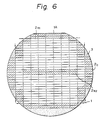
- Figure 6 is a plane view for explaining a configuration of a wafer used for a wafer scale integration device of an embodiment according to the present invention.
- references 2 R1 and 2 R2 denote real chips having an actual circuit
- 2 D denotes a dummy chip having no actual circuit.
- the actual circuit is, for example, a memory circuit and a logic circuit for actual use.
- the real chips 2 R1 which are indicated by hatching lines from the upper right side to the lower left side are the same as the real chips 2 shown in Figs 1 to 5.
- Each of the real chips includes global lines for transmitting common signals and local lines for electrically connecting each of the real chips with its neighboring real chips.
- the global lines comprise a wafer clock line WCK for transmitting a wafer clock signal and a command line CMND for transmitting a command strobe signal.
- each of the dummy chips 2 D has a plurality of metal pads made for instance of aluminium for relaying a bonding wire, each of the metal pads is at an electrically floating state. Note, each of the dummy chips 2 D does not include an actual circuit, and each of the real chips includes metal pads for receiving the power supply voltages.
- a metal film and a passivation film are not provided, but a scribe line is provided.
- the dummy chips 2 D are formed in the circumference of the wafer 1 instead of real chips 2 in the circumference of the wafer 1 shown in Fig. 1.
- the real chips are formed in the circumference of the wafer, almost all of the real chips in the circumference of the wafer do not operate by due to defects, such as short circuit of the power supply voltages.
- Figure 7 is a plane view showing cutting of the wafer 1 to a square shape suitable for mounting on the carrier. As shown in Fig. 7, all sides of the wafer 1 are cut by cutting lines, which are indicated by arrow marks in Fig. 6, in order to be mounted on the carrier.
- a plurality of dummy chips 2 D are formed in the circumference of the wafer 1. Therefore, when power lines 4 such as the Vcc and Vss lines are constituted by bonding wires, the dummy chips 2 D can be used for relay points for relaying the bonding wires, and thus the length of the long wiring portions can be shortened.
- the length of the wire becomes shorter than in the prior art. Further, after cutting the lower side which is opposite the orientation flat 1A, the metal film 3 does not remain at the left and right lower corners, and thus the length of the bonding wire becomes shorter.
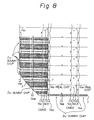
- Figure 8 is an enlarged plane view of a lower left corner portion of the wafer 1.
- reference 7 denotes a metal pad of a relay point in the dummy chip 2 D
- CMND denotes a command line
- V BB denotes a substrate voltage line.
- the power supply lines 4 of the Vss and Vcc lines are applied to the real chips 2 R1 through a plurality of dummy chips 2 D .
- the bonding wires used for the power supply lines 4 at the left and right sides are relayed by a plurality of metal pads corresponding to the dummy chips 2 D , and the relayed bonding wires are connected to the metal pads of the real chips 2 R1 .
- the power supply lines 4 are wired from the lower left and right corners through the dummy chips 2 D .
- the global lines GL are divided close to the boundary portion between the real chip 2 R2 and its neighbouring real chip.
- the power supply lines 4 are not short-circuited by the metal film 3 at the edge portions of the wafer 1.
- the metal film 3 is also not formed in the circumference of the wafer 1 and the metal film 3 is not formed in the circumference of the dummy chips 2 D , and the global lines GL and the local lines LL which extend from a space between the specific real chip to the neighbouring area of the specific real chip are not short-circuited by the metal film 3.
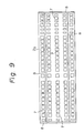
- Figure 9 is an enlarged plane view of one of the dummy chips 2 D , and reference 8 denotes a scribe line.
- the scribe line 8 is formed in the circumference of the dummy chip 2 D and the scribe line 8 does not include metal film 3 made of aluminium and the cover film made of PSG+SiN. Therefore, when cutting the wafer along the scribe line 8, slivers of aluminium do not cling to the chip, and thus reliability is not decreased. As shown in Fig. 8, in the lower side opposite the orientation flat 1A, one array of metal pads for relay points remain, this metal pad array is used for a countermeasure of the long wiring.
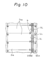
- Figure 10 is an enlarged plane view of a circular portion indicated by a broken line in Fig. 7, and reference 9 denotes a dividing portion of the global lines GL of real chips 2 R2 close to the boundary portion between the real chips 2 R2 according to an embodiment of the invention.
- a configuration as shown in Fig. 10 is very useful for bypassing defective chips and passing only operative real chips 2 R1 in serial from an input end to an output end. Namely, when one array of the chips of Y-direction cannot be used due to a short circuit of the power supply lines 4, the local lines LL cannot be passed through the defective chip array, and thus a SPIRAL path cannot be constituted by connecting all real chips 2 R1 in serial. In this case, a considerable number of real chips 2 R1 become wasted. However, in accordance with the configuration of the present invention, in this case, the local lines LL can be detoured around the defective chip array by passing through the dividing portion 9, and thus the SPIRAL path can be constituted using the remaining operative real chips 2 R1 the same as in an ordinary case.
- a plurality of dummy chips 2 D are selectively formed on an appropriate position in the circumference of a wafer 1.
- Each of the dummy chips 2 D include a plurality of metal pads 7 of a relay point formed on a surface of each of the dummy chips 2 D and a scribe line 8 which is a cutting line formed on the circumference of the dummy chip, and a metal film 3 and cover film are not provided at the scribe line 8.
- a plurality of real chips 2 R1 and 2 R2 are selectively arranged on an appropriate posistion in the center portion of the wafer.
- These real chips include an actual circuit and real pads for receiving power supply voltages, and the real chips also include global lines GL each consisting of a wafer clock line WCK and a command line CMND.
- the global lines GL are divided at a dividing portion 9 to enable passing through of local lines LL close to the boundary portion between the real chip and a neighboring chip thereof.
- the power supply lines 4 are constituted by a bonding wire for applying power supply voltages to a plurality of real chips without a potential drop.
- the power supply lines 4 are not short-circuited by the edge portions of the wafer, moreover, the global lines GL and the local lines LL do not short-circuit by the edge portions of the wafer 1. Further, when cutting the wafer 1 for mounting on the carrier, slivers of metal do not cling to the chip, and reliability is not decreased. Furthermore, it is possible for a SPIRAL path to be constituted by connecting operative chips using the local lines and not connecting defective chips.
Landscapes
- Design And Manufacture Of Integrated Circuits (AREA)
- Semiconductor Integrated Circuits (AREA)
- Semiconductor Memories (AREA)
- Wire Bonding (AREA)
Claims (6)
- Waferscaleintegrationseinrichtung mit: einem Wafer (1); einer Mehrzahl von realen Chips (2 R1, 2 R2), die selektiv in einem zentralen Bereich des Wafers (1) ausgebildet sind und jeweils eine wirkliche Schaltung und eine Mehrzahl von realen Plättchen auf der Waferoberfläche aufweisen; einer Mehrzahl von globalen Leitungen (GL) und lokalen Leitungen (LL), die auf der Waferoberfläche ausgebildet sind, wobei die globalen Leitungen (GL) gemeinsame Signale zu den realen Chips übertragen und die lokalen Leitungen (LL) jeden der realen Chips (2 R1, 2 R2) mit benachbarten realen Chips (2 R1, 2 R2) elektrisch verbinden; sowie Bonddrähten, die jedes reale Plättchen mit dem Äußeren des Wafers verbinden;
bei der die Waferscaleintegrationseinrichtung weiterhin eine Mehrzahl von Blindchips (2D) aufweist, die selektiv am Umfang des vorgeschnittenen Wafers (1) ausgebildet sind, so daß sie die realen Chips umgeben und jeder der Blindchips keine wirkliche Schaltung sondern eine Mehrzahl von Weiterleitungsplättchen (7) aufweist, die selektiv mit entsprechenden Plättchen der realen Chips verbunden sind, um die Bonddrähte zu den realen Chips weiterzuführen und die Länge der Bonddrähte von außerhalb des Wafers zu dem Wafer zu verkürzen; wobei die Peripherie jedes Blindchips von irgendeinem Metallfilm (3) freigehalten wird, der anderswo zur Bildung von Elektrodenverdrahtungen einschließlich der Weiterleitungsplättchen (7) auf die Waferoberfläche aufgebracht wird, so daß die globalen Leitungen (GL) oder die lokalen Leitungen (LL) von benachbarten realen Chips nicht kurzgeschlossen werden. - Waferscaleintegrationseinrichtung nach Anspruch 1, bei der die mit Weiterleitungsplättchen (7) verbundenen Bonddrähte zur Zuführung von Versorgungsspannungen zu den realen Chips verwendet werden.
- Waferscaleintegrationseinrichtung nach Anspruch 1, bei der jeder Blindchip (2D) eine an seinem Umfang liegende Anreiß- linie (8) zum Schneiden des Wafers (1) in quadratische Form aufweist, wobei die Anreißlinie (8) frei von dem Metallfilm (3) und einem Abdeckfilm aus Phosphorsilikat-Glas (PSG) und Siliciumnitritd (SiN) bedeckt ist, der ansonsten auf der Waferoberfläche ausgebildet sind.
- Waferscaleintegrationseinrichtung nach Anspruch 1, bei der die globalen Leitungen (GL) an einem Trennabschnitt (9) zwischen einigen (2R2) der realen Chips (2R1) unterbrochen sind, um ein Durchführen der lokalen Leitungen (LL) durch den Trennabschnitt zu ermöglichen, wenn ein defekter Chip umgangen wird.
- Waferscaleintegrationseinrichtung nach Anspruch 4, bei der die Trennabschnitte (9) zwischen einigen (2 R2) der realen Chips (2 R1, 2 R2) in Form einer Matrix im Zentrum des Wafers (1) angeordnet sind.
- Waferscaleintegrationseinrichtung nach Anspruch 4, bei der die globalen Leitungen (GL) eine Wafer-Taktleitung zur Übertragung eines Wafer-Taktsignals und eine Befehlsleitung zur Übertragung eines Befehls-Abtastsignals aufweisen.
Applications Claiming Priority (2)
| Application Number | Priority Date | Filing Date | Title |
|---|---|---|---|
| JP132589/88 | 1988-06-01 | ||
| JP63132589A JP2516403B2 (ja) | 1988-06-01 | 1988-06-01 | ウエハ・スケ―ル・メモリ |
Publications (2)
| Publication Number | Publication Date |
|---|---|
| EP0345162A1 EP0345162A1 (de) | 1989-12-06 |
| EP0345162B1 true EP0345162B1 (de) | 1994-08-31 |
Family
ID=15084877
Family Applications (1)
| Application Number | Title | Priority Date | Filing Date |
|---|---|---|---|
| EP89401508A Expired - Lifetime EP0345162B1 (de) | 1988-06-01 | 1989-06-01 | Integrierte Vorrichtung in Halbleiterscheibengrösse |
Country Status (5)
| Country | Link |
|---|---|
| US (1) | US5138419A (de) |
| EP (1) | EP0345162B1 (de) |
| JP (1) | JP2516403B2 (de) |
| KR (1) | KR920008423B1 (de) |
| DE (1) | DE68917793T2 (de) |
Families Citing this family (6)
| Publication number | Priority date | Publication date | Assignee | Title |
|---|---|---|---|---|
| JP2697150B2 (ja) | 1989-06-20 | 1998-01-14 | 富士通株式会社 | ウエーハスケールlsi |
| US5767565A (en) * | 1996-07-22 | 1998-06-16 | Alliance Semiconductor Corporation | Semiconductor devices having cooperative mode option at assembly stage and method thereof |
| US6664628B2 (en) * | 1998-07-13 | 2003-12-16 | Formfactor, Inc. | Electronic component overlapping dice of unsingulated semiconductor wafer |
| US6700142B1 (en) * | 2001-12-31 | 2004-03-02 | Hyperchip Inc. | Semiconductor wafer on which is fabricated an integrated circuit including an array of discrete functional modules |
| JP5309728B2 (ja) * | 2008-06-27 | 2013-10-09 | 富士通セミコンダクター株式会社 | レチクルデータ作成方法及びレチクルデータ作成装置 |
| US9899324B1 (en) * | 2016-11-28 | 2018-02-20 | Globalfoundries Inc. | Structure and method of conductive bus bar for resistive seed substrate plating |
Citations (1)
| Publication number | Priority date | Publication date | Assignee | Title |
|---|---|---|---|---|
| GB2178204A (en) * | 1985-07-12 | 1987-02-04 | Sinclair Res Ltd | Wafer-scale integrated circuit memory |
Family Cites Families (19)
| Publication number | Priority date | Publication date | Assignee | Title |
|---|---|---|---|---|
| JPS5568668A (en) * | 1978-11-20 | 1980-05-23 | Nippon Telegr & Teleph Corp <Ntt> | Semiconductor device |
| JPS5779655A (en) * | 1980-11-05 | 1982-05-18 | Ricoh Co Ltd | Manufacture of integrated circuit chip |
| JPS58143550A (ja) * | 1982-02-22 | 1983-08-26 | Nec Corp | 半導体装置 |
| JPS59107532A (ja) * | 1982-12-13 | 1984-06-21 | Nec Corp | 半導体装置 |
| JPS59197151A (ja) * | 1983-04-22 | 1984-11-08 | Toshiba Corp | 半導体集積回路装置 |
| FR2547112B1 (fr) * | 1983-06-03 | 1986-11-21 | Thomson Csf | Procede de realisation d'un circuit hybride et circuit hybride logique ou analogique |
| JPS6020526A (ja) * | 1983-07-15 | 1985-02-01 | Hitachi Ltd | 半導体装置 |
| JPS6049648A (ja) * | 1983-08-30 | 1985-03-18 | Sumitomo Electric Ind Ltd | マスタスライスic |
| US4703436A (en) * | 1984-02-01 | 1987-10-27 | Inova Microelectronics Corporation | Wafer level integration technique |
| JPH0714002B2 (ja) * | 1984-05-15 | 1995-02-15 | セイコーエプソン株式会社 | チップへの信号供給方法 |
| JPS6130044A (ja) * | 1984-07-20 | 1986-02-12 | Nippon Denso Co Ltd | 半導体チツプの検査方法 |
| JPS6187349A (ja) * | 1984-10-04 | 1986-05-02 | Nippon Denso Co Ltd | 半導体ウエハ |
| JPS61214559A (ja) * | 1985-03-20 | 1986-09-24 | Hitachi Ltd | 半導体集積回路装置 |
| JPS62179755A (ja) * | 1986-02-03 | 1987-08-06 | Mitsubishi Electric Corp | テスト回路内蔵半導体集積回路 |
| JPS62219957A (ja) * | 1986-03-20 | 1987-09-28 | Fujitsu Ltd | Lsi素子内の入出力回路 |
| JPS62224056A (ja) * | 1986-03-26 | 1987-10-02 | Hitachi Ltd | 半導体装置 |
| JPS62238637A (ja) * | 1986-04-09 | 1987-10-19 | Nec Kansai Ltd | パタ−ン位置合わせ方法 |
| JPS63114246A (ja) * | 1986-10-31 | 1988-05-19 | Mitsubishi Electric Corp | 半導体装置 |
| JPH03106029A (ja) * | 1989-09-20 | 1991-05-02 | Fujitsu Ltd | ウエハ・スケール・ic |
-
1988
- 1988-06-01 JP JP63132589A patent/JP2516403B2/ja not_active Expired - Fee Related
-
1989
- 1989-06-01 DE DE68917793T patent/DE68917793T2/de not_active Expired - Fee Related
- 1989-06-01 EP EP89401508A patent/EP0345162B1/de not_active Expired - Lifetime
- 1989-06-01 KR KR1019890007512A patent/KR920008423B1/ko not_active Expired
-
1991
- 1991-05-28 US US07/707,936 patent/US5138419A/en not_active Expired - Lifetime
Patent Citations (1)
| Publication number | Priority date | Publication date | Assignee | Title |
|---|---|---|---|---|
| GB2178204A (en) * | 1985-07-12 | 1987-02-04 | Sinclair Res Ltd | Wafer-scale integrated circuit memory |
Also Published As
| Publication number | Publication date |
|---|---|
| US5138419A (en) | 1992-08-11 |
| EP0345162A1 (de) | 1989-12-06 |
| JPH01303750A (ja) | 1989-12-07 |
| DE68917793T2 (de) | 1995-01-05 |
| DE68917793D1 (de) | 1994-10-06 |
| JP2516403B2 (ja) | 1996-07-24 |
| KR910001967A (ko) | 1991-01-31 |
| KR920008423B1 (ko) | 1992-09-28 |
Similar Documents
| Publication | Publication Date | Title |
|---|---|---|
| US12021035B2 (en) | Interconnecting dies by stitch routing | |
| US4254445A (en) | Discretionary fly wire chip interconnection | |
| EP0070861B1 (de) | Integrierte halbleiterscheibe sowie methode zur prüfung von auf dieser scheibe enthaltenen schaltungen | |
| JPH0727968B2 (ja) | 半導体集積回路装置 | |
| JPS58127357A (ja) | 集積回路チツプ・モジユ−ル | |
| US10295588B2 (en) | Wafer testing without direct probing | |
| US6114903A (en) | Layout architecture for core I/O buffer | |
| EP0361825A2 (de) | Halbleiterchip und Verfahren zu seiner Herstellung | |
| US4988636A (en) | Method of making bit stack compatible input/output circuits | |
| EP0345162B1 (de) | Integrierte Vorrichtung in Halbleiterscheibengrösse | |
| US5616931A (en) | Semiconductor device | |
| US6933611B2 (en) | Selective solder bump application | |
| EP0069762B1 (de) | Ein universelles substrat zur wechselseitigen elektrischen verbindung von chips | |
| EP0418777B1 (de) | Halbleiteranordnung auf Scheibenskala | |
| JP3192220B2 (ja) | 回路モジュール冗長性アーキテクチャ | |
| EP0418802B1 (de) | Leiterstruktur mit grösstintegrierter Schaltung auf einem Wafer | |
| WO1989012320A1 (en) | Wafer scale integrated circuits | |
| JP2716399B2 (ja) | 半導体集積回路装置 | |
| JPH01307243A (ja) | 半導体集積回路装置 | |
| KR20000008137A (ko) | 반도체 장치의 테그 패턴 형성방법 | |
| JPS58202547A (ja) | 集積回路装置 | |
| KR940004444B1 (ko) | 웨이퍼 스케일(wafer-scale) 반도체 집적회로장치 및 웨이퍼 스케일 반도체 집적회로장치의 칩간에 배열되는 접속배선의 형성방법 | |
| KR20050011393A (ko) | 다기능 패드를 갖는 반도체 메모리 장치 및 다기능 패드배치방법 |
Legal Events
| Date | Code | Title | Description |
|---|---|---|---|
| PUAI | Public reference made under article 153(3) epc to a published international application that has entered the european phase |
Free format text: ORIGINAL CODE: 0009012 |
|
| AK | Designated contracting states |
Kind code of ref document: A1 Designated state(s): DE FR GB |
|
| 17P | Request for examination filed |
Effective date: 19900524 |
|
| 17Q | First examination report despatched |
Effective date: 19920204 |
|
| GRAA | (expected) grant |
Free format text: ORIGINAL CODE: 0009210 |
|
| AK | Designated contracting states |
Kind code of ref document: B1 Designated state(s): DE FR GB |
|
| PG25 | Lapsed in a contracting state [announced via postgrant information from national office to epo] |
Ref country code: FR Effective date: 19940831 |
|
| REF | Corresponds to: |
Ref document number: 68917793 Country of ref document: DE Date of ref document: 19941006 |
|
| EN | Fr: translation not filed | ||
| PLBE | No opposition filed within time limit |
Free format text: ORIGINAL CODE: 0009261 |
|
| STAA | Information on the status of an ep patent application or granted ep patent |
Free format text: STATUS: NO OPPOSITION FILED WITHIN TIME LIMIT |
|
| 26N | No opposition filed | ||
| REG | Reference to a national code |
Ref country code: GB Ref legal event code: IF02 |
|
| PGFP | Annual fee paid to national office [announced via postgrant information from national office to epo] |
Ref country code: DE Payment date: 20060525 Year of fee payment: 18 |
|
| PGFP | Annual fee paid to national office [announced via postgrant information from national office to epo] |
Ref country code: GB Payment date: 20060531 Year of fee payment: 18 |
|
| GBPC | Gb: european patent ceased through non-payment of renewal fee |
Effective date: 20070601 |
|
| PG25 | Lapsed in a contracting state [announced via postgrant information from national office to epo] |
Ref country code: DE Free format text: LAPSE BECAUSE OF NON-PAYMENT OF DUE FEES Effective date: 20080101 |
|
| PG25 | Lapsed in a contracting state [announced via postgrant information from national office to epo] |
Ref country code: GB Free format text: LAPSE BECAUSE OF NON-PAYMENT OF DUE FEES Effective date: 20070601 |