EP0345507A2 - Nicht-abstimmbares monolithisches Keramikfilter - Google Patents
Nicht-abstimmbares monolithisches Keramikfilter Download PDFInfo
- Publication number
- EP0345507A2 EP0345507A2 EP89109027A EP89109027A EP0345507A2 EP 0345507 A2 EP0345507 A2 EP 0345507A2 EP 89109027 A EP89109027 A EP 89109027A EP 89109027 A EP89109027 A EP 89109027A EP 0345507 A2 EP0345507 A2 EP 0345507A2
- Authority
- EP
- European Patent Office
- Prior art keywords
- dielectric
- dielectric means
- frequency related
- filter
- related characteristic
- Prior art date
- Legal status (The legal status is an assumption and is not a legal conclusion. Google has not performed a legal analysis and makes no representation as to the accuracy of the status listed.)
- Granted
Links
Images
Classifications
-
- H—ELECTRICITY
- H03—ELECTRONIC CIRCUITRY
- H03H—IMPEDANCE NETWORKS, e.g. RESONANT CIRCUITS; RESONATORS
- H03H1/00—Constructional details of impedance networks whose electrical mode of operation is not specified or applicable to more than one type of network
-
- H—ELECTRICITY
- H01—ELECTRIC ELEMENTS
- H01P—WAVEGUIDES; RESONATORS, LINES, OR OTHER DEVICES OF THE WAVEGUIDE TYPE
- H01P1/00—Auxiliary devices
- H01P1/20—Frequency-selective devices, e.g. filters
- H01P1/201—Filters for transverse electromagnetic waves
- H01P1/205—Comb or interdigital filters; Cascaded coaxial cavities
- H01P1/2056—Comb filters or interdigital filters with metallised resonator holes in a dielectric block
-
- H—ELECTRICITY
- H01—ELECTRIC ELEMENTS
- H01P—WAVEGUIDES; RESONATORS, LINES, OR OTHER DEVICES OF THE WAVEGUIDE TYPE
- H01P1/00—Auxiliary devices
- H01P1/20—Frequency-selective devices, e.g. filters
- H01P1/201—Filters for transverse electromagnetic waves
- H01P1/205—Comb or interdigital filters; Cascaded coaxial cavities
Definitions
- the present invention relates generally to radio-frequency (RF) signal filters, and, more particularly, to the practice of tuning ceramic RF signal filters.
- Conventional multi-resonator ceramic filters include a plurality of resonators that are typically foreshortened short-circuited quarter wavelength coaxial or helical transmission lines.
- the resonators are arranged in a conductive enclosure and may be coupled one to another by apertures in their common walls.
- Each resonator is commonly tuned to the desired response characteristics in one of two ways.
- tuning such resonators is by employing a tuning screw which inserts into a hole extending through the middle of the resonator.
- the tuning screw is bulky, it requires mechanical locking elements which can offset the desired coupling between resonators, and, due to the adjustability of the screw before it is locked, it renders these filters susceptible to becoming detuned.
- Another way of tuning each resonator is by plating one surface of the ceramic filter at each resonator with conductive plating material. Typically, the surface is plated between the hole in the middle of the resonator and a side wall coupled to the conductive enclosure. This plating is then etched (abraded) away for each resonator in the filter until the desired response characteristics are obtained.
- This approach is disadvantageous in that it is extremely labor intensive. Plating at each resonator must be repeatedly etched and tested for the desired response characteristics. If too much plating is removed, the filter must be replated or discarded. Moreover, etching the plating often results in etching away some of the ceramic material of the resonator which degrades the coupling consistency between the resonators.
- the arrangement disclosed in this specification has particular use for filtering signals in a radio frequency (RF) communication system. More particularly, the arrangement disclosed herein is directed to the manufacture of ceramic filters, their implementation as a duplexer in a radio transceiver.
- RF radio frequency
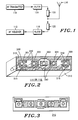
- Fig. 1 illustrates such a transceiver.
- the transceiver includes a conventional RF transmitter 110, and a conventional RF receiver 112.
- a novel ceramic filter 114 is used to couple a transmit signal from the RF transmitter 110 to an antenna 116.
- a similar novel ceramic filter 118 is employed between the antenna 116 and the RF receiver 112 to couple a received RF signal from the antenna 116 to the RF receiver 112.
- the filters 114 and 118 function as a duplexer to intercouple the antenna 116 to the transceiver.
- Transmission lines 120 and 122 are respectively disposed between the ceramic filters 114 and 118 and the antenna 116 for proper electrical coupling.
- the passband of the filter 114 is centered about the frequency of the transmit signal from RF transmitter 110, while at the same time greatly attenuating the frequency of the received RF signal.
- the length of transmission line 120 is selected to maximize its impedance at the frequency of the received signal.
- the passband of the filter 118 is centered about the frequency of the received RF signal, while at the same time greatly attenuating the transmit signal.
- the length of transmission line 122 is selected to maximize its impedance at the transmit signal frequency.
- the filters 114 and 118 with elements 120 and 122 can be combined onto a single dielectric block.
- the filter 114 or 118 is shown in detail, according to the present invention.
- the filter 114 or 118 includes a block 210 which is comprised of a dielectric material that is selectively plated with a conductive material.
- the block 210 includes input and output electrodes 214 and 216 plated thereon for receiving an input RF signal and for passing a filtered RF signal, respectively.
- RF signals can be coupled to the electrodes 214 and 216 of the filter 114 or 118 by conventional circuits such as those discussed in U.S. Pat. No. 4,431,977, Sokola et al., assigned to the same assignee and incorporated herein by reference.
- the plating on block 210 is electrically conductive, preferably copper, silver or an alloy thereof. Such plating preferably covers all surfaces of the block 210 with the exception of the top surface 212, the plating of which is discussed below. Of course, other conductive plating arrangements can be utilized. See, for example, those discussed in "Ceramic Bandpass Filter", U.S. Pat. No. 4,431,977, Sokola et al., assignee to the present assignee and incorporated herein by reference.
- Block 210 includes five holes 201-205, each of which extends from the top surface to the bottom surface thereof.
- the surfaces defining holes 201-205 are likewise plated with an electrically conductive material.
- Each of the plated holes 201-205 is essentially a transmission line resonator comprised of a short-circuited coaxial transmission line having a length selected for desired filter response characteristics.
- block 210 is shown with five plated holes 201-207, any number of plated holes can be utilized depending on the filter response characteristics desired. For additional description of the holes 201-205, reference may be made to U.S. Pat. No. 4,431,977, Sokola et al., supra.
- ceramic waveguide filters sometimes include resonating section(s) without holes through the dielectric block. See, for example, U.S. Pat. No. 4,691,179, Blum et al., assigned to the same assignee and incorportated herein by reference.
- Coupling between the transmission line resonators, provided by the plated holes 201-205, in Fig. 2 is accomplished through the dielectric material and is coursely adjusted by varying the effective width of the dielectric material and the distance between adjacent transmission line resonators.
- the effective width of the dielectric material between adjacent holes 201-205 can be adjusted in any suitable regular or irregular manner; for example, by the use of slots, cylindrical holes, square or rectangular holes, or irregular shaped holes.
- Fine adjustments are made according to the predesigned artwork plating as discussed below.
- plated or unplated holes located between the transmission line resonators, provided by holes 201-205, can also be utilized for adjusting the coupling.
- a top surface 212 of the block 210 is selectively plated with a similar electrically conductive material (plating) 240, indicated by shaded areas.
- the unplated areas of the top surface 212, gaps between the plated areas, are indicated by the unshaded areas.
- the plating 240 on the top surface of block 210 of Fig. 2 is disposed on the block 210 by using a predesigned artwork mask 310 (Fig. 3), in accordance with the present invention.
- the unique mask design is based upon a selected frequency related characteristic of the base dielectric block.
- the selected frequency related characteristic includes the quarter wave length frequency of the base dielectric block.
- the height and the dielectric constant of the base dielectric block can be used.
- the base dielectric block can be constructed of a suitable dielectric material that has low loss, a high dielectric constant and a low temperature coefficient of the dielectric constant.
- the base dielectric block of block 210 is comprised of a ceramic compound including barium oxide, titanium oxide and zirconium oxide, the electrical characteristics of which are described in more detail in an article by G. H. Jonker and W. Kwestroo, entitled “The Ternary Systems BzO-TiO2-SnO2 and BaO-TiO2-ZrO2", published in the Journal of the American Ceramic Society, volume 41, number 10, at pages 390-394, October 1958.
- the compound in Table VI having the composition 18.5 mole % BaO, 77.0 mole % TiO2 and 4.5 mole % ZrO2 and having a dielectric constant of 40 is well suited for use in the ceramic filter of the present invention.
- Such dielectric material is preferably employed as a batch, useful for developing a large number of base dielectric blocks.
- One batch of such dielectric material when appropriately used, will provide an equal distribution of the elements making up the compound. An equal distribution will ensure almost exact frequency related characteristics throughout the base dielectric blocks produced therefrom. For example, variance of the quarter wavelength resonant frequency is negligible (measured at less than 0.4% in one application) between the blocks produced from the same batch. However, such a characteristic may be measured on various samples from the batch to ensure consistency.
- the selected frequency related characteristic is measured to determine the representative frequency related characteristic for the batch or a substantial portion thereof.
- plating artwork useful for selectively plating the conductive material to the top surface of the blocks is designed and then applied to the base dielectric block to provide a complete filter with customized filter characteristics.
- the artwork is developed using conventional computer program modeling and model-to-circuit translations, such as the program entitled "Super-Compact", available from Compact Software, Inc.
- the manner in which the plating artwork is used to apply the plating to the base dielectric block can be accomplished using conventional means.
- an adequate technique uses a dry film imaging transfer system such as Riston R by Du Pont Electronics, Inc., subsidiary of E.I. Du Pont De Nemours & Co. (Inc.).
- Variance of the frequency related characteristic between batches can be accommodated by designing several artwork masks to represent needed shifts of the desired center frequency of the filter. For example, consider a quarter wave length base dielectric block frequency of 1 GHz. and a desired filter center frequency of 836.5 MHz. The artwork will be designed to shift the quarter wave length frequency down to 836.5 MHz. However, various batches may result in a quarter wave length base dielectric block frequencies which vary from 0.990 GHz. to 1.010 GHz. (20 MHz. variance). By designing seven artwork masks, each may be designed to shift a quarter wave length base dielectric block frequency as below: Artwork Shift from Shift to 1 1.010 GHz. 836.5 MHz. 2 1.007 GHz. 836.5 MHz.
- a 20 MHz. variance from one batch to the next may be compensated to within 3 Mhz. accuracy by measuring the quarter wavelength frequency characteristic and then selecting the appropriate artwork mask with which to apply the block plating.
- the plating artwork is developed to shift the resonant frequency of the block down to the specified center resonant frequency for the filter design.
- This processing technique provides significant advantages over the prior art previously discussed. For example, a twelve block study of screen printed and tuned filters included frequency, gap and coupling coefficient measurements. The twelve filters met the desired insertion loss and attentuation specifications as well or better than by abrasive conventional tuning techniques.
Landscapes
- Physics & Mathematics (AREA)
- Electromagnetism (AREA)
- Control Of Motors That Do Not Use Commutators (AREA)
- Filtering Materials (AREA)
- Thermistors And Varistors (AREA)
- Fixed Capacitors And Capacitor Manufacturing Machines (AREA)
- Inorganic Insulating Materials (AREA)
- Measurement Of Resistance Or Impedance (AREA)
Applications Claiming Priority (2)
| Application Number | Priority Date | Filing Date | Title |
|---|---|---|---|
| US20262388A | 1988-06-06 | 1988-06-06 | |
| US202623 | 1988-06-06 |
Publications (3)
| Publication Number | Publication Date |
|---|---|
| EP0345507A2 true EP0345507A2 (de) | 1989-12-13 |
| EP0345507A3 EP0345507A3 (en) | 1990-09-12 |
| EP0345507B1 EP0345507B1 (de) | 1994-07-20 |
Family
ID=22750644
Family Applications (1)
| Application Number | Title | Priority Date | Filing Date |
|---|---|---|---|
| EP89109027A Expired - Lifetime EP0345507B1 (de) | 1988-06-06 | 1989-05-19 | Nicht-abstimmbares monolithisches Keramikfilter |
Country Status (9)
| Country | Link |
|---|---|
| EP (1) | EP0345507B1 (de) |
| JP (1) | JPH06103802B2 (de) |
| KR (1) | KR930002634B1 (de) |
| AT (1) | ATE108951T1 (de) |
| CA (1) | CA1311535C (de) |
| DE (1) | DE68916865T2 (de) |
| FI (1) | FI96457C (de) |
| IE (1) | IE65457B1 (de) |
| MX (1) | MX169825B (de) |
Cited By (1)
| Publication number | Priority date | Publication date | Assignee | Title |
|---|---|---|---|---|
| EP1009059A1 (de) * | 1998-12-10 | 2000-06-14 | Ngk Spark Plug Co., Ltd | Dielektrisches Filter mit regelbarer Frequenzbandbreite |
Family Cites Families (4)
| Publication number | Priority date | Publication date | Assignee | Title |
|---|---|---|---|---|
| US4266206A (en) * | 1978-08-31 | 1981-05-05 | Motorola, Inc. | Stripline filter device |
| JPS6285002U (de) * | 1985-11-18 | 1987-05-30 | ||
| US4716391A (en) * | 1986-07-25 | 1987-12-29 | Motorola, Inc. | Multiple resonator component-mountable filter |
| JPS6342201A (ja) * | 1986-08-07 | 1988-02-23 | Alps Electric Co Ltd | マイクロ波分波器 |
-
1989
- 1989-05-08 CA CA000599011A patent/CA1311535C/en not_active Expired - Lifetime
- 1989-05-19 DE DE68916865T patent/DE68916865T2/de not_active Expired - Lifetime
- 1989-05-19 AT AT89109027T patent/ATE108951T1/de not_active IP Right Cessation
- 1989-05-19 EP EP89109027A patent/EP0345507B1/de not_active Expired - Lifetime
- 1989-05-23 FI FI892501A patent/FI96457C/fi not_active IP Right Cessation
- 1989-05-24 MX MX016175A patent/MX169825B/es unknown
- 1989-05-30 JP JP1137314A patent/JPH06103802B2/ja not_active Expired - Lifetime
- 1989-06-02 KR KR1019890007574A patent/KR930002634B1/ko not_active Expired - Fee Related
- 1989-06-12 IE IE174689A patent/IE65457B1/en not_active IP Right Cessation
Cited By (2)
| Publication number | Priority date | Publication date | Assignee | Title |
|---|---|---|---|---|
| EP1009059A1 (de) * | 1998-12-10 | 2000-06-14 | Ngk Spark Plug Co., Ltd | Dielektrisches Filter mit regelbarer Frequenzbandbreite |
| US6304159B1 (en) | 1998-12-10 | 2001-10-16 | Ngk Spark Plug Co., Ltd. | Dielectric filter with adjustable frequency bandwidth |
Also Published As
| Publication number | Publication date |
|---|---|
| JPH06103802B2 (ja) | 1994-12-14 |
| EP0345507B1 (de) | 1994-07-20 |
| ATE108951T1 (de) | 1994-08-15 |
| KR930002634B1 (ko) | 1993-04-06 |
| DE68916865T2 (de) | 1995-01-26 |
| FI892501A0 (fi) | 1989-05-23 |
| CA1311535C (en) | 1992-12-15 |
| DE68916865D1 (de) | 1994-08-25 |
| FI96457B (fi) | 1996-03-15 |
| IE891746L (en) | 1989-12-06 |
| EP0345507A3 (en) | 1990-09-12 |
| FI96457C (fi) | 1996-06-25 |
| FI892501L (fi) | 1989-12-07 |
| IE65457B1 (en) | 1995-11-01 |
| MX169825B (es) | 1993-07-27 |
| KR900001118A (ko) | 1990-01-31 |
| JPH0227801A (ja) | 1990-01-30 |
Similar Documents
| Publication | Publication Date | Title |
|---|---|---|
| US4965537A (en) | Tuneless monolithic ceramic filter manufactured by using an art-work mask process | |
| US5004992A (en) | Multi-resonator ceramic filter and method for tuning and adjusting the resonators thereof | |
| EP0100350B1 (de) | Keramischer bandfilter | |
| US5543764A (en) | Filter having an electromagnetically tunable transmission zero | |
| US4823098A (en) | Monolithic ceramic filter with bandstop function | |
| US4963843A (en) | Stripline filter with combline resonators | |
| US4742562A (en) | Single-block dual-passband ceramic filter useable with a transceiver | |
| US4418324A (en) | Implementation of a tunable transmission zero on transmission line filters | |
| EP0815612B1 (de) | Dielektrischer resonatorfilter | |
| KR960007806B1 (ko) | 전자 필터 장치 및 그의 동조 방법 | |
| US3840828A (en) | Temperature-stable dielectric resonator filters for stripline | |
| EP0734088A1 (de) | Dielektrischer Resonator und dielektrische Resonatorvorrichtung damit | |
| JP2005117675A (ja) | Rfセラミックフィルターの製造方法 | |
| US2704830A (en) | Tuning means for dielectric filled cavity resonators | |
| US4462098A (en) | Radio frequency signal combining/sorting apparatus | |
| WO1992017914A1 (en) | Half wave resonator dielectric filter construction having self-shielding top and bottom surfaces | |
| US4630012A (en) | Ring shaped dielectric resonator with adjustable tuning screw extending upwardly into ring opening | |
| EP0415558A2 (de) | Bandpassfilter und Verfahren zum Abgleichen von dessen Charakteristika | |
| JPS59114902A (ja) | 誘電体フイルタ | |
| EP0345507B1 (de) | Nicht-abstimmbares monolithisches Keramikfilter | |
| US4745379A (en) | Launcher-less and lumped capacitor-less ceramic comb-line filters | |
| US5075651A (en) | VHF wide-bandwidth low impedance monolithic crystal filter having bridged electrodes | |
| JPS6150522B2 (de) | ||
| EP1009059A1 (de) | Dielektrisches Filter mit regelbarer Frequenzbandbreite | |
| HK87090A (en) | Ceramic bandpass filter |
Legal Events
| Date | Code | Title | Description |
|---|---|---|---|
| PUAI | Public reference made under article 153(3) epc to a published international application that has entered the european phase |
Free format text: ORIGINAL CODE: 0009012 |
|
| AK | Designated contracting states |
Kind code of ref document: A2 Designated state(s): AT BE CH DE ES FR GB GR IT LI LU NL SE |
|
| PUAL | Search report despatched |
Free format text: ORIGINAL CODE: 0009013 |
|
| AK | Designated contracting states |
Kind code of ref document: A3 Designated state(s): AT BE CH DE ES FR GB GR IT LI LU NL SE |
|
| 17P | Request for examination filed |
Effective date: 19910222 |
|
| 17Q | First examination report despatched |
Effective date: 19930525 |
|
| GRAA | (expected) grant |
Free format text: ORIGINAL CODE: 0009210 |
|
| ITF | It: translation for a ep patent filed | ||
| AK | Designated contracting states |
Kind code of ref document: B1 Designated state(s): AT BE CH DE ES FR GB GR IT LI LU NL SE |
|
| PG25 | Lapsed in a contracting state [announced via postgrant information from national office to epo] |
Ref country code: NL Effective date: 19940720 Ref country code: GR Free format text: LAPSE BECAUSE OF FAILURE TO SUBMIT A TRANSLATION OF THE DESCRIPTION OR TO PAY THE FEE WITHIN THE PRESCRIBED TIME-LIMIT Effective date: 19940720 Ref country code: ES Free format text: THE PATENT HAS BEEN ANNULLED BY A DECISION OF A NATIONAL AUTHORITY Effective date: 19940720 Ref country code: BE Effective date: 19940720 Ref country code: CH Effective date: 19940720 Ref country code: AT Effective date: 19940720 Ref country code: LI Effective date: 19940720 |
|
| REF | Corresponds to: |
Ref document number: 108951 Country of ref document: AT Date of ref document: 19940815 Kind code of ref document: T |
|
| REF | Corresponds to: |
Ref document number: 68916865 Country of ref document: DE Date of ref document: 19940825 |
|
| PG25 | Lapsed in a contracting state [announced via postgrant information from national office to epo] |
Ref country code: SE Effective date: 19941020 |
|
| REG | Reference to a national code |
Ref country code: CH Ref legal event code: PL |
|
| ET | Fr: translation filed | ||
| NLV1 | Nl: lapsed or annulled due to failure to fulfill the requirements of art. 29p and 29m of the patents act | ||
| PLBE | No opposition filed within time limit |
Free format text: ORIGINAL CODE: 0009261 |
|
| STAA | Information on the status of an ep patent application or granted ep patent |
Free format text: STATUS: NO OPPOSITION FILED WITHIN TIME LIMIT |
|
| PG25 | Lapsed in a contracting state [announced via postgrant information from national office to epo] |
Ref country code: LU Free format text: LAPSE BECAUSE OF NON-PAYMENT OF DUE FEES Effective date: 19950531 |
|
| 26N | No opposition filed | ||
| REG | Reference to a national code |
Ref country code: GB Ref legal event code: IF02 |
|
| PG25 | Lapsed in a contracting state [announced via postgrant information from national office to epo] |
Ref country code: IT Free format text: LAPSE BECAUSE OF NON-PAYMENT OF DUE FEES;WARNING: LAPSES OF ITALIAN PATENTS WITH EFFECTIVE DATE BEFORE 2007 MAY HAVE OCCURRED AT ANY TIME BEFORE 2007. THE CORRECT EFFECTIVE DATE MAY BE DIFFERENT FROM THE ONE RECORDED. Effective date: 20050519 |
|
| PGFP | Annual fee paid to national office [announced via postgrant information from national office to epo] |
Ref country code: DE Payment date: 20080630 Year of fee payment: 20 |
|
| PGFP | Annual fee paid to national office [announced via postgrant information from national office to epo] |
Ref country code: GB Payment date: 20080529 Year of fee payment: 20 |
|
| REG | Reference to a national code |
Ref country code: GB Ref legal event code: PE20 Expiry date: 20090518 |
|
| PG25 | Lapsed in a contracting state [announced via postgrant information from national office to epo] |
Ref country code: GB Free format text: LAPSE BECAUSE OF EXPIRATION OF PROTECTION Effective date: 20090518 |
|
| PGFP | Annual fee paid to national office [announced via postgrant information from national office to epo] |
Ref country code: FR Payment date: 20080519 Year of fee payment: 20 |