EP0346061A2 - Integrierte Schaltungsanordnung mit einer verbesserten Packungsstruktur - Google Patents
Integrierte Schaltungsanordnung mit einer verbesserten Packungsstruktur Download PDFInfo
- Publication number
- EP0346061A2 EP0346061A2 EP89305678A EP89305678A EP0346061A2 EP 0346061 A2 EP0346061 A2 EP 0346061A2 EP 89305678 A EP89305678 A EP 89305678A EP 89305678 A EP89305678 A EP 89305678A EP 0346061 A2 EP0346061 A2 EP 0346061A2
- Authority
- EP
- European Patent Office
- Prior art keywords
- integrated circuit
- terminals
- group
- external connection
- circuit device
- Prior art date
- Legal status (The legal status is an assumption and is not a legal conclusion. Google has not performed a legal analysis and makes no representation as to the accuracy of the status listed.)
- Withdrawn
Links
Images



Classifications
-
- H—ELECTRICITY
- H10—SEMICONDUCTOR DEVICES; ELECTRIC SOLID-STATE DEVICES NOT OTHERWISE PROVIDED FOR
- H10W—GENERIC PACKAGES, INTERCONNECTIONS, CONNECTORS OR OTHER CONSTRUCTIONAL DETAILS OF DEVICES COVERED BY CLASS H10
- H10W70/00—Package substrates; Interposers; Redistribution layers [RDL]
- H10W70/60—Insulating or insulated package substrates; Interposers; Redistribution layers
- H10W70/67—Insulating or insulated package substrates; Interposers; Redistribution layers characterised by their insulating layers or insulating parts
- H10W70/68—Shapes or dispositions thereof
- H10W70/685—Shapes or dispositions thereof comprising multiple insulating layers
-
- H—ELECTRICITY
- H10—SEMICONDUCTOR DEVICES; ELECTRIC SOLID-STATE DEVICES NOT OTHERWISE PROVIDED FOR
- H10W—GENERIC PACKAGES, INTERCONNECTIONS, CONNECTORS OR OTHER CONSTRUCTIONAL DETAILS OF DEVICES COVERED BY CLASS H10
- H10W76/00—Containers; Fillings or auxiliary members therefor; Seals
- H10W76/10—Containers or parts thereof
- H10W76/12—Containers or parts thereof characterised by their shape
- H10W76/15—Containers comprising an insulating or insulated base
- H10W76/157—Containers comprising an insulating or insulated base having interconnections parallel to the insulating or insulated base
-
- H—ELECTRICITY
- H10—SEMICONDUCTOR DEVICES; ELECTRIC SOLID-STATE DEVICES NOT OTHERWISE PROVIDED FOR
- H10W—GENERIC PACKAGES, INTERCONNECTIONS, CONNECTORS OR OTHER CONSTRUCTIONAL DETAILS OF DEVICES COVERED BY CLASS H10
- H10W90/00—Package configurations
- H10W90/401—Package configurations characterised by multiple insulating or insulated package substrates, interposers or RDLs
-
- H—ELECTRICITY
- H10—SEMICONDUCTOR DEVICES; ELECTRIC SOLID-STATE DEVICES NOT OTHERWISE PROVIDED FOR
- H10W—GENERIC PACKAGES, INTERCONNECTIONS, CONNECTORS OR OTHER CONSTRUCTIONAL DETAILS OF DEVICES COVERED BY CLASS H10
- H10W70/00—Package substrates; Interposers; Redistribution layers [RDL]
- H10W70/60—Insulating or insulated package substrates; Interposers; Redistribution layers
- H10W70/62—Insulating or insulated package substrates; Interposers; Redistribution layers characterised by their interconnections
- H10W70/65—Shapes or dispositions of interconnections
- H10W70/654—Top-view layouts
- H10W70/655—Fan-out layouts
-
- H—ELECTRICITY
- H10—SEMICONDUCTOR DEVICES; ELECTRIC SOLID-STATE DEVICES NOT OTHERWISE PROVIDED FOR
- H10W—GENERIC PACKAGES, INTERCONNECTIONS, CONNECTORS OR OTHER CONSTRUCTIONAL DETAILS OF DEVICES COVERED BY CLASS H10
- H10W70/00—Package substrates; Interposers; Redistribution layers [RDL]
- H10W70/60—Insulating or insulated package substrates; Interposers; Redistribution layers
- H10W70/67—Insulating or insulated package substrates; Interposers; Redistribution layers characterised by their insulating layers or insulating parts
- H10W70/68—Shapes or dispositions thereof
- H10W70/682—Shapes or dispositions thereof comprising holes having chips therein
-
- H—ELECTRICITY
- H10—SEMICONDUCTOR DEVICES; ELECTRIC SOLID-STATE DEVICES NOT OTHERWISE PROVIDED FOR
- H10W—GENERIC PACKAGES, INTERCONNECTIONS, CONNECTORS OR OTHER CONSTRUCTIONAL DETAILS OF DEVICES COVERED BY CLASS H10
- H10W90/00—Package configurations
- H10W90/701—Package configurations characterised by the relative positions of pads or connectors relative to package parts
- H10W90/751—Package configurations characterised by the relative positions of pads or connectors relative to package parts of bond wires
- H10W90/754—Package configurations characterised by the relative positions of pads or connectors relative to package parts of bond wires between a chip and a stacked insulating package substrate, interposer or RDL
Definitions
- the present invention generally relates to an integrated circuit device having an improved package structure, and particularly to an improvement of a package, which mounts an integrated circuit chip and is used at the time of developing and verifying a program written into the integrated circuit chip or confirming operation of a system having the integrated circuit device.
- the present invention is suitable for developing and evaluating an application specific integrated circuit digital signal processor (ASIC DSP), microprocessor or the like.
- ASIC DSP application specific integrated circuit digital signal processor
- an integrated circuit chip such as a digital signal processor and a microprocessor has a memory, which is left open to the programming by users so as to construct a desired circuit.
- an erasable programmable read only memory hereinafter simply referred to as an EPROM
- an application specific processor is used as a memory provided in an application specific processor.
- a piggy back package is a well-known package, and has a socket, which is mounted on top of a package body.
- the socket has first terminals coupled to terminals provided in the package body, and second terminals to be coupled to a plug having a terminal arrangement identical to that of the second terminals.
- An integrated circuit chip accommodated in the package body is coupled to a tool such as a debugger and an emulator through the socket, plug and cable. In this state, it is possible to monitor the state of internal memories registers appearing before and after executing an instruction, for example.
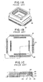
- FIGS.1A, 1B and 1C illustrate a conventional piggy back type package.
- the illustrated package includes a package body 21, and a leadless chip carrier type socket 31, which is mounted on top of the package body 21.
- the package body 21 is made up of a plurality of stacked seramics layers.
- a semiconductor chip 26 in which an integrated circuit is formed, is provided in a chip mounting layer 22, which is one of the stacked ceramics layers.
- pin receiving members 28 which is to engage with socket pin terminals 32 provided in the socket 31.
- the socket pin terminals 32 and the corresponding pin receiving members 28 are mutually connected by soldering.
- the package body 21 includes conductive patterns 42, which are served as wiring lines or internal connection lines and are connected to the related external connection terminals 25 and the pin receiving members 28.
- the internal connection lines 42 extend up to a surface of a wire bonding layer 23. Bonding wires 27 connect the internal connection lines 42 and related bonding pads formed on the surface of the wire bonding layer 23.
- FIG.2 illustrates another conventional piggy back type package.
- the illustrated package includes a package body 71 having a plurality of stacked ceramics layers into which a silicon semiconductor chip is accommodated.
- the package body 71 is provided with a plurality of external connection terminals 72 and pin receiving members, with which pin terminals of a socket 81 engage.
- Each of the external connection terminals 72 is in the form of a pin, which is inserted into a corresponding through hole formed in a printed circuit board.
- the above-mentioned packages may be provided with some improvements.
- an improvement is that the package bodies 21 and 71 are miniaturized in order to enhance the element mounting density.
- Another improvement is to employ a large size of socket to thereby attain an increased number of terminals used for evaluating the chip.
- Still another improvement is that the outer diameter of the package body 21, 71 is set equal to that of the socket 31, 81 in order to satisfy both the miniaturization of the package body and increase of the size of the socket.
- the package illustrated in FIGS.1A through 1C is designed to visually investigate the contact state of the socket pin terminals 32 and the pin receiving members 28 through a gap between the neighboring socket pin terminals 32. Therefore, an increase of the number of socket pin terminals 32 causes the difficulty of the visual investigation. As a result, it becomes impossible to visually investigate a failure of soldering contacts.
- a more specific object of the present invention is to provide an integrated circuit device having an improved package structure for mounting an integrated circuit chip capable of providing a large number of external connection terminals mounted on a side of the chip opposite to a side thereof facing a printed circuit board and visually investigating the contact state of the external connection terminals and a plug with ease.
- An integrated circuit device constructed as follows.
- An integrated circuit device includes a package having first and second surfaces and first and second internal connection lines.
- a semiconductor integrated circuit chip is mounted on the first surface of the package.
- a first group of external connection terminals is provided on the first surface of the package, and is electrically connected to the semiconductor integrated circuit chip through the first internal connection lines.
- a second group of external connection terminals is provided on the second surface of the package so as to form a matrix arrangement of terminals, and is electrically connected to the semiconductor integrated circuit chip through the second internal connection lines.
- the second group of external connection terminals includes specific terminals specifically passing signals to be supplied to or from the semiconductor integrated circuit chip. The signals passing through the specific terminals are signals used at the time of evaluating the semiconductor integrated circuit chip.
- a package body has first and second surfaces opposite to each other and first and second internal connection lines, and accommodates a semiconductor integrated circuit chip on the first surface thereof.
- a first group of external connection terminals is provided on the second surface of the package body, and is electrically connected to the semiconductor integrated circuit chip through the first internal connection lines.
- a metallized insulating cap has third internal lines and is mounted on the package body so that the first surface of the metallized insulating cap faces the first surface of the package body.
- a second group of external connection terminals is mounted on the second surface of the metallized insulating cap, and is electrically connected to the semiconductor integrated circuit chip through the second and third internal connection lines.
- the second group of external connection terminals includes specific terminals specifically passing signals to be supplied to or from the semiconductor integrated circuit chip. The signals passing through the specific terminals are signals used at the time of evaluating the semiconductor integrated circuit chip.
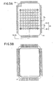
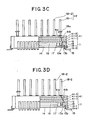
- a package body 11 is made up of a plurality of ceramics layers.
- a chip mounting layer 12 is the uppermost layer in the structure shown in FIGS.3C and 3D.
- the package body 11 also has a wire bonding layer 13, a cap 14, and external connection terminals 15, which are arranged in this order from the chip mounting layer 12. That is, the wire bonding layer 13 is positioned at a level lower than the chip mounting layer 12, and the cap 14 is positioned at a level lower than the wire bonding layer 13.
- the external connection terminals 15 are positioned at a level lower than the cap 14.
- a semiconductor integrated circuit chip 16 (hereafter simply referred to as a chip) such as a silicon chip is fastened to the chip mounting layer 12.
- a chip such as a silicon chip is fastened to the chip mounting layer 12.
- a metallized insulating layer 41 is mounted on a surface of the package body 11 opposite to the cap 14.
- a predetermined number of pin-shaped external connection terminals 18 is mounted by brazing, for example, on the metallized insulating layer 41 so as to elevationally project therefrom.
- the external connection terminals 18 are arranged so as to form a matrix.
- the external connection terminals 18 includes power supply terminals 18-1 and evaluation dedicated terminals 18-2.
- the power supply terminals 18-1 are positioned in the four corners of the matrix arrangement of external connection terminals.
- the metallized insulating layer 41 is made up of three ceramics layers 41-1, 41-2 and 41-3 stacked in this order. Through holes 41a are formed in the layers 41-1, 41-2 and 41-3, and internal connection lines 41b are formed on surfaces thereof.
- the through holes 41a are filled with a conductive material. This conductive material formed in the through holes is served as a part of the internal connection lines 41b. Similarly, through holes and internal connection lines are provided in and on the chip mounting layer 12. Further, through holes 13a filled with a conductive material are formed in the chip mounting layer 12 and the wire bonding layer 13. Internal connection lines 13b are formed on surfaces of the layers 13-1, 13-2 and 13-3.
- the power supply terminals 18-1 are connected to related bonding pads formed on the chip 16 and corresponding power supply lines out of the external connection terminals 15 through the internal connection lines 41b and 13b.
- the evaluation dedicated terminals 18-2 are connected to related bonding pads formed on the chip 16 through the internal connection lines 41b, but are not common to the external connection terminals 15. This means that the evaluation dedicated 18-2 are operationally independent of the external connection terminals 15.
- the external connection terminals 15 are terminals used at the normal operation.
- the external connection terminals 18-2 are terminals used at the time of developing and evaluating integrated circuits formed on the chip 16.
- the evaluation dedicated terminals 18-2 pass signals such as a holt signal, holt acknowledge signal, clock used for single step operation, debug enable signal, program mode select signal, real/write signal used at the time of holt, register rewriting signal used at the time of holt, external access ready signal used at the time of holt, internal/external instruction switching signal, program address input/output signal, and program data input/output signal.
- signals such as a holt signal, holt acknowledge signal, clock used for single step operation, debug enable signal, program mode select signal, real/write signal used at the time of holt, register rewriting signal used at the time of holt, external access ready signal used at the time of holt, internal/external instruction switching signal, program address input/output signal, and program data input/output signal.
- the external connection terminals 18 are arranged in a grid array method so as to form the matrix arrangement. At least, the external connection terminals 18 consists of at least two rows and two columns. For example, the external connection terminals 18 consists of 64 terminals each having a diameter of 0.4 mm, a length of 4.6 mm, and are partitioned in 8 columns each consisting of 8 terminals. A pitch between the neighboring terminals is set equal to 1.778 mm (70 mil), for example. Alternatively, it is possible to arrange the external connection terminals 18 in a desired arrangement.
- the external connection terminals 18 are made of a conductive material such as an alloy of iron and nickel, and an alloy of iron, nickel and cobalt.
- the external connection terminals 18 are mounted on the metallized insulating layer 41 as follows.
- a conductive layer such as a tungsten layer is formed, by screen printing, on the layer 41-3 of the metallized insulating layer 41 made of alumina ceramics.
- the external connection terminals 18 are fastened to the above-mentioned conductive layer by brazing, for example. Thereafter, a nickel plating layer is formed around the surfaces of the external connection terminals 18.
- the power supply terminals 18-1 positioned in the corners of the arrangement are provided with stoppers 18a.
- An index mark 19 indicating the first pin position is formed in one corner of the metallized insulating layer 41.
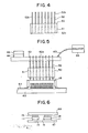
- FIG.5 illustrates an evaluation state where the socket 50 having an insulator plate 51 is attached to the external connection terminals 18. In this evaluation state, a variety of evaluation tests may be done.
- terminals 52 having pin receiving members 52a and projections 52b are fastened to the socket 50.
- the pin receiving members 52 have the same arrangement pattern as the external connection terminals 18.
- Each of the terminals 52 has a stopper 52c.
- the external connection terminals 15 are connected, by soldering, to wiring patterns 61 formed on a surface of a printed circuit board 60.
- the socket 50 is attached to the external connection terminals 18 including the power supply terminals 18-1 and the evaluation dedicated terminals 18-2.
- the terminals 52 are inserted into corresponding pin receiving members 62a formed in an insulator plate 62 of an emulation board.
- Wiring patterns connected to the pin receiving members 62a are formed on a surface of the insulator plate 62.
- a piggy back type socket 64 connected to the wiring patterns.
- a semiconductor device 65 such as a program writer is mounted on the socket 64.
- the wiring patterns are also connected to an emulator or debugger 66 through a coaxial cable 63. In this state, the chip 16 is subjected to a variety of processing for development, evaluation and debug.
- the chip 16 forms a digital signal processor which includes a programmable memory having an address length of 16 bits and an instruction length of a maximum of 30 bits, for example.
- a digital signal processor In order to evaluate such a digital signal processor, it is required to use evaluation dedicated terminals 18-2 amounting to a maximum of 46 bits.
- the evaluation dedicated terminals 18-2 are used for inputting various instructions of a program for use in evaluation supplied from the emulator 66 and outputting addresses being executed thereto.
- the present invention it is possible to provide a number of evaluation dedicated terminals without increasing the package body. Additionally it is easy to visually investigate the contact state. Therefore, the present invention is optimum to semiconductor chips required to use many evaluation dedicated terminals. Further, the present invention contribute to miniaturizing the package accommodating a processor handling a large amount of address and data information.
- the external connection terminals 15 may be used as terminals open to users like the external connection terminals 15.
- FIG.6 Such an alternative is illustrated in FIG.6. Referring to FIG.6, the external connection terminals 15 extending from the packages 11 are mounted on a printed circuit board 67, and the external connection terminals 18 are inserted into corresponding holes formed in a printed circuit board 68 so that the packages 11 are sandwiched between the printed circuit boards 67 and 68.
- the illustrated structure includes a package body 100 and a metallized insulating cap (layer) layer 92.
- the package body 100 is made up of a package mounting layer 90 consisting of three stacked layers 90-1, 90-2 and 90-3, and a wire bonding layer 91 consisting of two stacked layers 91-1 and 91-2.
- Each layer of the package body 100 is formed of ceramics for example.
- a semiconductor integrated circuit chip 93 such as a silicon chip is mounted on the layer 90-3 of the package mounting layer 90.
- Bonding pads formed on the chip 93 are electrically connected, through bonding wire 94, to bonding pads formed on the layer 91-1 of the wire bonding layer 91.
- a plurality of external connection terminals 95 are mounted on the layer 90-1 of the package mounting layer 90 so as to elevationally project therefrom.
- the external connection terminals 95 are connected to related circuits formed on the chip 93 through the bonding wires 94, and internal connection lines 96 formed in the package mounting layer 90.
- the internal connection lines 96 passes through each layer of the package body 100 via through holes formed therein.
- the external connection terminals 95 consist of 64 or more terminals, for example. It is noted that the external connection terminals 95 are inserted into corresponding holes formed in a printed circuit board, and pass various signals used at the time of normal operation.
- Conductive pads 97 are arranged on the layer 91-2 of the bonding wire layer 91, and connected to internal connection lines 98 formed in the wire bonding layer 91.
- the conductive pads 97 are arranged along the four ends of the package body 100, and are partially disposed in a two-column arrangement.
- the metallized insulating cap 92 consists of three stacked layers 92-1, 92-2 and 92-3, each of which is formed of ceramics such as alumina. Through holes 92a and internal connection lines 92b are formed in the metallized insulating cap 92. Conductive pads 99 are formed on the layer 92-1 of the metallized insulating cap 92 so as to have the same arrangement as the conductive pads 97 formed on the layer 91-2 of the wire bonding layer 91. The metallized insulating cap 92 is mounted on the package body 100 in such a way that the conductive pads 99 are laid on the corresponding pads 97.
- a conductive adhesive 101 such as Pb/Sn, Au/Sn and Ag paste is provided around the conductive pads 97 and 99, whereby the metallized insulating cap 92 is fastened to the package body 100.
- External connection terminals 102 including evaluation dedicated terminals 102-2 and power supply terminals 102-1 are provided on the layer 92-3 of the metallized insulating cap 92 so as to elevationally project therefrom.
- the external connection terminals 102 consists of 64 terminals arranged in the form of a matrix. The external connection terminals 102 are electrically connected to related conductive pads 99 through the internal connection lines 92b.
- evaluation dedicated terminals 102-2 out of the external connection terminals 102 are specifically used for the evaluation (debugging), or in other words, are independent of the external connection terminals 95.
- the power supply terminals 102-1 which are arranged in the four corners of the arrangement, are electrically connected to the corresponding power supply terminals among the external connection terminals 95 through internal connection lines 92b and 98 formed in the metallized insulating cap 92 and the package body 100.
- FIG.8A A variation of the metallized insulating cap 92 is illustrated in FIG.8A.
- the variation of the metallization layer 92 has through holes 92c positioned so as to have the same arrangement as the conductive pads 97 of the package body 100 shown in FIG.7B.
- a conductive plating 92d is formed on an inner wall of each of the through holes 92c.
- the conductive plating 92d relating to each of the through holes 92c is connected to the related conductive pad 99.
- the through holes 92c filled with the conductive plating 92d is filled with a conductive material 103. Thereby, it becomes possible to more securely establish the electrical connection between the conductive pads 97 and 99.
- a package 110 has a package body identical to the package body 100 (FIG.7C), and a ceramics lid layer, which is substituted for the metallized insulating cap 92 (FIG.7C), is provided so as to hermetically seal the chip 93.
- a heat sink or fin 111 having a plurality is mounted on the package 110.
- the aforementioned stacked layers may be constructed in a known manufacturing method. For example, through holes and internal connection lines are formed in ceramics sheets before being subjected to sintering (green sheets). Next, the green sheets are stacked and then divided into a plurality of pieces. Then the pieces are sintered.
Landscapes
- Tests Of Electronic Circuits (AREA)
- Testing Of Individual Semiconductor Devices (AREA)
Applications Claiming Priority (4)
| Application Number | Priority Date | Filing Date | Title |
|---|---|---|---|
| JP139424/88 | 1988-06-08 | ||
| JP13942488 | 1988-06-08 | ||
| JP133243/89 | 1989-05-26 | ||
| JP1133243A JPH0284759A (ja) | 1988-06-08 | 1989-05-26 | 半導体装置 |
Publications (2)
| Publication Number | Publication Date |
|---|---|
| EP0346061A2 true EP0346061A2 (de) | 1989-12-13 |
| EP0346061A3 EP0346061A3 (de) | 1991-04-03 |
Family
ID=26467643
Family Applications (1)
| Application Number | Title | Priority Date | Filing Date |
|---|---|---|---|
| EP19890305678 Withdrawn EP0346061A3 (de) | 1988-06-08 | 1989-06-06 | Integrierte Schaltungsanordnung mit einer verbesserten Packungsstruktur |
Country Status (2)
| Country | Link |
|---|---|
| US (1) | US5041899A (de) |
| EP (1) | EP0346061A3 (de) |
Cited By (3)
| Publication number | Priority date | Publication date | Assignee | Title |
|---|---|---|---|---|
| US5041899A (en) * | 1988-06-08 | 1991-08-20 | Fujitsu Limited | Integrated circuit device having an improved package structure |
| WO1991017568A1 (en) * | 1990-04-27 | 1991-11-14 | International Business Machines Corporation | A multi-layer package incorporating a recessed cavity for a semiconductor chip |
| US12170396B2 (en) | 2021-04-19 | 2024-12-17 | Milwaukee Electric Tool Corporation | Systems and methods for tool signal extension |
Families Citing this family (20)
| Publication number | Priority date | Publication date | Assignee | Title |
|---|---|---|---|---|
| KR940006427Y1 (ko) * | 1991-04-12 | 1994-09-24 | 윤광렬 | 독서용 확대경 |
| JPH05102262A (ja) * | 1991-10-03 | 1993-04-23 | Hitachi Ltd | 半導体装置及びそれを実装した実装装置 |
| US5291062A (en) * | 1993-03-01 | 1994-03-01 | Motorola, Inc. | Area array semiconductor device having a lid with functional contacts |
| JP2931741B2 (ja) * | 1993-09-24 | 1999-08-09 | 株式会社東芝 | 半導体装置 |
| US6031723A (en) * | 1994-08-18 | 2000-02-29 | Allen-Bradley Company, Llc | Insulated surface mount circuit board construction |
| US5542175A (en) * | 1994-12-20 | 1996-08-06 | International Business Machines Corporation | Method of laminating and circuitizing substrates having openings therein |
| KR0179834B1 (ko) * | 1995-07-28 | 1999-03-20 | 문정환 | 컬럼형 패키지 |
| US5641944A (en) * | 1995-09-29 | 1997-06-24 | Allen-Bradley Company, Inc. | Power substrate with improved thermal characteristics |
| US5648892A (en) * | 1995-09-29 | 1997-07-15 | Allen-Bradley Company, Inc. | Wireless circuit board system for a motor controller |
| US5670749A (en) * | 1995-09-29 | 1997-09-23 | Allen-Bradley Company, Inc. | Multilayer circuit board having a window exposing an enhanced conductive layer for use as an insulated mounting area |
| US5616888A (en) * | 1995-09-29 | 1997-04-01 | Allen-Bradley Company, Inc. | Rigid-flex circuit board having a window for an insulated mounting area |
| US5949136A (en) * | 1995-10-31 | 1999-09-07 | Hewlett-Packard Company | High performance debug I/O |
| US7321485B2 (en) | 1997-04-08 | 2008-01-22 | X2Y Attenuators, Llc | Arrangement for energy conditioning |
| US7336468B2 (en) | 1997-04-08 | 2008-02-26 | X2Y Attenuators, Llc | Arrangement for energy conditioning |
| US9054094B2 (en) | 1997-04-08 | 2015-06-09 | X2Y Attenuators, Llc | Energy conditioning circuit arrangement for integrated circuit |
| JP2003048066A (ja) * | 2001-08-01 | 2003-02-18 | Sumitomo Electric Ind Ltd | ボールグリッドアレイ素子、及びそれを用いた光通信モジュール |
| JP2008537843A (ja) | 2005-03-01 | 2008-09-25 | エックストゥーワイ アテニュエイターズ,エルエルシー | 内部で重なり合った調整器 |
| JP6233507B2 (ja) * | 2014-05-15 | 2017-11-22 | 富士電機株式会社 | パワー半導体モジュールおよび複合モジュール |
| WO2018212273A1 (ja) * | 2017-05-19 | 2018-11-22 | 株式会社村田製作所 | 積層型電子部品 |
| US10804188B2 (en) * | 2018-09-07 | 2020-10-13 | Intel Corporation | Electronic device including a lateral trace |
Family Cites Families (21)
| Publication number | Priority date | Publication date | Assignee | Title |
|---|---|---|---|---|
| DE2556749A1 (de) * | 1975-12-17 | 1977-06-23 | Bbc Brown Boveri & Cie | Leistungshalbleiterbauelement in scheibenzellenbauweise |
| DE2938567C2 (de) * | 1979-09-24 | 1982-04-29 | Siemens AG, 1000 Berlin und 8000 München | Gehäuse für hochintegrierte Schaltkreise |
| US4338621A (en) * | 1980-02-04 | 1982-07-06 | Burroughs Corporation | Hermetic integrated circuit package for high density high power applications |
| US4387388A (en) * | 1980-07-14 | 1983-06-07 | Ncr Corporation | Package and connector receptacle |
| JPS57201054A (en) * | 1981-06-05 | 1982-12-09 | Nec Corp | Lsi package |
| US4482781A (en) * | 1982-05-17 | 1984-11-13 | National Semiconductor Corporation | Stabilization of semiconductor device package leads |
| JPS58206147A (ja) * | 1982-05-26 | 1983-12-01 | Fujitsu Ltd | 半導体装置モジユ−ル |
| US4608592A (en) * | 1982-07-09 | 1986-08-26 | Nec Corporation | Semiconductor device provided with a package for a semiconductor element having a plurality of electrodes to be applied with substantially same voltage |
| JPS59151443A (ja) * | 1983-02-17 | 1984-08-29 | Fujitsu Ltd | 半導体装置 |
| JPS59181651A (ja) * | 1983-03-31 | 1984-10-16 | Toshiba Corp | 集積回路装置 |
| US4513355A (en) * | 1983-06-15 | 1985-04-23 | Motorola, Inc. | Metallization and bonding means and method for VLSI packages |
| JPS607152A (ja) * | 1983-06-24 | 1985-01-14 | Toshiba Corp | 半導体装置 |
| JPS61177763A (ja) * | 1985-02-04 | 1986-08-09 | Hitachi Ltd | 半導体装置 |
| JPS62136057A (ja) * | 1985-12-09 | 1987-06-19 | Nec Corp | 集積回路パツケ−ジ |
| JPS6362364A (ja) * | 1986-09-03 | 1988-03-18 | Nec Corp | 半導体集積回路パツケ−ジ |
| FR2603739B1 (fr) * | 1986-09-05 | 1988-12-09 | Cimsa Sintra | Boitier de composant electronique muni de broches de connexion comportant un micro-boitier amovible |
| US4839717A (en) * | 1986-12-19 | 1989-06-13 | Fairchild Semiconductor Corporation | Ceramic package for high frequency semiconductor devices |
| US4918513A (en) * | 1987-06-05 | 1990-04-17 | Seiko Epson Corporation | Socket for an integrated circuit chip carrier and method for packaging an integrated circuit chip |
| JPS63305542A (ja) * | 1987-06-06 | 1988-12-13 | Nec Corp | ピングリツドアレイパツケ−ジ |
| JP2755587B2 (ja) * | 1988-02-04 | 1998-05-20 | 株式会社 東芝 | 回路基板 |
| EP0346061A3 (de) * | 1988-06-08 | 1991-04-03 | Fujitsu Limited | Integrierte Schaltungsanordnung mit einer verbesserten Packungsstruktur |
-
1989
- 1989-06-06 EP EP19890305678 patent/EP0346061A3/de not_active Withdrawn
- 1989-06-07 US US07/362,525 patent/US5041899A/en not_active Expired - Fee Related
Cited By (4)
| Publication number | Priority date | Publication date | Assignee | Title |
|---|---|---|---|---|
| US5041899A (en) * | 1988-06-08 | 1991-08-20 | Fujitsu Limited | Integrated circuit device having an improved package structure |
| WO1991017568A1 (en) * | 1990-04-27 | 1991-11-14 | International Business Machines Corporation | A multi-layer package incorporating a recessed cavity for a semiconductor chip |
| US5081563A (en) * | 1990-04-27 | 1992-01-14 | International Business Machines Corporation | Multi-layer package incorporating a recessed cavity for a semiconductor chip |
| US12170396B2 (en) | 2021-04-19 | 2024-12-17 | Milwaukee Electric Tool Corporation | Systems and methods for tool signal extension |
Also Published As
| Publication number | Publication date |
|---|---|
| EP0346061A3 (de) | 1991-04-03 |
| US5041899A (en) | 1991-08-20 |
Similar Documents
| Publication | Publication Date | Title |
|---|---|---|
| US5041899A (en) | Integrated circuit device having an improved package structure | |
| EP0481703B1 (de) | Verbindungssubstrat mit integrierter Schaltung zur programmierbaren Verbindung und Probenuntersuchung | |
| US6144090A (en) | Ball grid array package having electrodes on peripheral side surfaces of a package board | |
| US5780925A (en) | Lead frame package for electronic devices | |
| JP4252491B2 (ja) | 検査機能付きモジュール及びその検査方法。 | |
| US5877548A (en) | Terminal configuration in semiconductor IC device | |
| KR100690922B1 (ko) | 반도체 소자 패키지 | |
| JPH1144732A (ja) | マルチチップモジュール | |
| JP3001481B2 (ja) | 半導体装置およびその製造方法 | |
| KR100435978B1 (ko) | 반도체장치 | |
| JP2005322921A (ja) | バンプテストのためのフリップチップ半導体パッケージ及びその製造方法 | |
| JPH01261849A (ja) | 半導体装置の製造方法 | |
| US4737884A (en) | Semiconductor device module | |
| JPH04196253A (ja) | 半導体装置用パッケージ | |
| JPH0284759A (ja) | 半導体装置 | |
| KR101116325B1 (ko) | 반도체 장치 | |
| EP0849800A1 (de) | Multichip Modul mit unterschiedlich gepackten integrierten Schaltkreisen und Verfahren zu seiner Herstellung | |
| JPS62104149A (ja) | 集積回路チツプ・モジユ−ル | |
| JPS61500879A (ja) | 集積回路メモリ・チップ用フラット・パッケ−ジ | |
| JPH07193164A (ja) | 半導体集積回路装置 | |
| JPS6318688A (ja) | セラミツクパツケ−ジ | |
| JPH08185942A (ja) | 増設用icソケット | |
| US5691243A (en) | Process for manufacturing composite semiconductor device | |
| US7199460B2 (en) | Semiconductor device and method of manufacturing the same | |
| JPS635235Y2 (de) |
Legal Events
| Date | Code | Title | Description |
|---|---|---|---|
| PUAI | Public reference made under article 153(3) epc to a published international application that has entered the european phase |
Free format text: ORIGINAL CODE: 0009012 |
|
| AK | Designated contracting states |
Kind code of ref document: A2 Designated state(s): DE FR GB |
|
| PUAL | Search report despatched |
Free format text: ORIGINAL CODE: 0009013 |
|
| AK | Designated contracting states |
Kind code of ref document: A3 Designated state(s): DE FR GB |
|
| 17P | Request for examination filed |
Effective date: 19910731 |
|
| 17Q | First examination report despatched |
Effective date: 19930325 |
|
| STAA | Information on the status of an ep patent application or granted ep patent |
Free format text: STATUS: THE APPLICATION IS DEEMED TO BE WITHDRAWN |
|
| 18D | Application deemed to be withdrawn |
Effective date: 19931005 |