EP0346102A2 - Festkörperbildaufnahmegerät - Google Patents
Festkörperbildaufnahmegerät Download PDFInfo
- Publication number
- EP0346102A2 EP0346102A2 EP89305757A EP89305757A EP0346102A2 EP 0346102 A2 EP0346102 A2 EP 0346102A2 EP 89305757 A EP89305757 A EP 89305757A EP 89305757 A EP89305757 A EP 89305757A EP 0346102 A2 EP0346102 A2 EP 0346102A2
- Authority
- EP
- European Patent Office
- Prior art keywords
- signal
- signal charges
- light receiving
- solid state
- state image
- Prior art date
- Legal status (The legal status is an assumption and is not a legal conclusion. Google has not performed a legal analysis and makes no representation as to the accuracy of the status listed.)
- Granted
Links
Images







Classifications
-
- H—ELECTRICITY
- H04—ELECTRIC COMMUNICATION TECHNIQUE
- H04N—PICTORIAL COMMUNICATION, e.g. TELEVISION
- H04N25/00—Circuitry of solid-state image sensors [SSIS]; Control thereof
- H04N25/40—Extracting pixel data from image sensors by controlling scanning circuits, e.g. by modifying the number of pixels sampled or to be sampled
- H04N25/46—Extracting pixel data from image sensors by controlling scanning circuits, e.g. by modifying the number of pixels sampled or to be sampled by combining or binning pixels
-
- H—ELECTRICITY
- H04—ELECTRIC COMMUNICATION TECHNIQUE
- H04N—PICTORIAL COMMUNICATION, e.g. TELEVISION
- H04N25/00—Circuitry of solid-state image sensors [SSIS]; Control thereof
- H04N25/70—SSIS architectures; Circuits associated therewith
- H04N25/71—Charge-coupled device [CCD] sensors; Charge-transfer registers specially adapted for CCD sensors
- H04N25/73—Charge-coupled device [CCD] sensors; Charge-transfer registers specially adapted for CCD sensors using interline transfer [IT]
-
- H—ELECTRICITY
- H04—ELECTRIC COMMUNICATION TECHNIQUE
- H04N—PICTORIAL COMMUNICATION, e.g. TELEVISION
- H04N25/00—Circuitry of solid-state image sensors [SSIS]; Control thereof
- H04N25/70—SSIS architectures; Circuits associated therewith
- H04N25/71—Charge-coupled device [CCD] sensors; Charge-transfer registers specially adapted for CCD sensors
- H04N25/745—Circuitry for generating timing or clock signals
Definitions
- the present invention relates to a two-dimensional solid state image sensor, and more particularly to a solid state image sensing device adapted to produce image signals with high resolution and low-level false images using a small number of sampling points within a field.
- the resolution of a solid state image sensor depends generally on the number of pixels integrated in it. For higher resolution it is required that the number of pixels be increased. However, the increase of the pixels in number results in a higher frequency by which pixel signals are read out. This will broaden the signal bandwidth and increase noise. Furthermore, the increase of the pixels in number will decrease the size of each pixel and hence decrease the amount of charge that the pixel can store. The increase in noise and the decrease in maximum amount of stored charge will lower the dynamic range of picture signals.
- a combination of two pixels arranged in the vertical charge transfer direction is changed in even and odd fields and a sum signal of the resultant two pixel signals is output as a video signal, thereby performing interlaced scanning.
- the method aims mainly at reduction of residual images by performing signal storage not at frame intervals but at field intervals. With the method, vertical false signals can be decreased but there is a problem of generation of horizontal false signals as in the prior device.
- a solid state image sensor disclosed in Japanese Patent Early Publication No. 61-133782 can realize a resolution, which is substantially equivalent to that possible with a conventional solid state image sensor having a pixel array of square grid pattern, without increasing the integration of pixels and with lowered pixel-readout frequency. Moreover, the solid state image sensor has a feature that, even if the resolution is increased, the dynamic range can be made great.
- a problem with the device is that the structure is complicated because four signal charge readout gates are required for each pixel and the vertical charge transfer paths have to run in a zigzag.
- a solid state image sensing device in which signals of horizontal pixels are added together and a combination of pixels to be added is changed every field.
- the solid state image sensing device in which a plurality of light receiving elements are arranged in a two-dimensional array and one frame is formed of plural fields, comprises a plurality of signal transfer paths (vertical CCD registers) coupled to the light receiving elements for transferring signal charges sensed by them vertically, a second signal transfer path (horizontal CCD register) for horizontally transferring the signal charges from the first signal transfer paths and an adder section for adding together signal charges from first signal transfer paths adjacent to each other.
- a plurality of signal transfer paths vertical CCD registers
- horizontal CCD register for horizontally transferring the signal charges from the first signal transfer paths
- an adder section for adding together signal charges from first signal transfer paths adjacent to each other.
- the adder section performs the addition of signal charges from the n-th and (n-1)-th ones (n is a positive integer) of the first signal transfer paths and the addition of signal charges from the n-th and (n+1)-th ones in alternate fields.
- signal charges of a plurality of pixels can be added together and the combination of pixels to be added can be changed every field, irrespective of a simple structure in which one signal readout gate is combined with one pixel (a light receiving element and a charge storage section). All the signal charges can be read out within one field. Therefore, sufficiently large signal charge with little noise can be obtained, the dynamic range can be increased and high-quality reproduced images with reduced residual images can be obtained.
- the second signal transfer path can be formed of a horizontal transfer path having stages the number of which is at least half the number of horizontal pixels.
- the frequency for driving horizontal transfer electrodes may be decreased to at least half. This will decrease the signal bandwidth and hence noise.
- the dynamic range can be increased and high-resolution images can be obtained.
- the pixel can have an aperture larger than the pitch of the pixels.
- reproduced images with reduced false signals and improved resolution and sensitivity can be obtained by use of a smaller number of pixels. Since the vertical CCD register can be made more simply than in a prior device, a solid state image sensing device having more pixels can be realized.
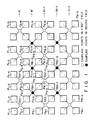
- pixels P1-1, P1-2, ⁇ , P1-N, P2-1, P2-2, ⁇ , P2-N, P3-1, P3-2, ⁇ , P3-N, ⁇ , PM-1, PM-2, ⁇ , PM-N
- o SA1-1, SA1-2, ⁇ , SA2-1,
- SB1-1, SB1-2, ⁇ , SB2-1,...) for a second field.
- Scan lines on a reproduced image are indicated by N, N+1, N+2,... in the first field and by N′, N+1′,... in the second field.
- the pixel sampling points SA2-1, SA2-2 corresponding to the (N+1)-th scan line are likewise respectively detected by adding signal charges from pixels P3-1, P3-2, P4-1 and P4-2 together and by adding signal charges from pixels P3-3, P3-4, P4-3 and P4-4 together. This operation is performed for each of scan lines.
- the pixel sampling points SB1-1, SB1-2 corresponding to the N'th scan line in the second field are respectively detected by adding signal charges from pixels P2-2, P2-3, P3-2 and P3-3 together and by adding signal charges from pixels P2-4, P2-5, P3-4 and P3-5 together. It is to be noted here that, in the first and second fields, the four pixels are added together with one pixel shifted both horizontally and vertically. As a result, the sampling points in the respective fields will be located as indicated by symbols o and ⁇ .
- the number of horizontal transfer electrodes may be half that of prior devices.
- the horizontal transfer frequency may also be halved.
- the horizontal pitch of pixels depends conventionally on the configuration of horizontal transfer electrodes, it does not have to depend on the horizontal transfer electrodes in the present invention. Therefore, the manufacture of the solid state image sensing device becomes easy and a solid state pickup device of a higher resolution becomes feasible.
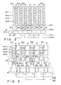
- FIG. 2 is a schematic diagram of a solid state image sensing device according to an embodiment of the present invention
- Fig. 3 illustrates an arrangement of electrodes adapted to add signal charges together.
- the solid state image sensing device comprises pixels (P1-1, P1-2, ⁇ , PM-N) 10, vertical CCD registers (first signal transfer paths) 20 (201-20N), adder electrodes 30, a horizontal CCD register (second signal path) 40, an output amplifier 50 and an output terminal 60.
- Each of vertical CCD registers 20 is a register driven by four-phase clock signals ( ⁇ V1, ⁇ V2, ⁇ V3, ⁇ V4), while horizontal CCD register 40 is driven by two-phase clocks ( ⁇ H2, ⁇ H2).
- adder electrodes 30 use is made of first and second adder electrodes 31 and 32 and partial electrodes of vertical CCD registers 20 (in the present case, electrodes supplied with clocks ⁇ V1, ⁇ V2).
- dotted lines represent signal charge transfer paths.
- Signal charges are read from pixels 10 through field shift gates 21 combined with those transfer electrodes of vertical CCD registers 20 which are supplied with clocks ⁇ V1, ⁇ V3.
- the addition of signals from pixels arranged vertically is performed by timing vertical CCD register 20.
- the addition of pixels arranged horizontally is performed by means of adder electrodes 30.
- adder gate 31 is closed and adder gate 32 is opened.
- signal charge QC1 from register 201 and signal charge QC2 from register 202 are added together at point a as shown.
- adder gate 32 is closed, while adder gate 31 is opened.
- the addition of signal charge QC2 from register 202 and signal charge QC3 from register 203 is performed at point b as shown.
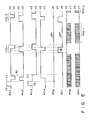
- Fig. 4 is a timing diagram of the operations in the first field
- Fig. 5 is a timing diagram of the operations in the second field
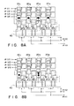
- Figs. 6A and 6B illustrate the addition of vertical pixels
- Figs. 7A, 7B, 8A and 8B illustrate the addition of horizontal pixels.
- V1 to V7 represent predetermined voltages applied to electrodes.
- FS represents a field shift interval during which signal charge is read out of a pixel.
- AD represents an interval during which vertical pixels are added.
- LS1-1, LS1-2, LS2-1 and LS2-2 represent line shift intervals during which signal charges are transferred vertically.
- RO1-1, RO1-2, RO2-1 and RO2-2 represent readout operations of horizontal CCD register 40.
- Fig. 6A illustrates an operating state of the device in the first field in which the timing pulses of Fig. 4 are applied to corresponding electrodes.
- Symbols o represent locations of signal charges.
- Field shift voltage V1 is first applied to ⁇ V1, ⁇ V3 electrodes so that signal charges are read out of two vertical pixels corresponding to those electrodes. The charges from the two vertical pixels are added together during the interval AD. The resultant charges o are transferred up to locations shown in Fig. 7a through the line shift operation.
- adder gate 31 is closed and adder gate 32 is opened with the result that the signal charge transferred through vertical CCD register 201 and the signal charge transferred through vertical CCD register 202 are added together. After signal charges from two horizontal pixels are added together, the resultant charge is transferred to horizontal CCD register 40 and then read out to the outside.
- the timing pulses shown in Fig. 5 are applied to corresponding electrodes and signal charges are represented by ⁇ in Fig. 6B.
- the combination of two pixels to be added is vertically shifted by one pixel from that in the first field.
- adder gate 32 is closed, while adder gate 31 is opened.
- signal charges transferred through vertical CCD registers 202 and 203 are added together. This addition is performed with one pixel shifted horizontally from the first field.
- vertical CCD registers 20 may be made linear and the addition of pixels may be implemented by use of signal transfer paths formed in a simple shape. This will provide a solid state image sensing device with more pixels.
- the number of horizontal transfer stages may be halved for the same resolution.
- the horizontal transfer frequency may also be halved.
- the signal bandwidth can be lowered and noise is reduced correspondingly, resulting in great dynamic range. Further strictlymore, there is an advantage that high-quality pictures which are reduced in residual images can be obtained because all the pixels store signal charges and they are read out every field.
- Fig. 9 illustrates the main part of the embodiment.
- Fig. 10 is a timing diagram of transfer pulses ⁇ H1 and ⁇ H2 applied to transfer electrodes of horizontal CCD register 40.
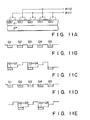
- Figs. 11A to 11E illustrate the transfer of charge through the horizontal CCD register. This embodiment is arranged such that signal charge is transferred from vertical CCD registers 20 to the transfer electrodes of horizontal CCD register 40 which are supplied with pulses ⁇ H1 and ⁇ H2. That area in the register which is indicated in dotted lines represents a signal transfer path.
- ⁇ V1, ⁇ V2, ⁇ V3 and ⁇ V4 represent pulses applied to the transfer electrodes of vertical CCD register 20, while ⁇ H1, ⁇ H2 pulses are applied to the transfer electrodes of horizontal CCD register 40.
- Q1 to Q5 represent signal charges transferred from vertical CCD registers 20, each of them resulting from the addition of signal charges from two vertical pixels.
- Pixels Q1 to Q5 transferred from vertical CCD registers 201 to 205 to horizontal CCD register 40 are added during a horizontal blanking interval as shown in the timing diagram of Fig. 10.
- signal charges of vertical pixels are transferred horizontally and independently.
- ⁇ H1 and ⁇ H2 are both at H level, and the state of charge in register 40 is illustrated in Fig. 11B.
- ⁇ H2 goes to L level, while ⁇ H1 remains at H level.
- two signal charges are added together as Q1+Q2, Q3+Q4,... as shown in Fig. 11C.
- pulses ⁇ H1 and ⁇ H2 first go to H level as is the case with the first field with the result that signal charges from vertical CCD registers 20 are transferred horizontally.
- the state of signal charges at this point is the same as that of Fig. 11B as shown in Fig. 11D.
- Pulse ⁇ H2 goes to L level, while pulse ⁇ H2 remains at H level as opposed to the first field.
- two signal charges are added as Q2+Q3, Q4+Q5,... as shown in Fig. 11E with one pixel shifted horizontally from the case of the first field.
- pixels each resulting from addition of two vertical pixels are added horizontally in units of two pixels. That is, pixels of a two-by-two array are added together to form one pixel with the result that the sampling points described in connection with Fig. 1 are obtained.
- the present embodiment therefore, there is no need for the particular provision of the adder electrodes adapted to add signal charges horizontally, thus simplifying the construction of the device. It goes without saying that the present embodiment can achieve the same advantages as the previous embodiment.
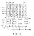
- charge storage sections 70 adapted to store signal charges using interline transfer structure CCDs are formed in the optically sensitive imaging area and a frame inter-line transfer type CCD with a horizontal CCD register has the device structure according to present invention.
- the structure is characterized in that adder electrodes 30 are provided between vertical CCD registers 20 and charge storage sections 70. Owing to this structure the number of transfer stages in charge storage section 70 and horizontal CCD register 40 can be halved.
- the addition of signal charges is performed in the same manner as the embodiment of Fig. 2.
- the present invention need not be limited to the above embodiments.
- the combination of pixels to be added is not limited to that described in connection with Fig. 1.
- Fig. 1 there is illustrated an example in which two first and second fields form one frame of picture
- the present invention may be applied to a case where four first, second, third and fourth fields form one frame as shown in Figs. 13 and 14. If one frame is formed of four fields, the moire will be decreased further and the number of effective sampling points will increase. This will offer a further improvement in resolution.
- arrows indicate combinations of pixels to be added.
- Symbol o represents sampling points in the first field, ⁇ sampling points in the second field, ⁇ sampling points in the third field and ⁇ sampling points in the fourth field. Such sampling points can be obtained in the same manner as that described in connection with Figs. 2 to 12.
- the present invention may also be applied to a frame-storage charge transfer CCD, an MOS solid state image sensing device, a line address solid state image sensing device or the like.
- a frame-storage charge transfer CCD an MOS solid state image sensing device
- a line address solid state image sensing device or the like.
- the present invention it is necessary only that signal charges be read out of all the pixels within one field.
- the MOS solid state image sensing device the first and second signal paths are used as signal lines and MOS gates are placed between the signal lines and light-receiving elements. By controlling the timing of on and off of the MOS gates, it is possible to perform the same add process as in the above embodiments.
- the present invention may also be applied to a solid state image sensing device of a two-layer structure using a photoelectric conversion film made of, for example, amorphous silicon as the light receiving surface.
- a photoelectric conversion film made of, for example, amorphous silicon
- the aperture of the device itself can be made large.
- the moire will be decreased further and the sensitivity will be improved, resulting in a significant improvement in picture quality.
- the present invention may be modified in various ways without departing from the scope of the invention.
- the adder electrodes are arranged between the first signal paths and the second signal path, the addition of signal charges of horizontal pixels can be made and the combination of the pixels to be added can be changed every field, irrespective of a simple construction in which one signal readout gate is used with one pixel. Therefore, the reduction in dynamic range with an increase in the number of pixels and the generation of false signals which produce the moire can be prevented without giving rise to complication in device structure. It thus becomes possible to realize a solid state image sensing device of high resolution and simple construction.
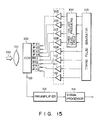
- Fig. 15 shows a schematic arrangement of a pickup device using the solid state imaging device of Fig. 2 and operating in the manner illustrated in Figs. 4 to 8B.
- An input optical image 100 is imaged onto a solid state image sensing device 102 by an objective lens 101.
- To solid state image sensing device 102 are applied clock pulses ⁇ V1, ⁇ V2, ⁇ V3, ⁇ V4, BG1, BG2, ⁇ H1 and ⁇ H2 which are shown in Figs. 4 and 5.
- These clock pulses are output from drivers 105 to 112 of a clock driver circuit.
- Clock drivers 105 to 108 are output from a three-valued level producing circuit 104, which is responsive to timing pulses output from a timing pulse generating circuit 103 to produce three-valued pulses necessary for driving the vertical CCD registers in solid state image sensing device 102.
- the three-valued pulses may readily be formed by using an analog multiplexer.
- Clock drivers 109 to 112 are responsive to timing pulses from timing pulse generating circuit 103 to apply pulses BG2, BG2, ⁇ H1 and ⁇ H2.
- Output terminal OS of solid state image sensing device 102 is connected to an input terminal of a preamplifier 113,and an image signal output from the solid state image sensing device is amplified by preamplifier 113 and then applied to a signal processor 114.
- Signal processor 114 performs impedance conversion, gamma correction, white clipping, etc. on the image signal to provide a TV signal.
- Fig. 16 shows a schematic arrangement of a pickup device using the solid state imaging device of Fig. 9 and operating in the manner illustrated in Fig. 10 and Figs. 11A to 11E.
- An input optical image 200 is imaged onto a solid state image sensing device 202 by an objective lens 201.
- To solid state image sensing device 202 are applied clock pulses ⁇ H1 and ⁇ H2 shown in Fig. 10 and vertical CCD register driving pulses ⁇ V1, ⁇ V2, ⁇ V3 and ⁇ V4 which are shown in Figs. 4 and 5. These clock pulses are output from drivers 205 to 210 of a clock driver circuit.
- Clock drivers 205 to 208 are supplied with three-valued pulses from three-valued level pulse producing circuit 204. The three-valued pulses are produced from timing pulses output from a timing pulse generating circuit 203 and used for driving the vertical CCD registers in solid state image sensing device 102.
- Fig. 16 eliminates the need for clock pulses BG1 and BG2 in the arrangement of Fig. 15 and thus becomes more simple in construction.
- Output terminal OS of solid state image sensing device 202 is connected to an input terminal of a preamplifier 211, and an image signal output from the solid state image sensing device is amplified by preamplifier 211 and then applied to a signal processor 212.
- Signal processor 212 performs impedance conversion, gamma correction, white clipping, etc. on the image signal to provide a TV signal.
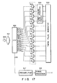
- Fig. 17 illustrates a circuit arrangement of a pickup device equipped with a solid state image sensing device using the frame interline charge transfer CCD shown in Fig. 12.
- clock pulses ⁇ V1, ⁇ V2, ⁇ V3, ⁇ V4, BG1, BG2, ⁇ S1, ⁇ S2, ⁇ S3, ⁇ S4, ⁇ H1, ⁇ H2, are applied from clock drivers 305 to 316 to solid state image sensing device 302.
- Three-valued level producing circuit 304 forms three-valued pulses necessary for driving the vertical CCD registers in solid state image sensing device 302.
- Timing signal generating circuit 303 produces required timing pulses.
- An image signal output from solid state image sensing device 302 is amplified by preamplifier 317 and then applied to signal processor 318.
- Signal processor 318 performs processes such as impedance conversion, gamma correction and white clipping on the image signal to provide a TV signal.
Landscapes
- Engineering & Computer Science (AREA)
- Multimedia (AREA)
- Signal Processing (AREA)
- Transforming Light Signals Into Electric Signals (AREA)
- Solid State Image Pick-Up Elements (AREA)
Applications Claiming Priority (2)
| Application Number | Priority Date | Filing Date | Title |
|---|---|---|---|
| JP63139519A JP2735223B2 (ja) | 1988-06-08 | 1988-06-08 | 固体撮像装置 |
| JP139519/88 | 1988-06-08 |
Publications (3)
| Publication Number | Publication Date |
|---|---|
| EP0346102A2 true EP0346102A2 (de) | 1989-12-13 |
| EP0346102A3 EP0346102A3 (de) | 1992-04-29 |
| EP0346102B1 EP0346102B1 (de) | 1995-08-23 |
Family
ID=15247182
Family Applications (1)
| Application Number | Title | Priority Date | Filing Date |
|---|---|---|---|
| EP89305757A Expired - Lifetime EP0346102B1 (de) | 1988-06-08 | 1989-06-07 | Festkörperbildaufnahmegerät |
Country Status (4)
| Country | Link |
|---|---|
| US (1) | US4996600A (de) |
| EP (1) | EP0346102B1 (de) |
| JP (1) | JP2735223B2 (de) |
| DE (1) | DE68923909T2 (de) |
Cited By (8)
| Publication number | Priority date | Publication date | Assignee | Title |
|---|---|---|---|---|
| EP0498662A3 (en) * | 1991-02-08 | 1992-09-23 | Sharp Kabushiki Kaisha | A method of reading out signals for a solid-state imaging device |
| EP0509661A3 (en) * | 1991-03-29 | 1993-01-13 | Sharp Kabushiki Kaisha | Method of driving interline transfer type ccd imager |
| EP0553869A3 (de) * | 1992-01-31 | 1994-02-16 | Toshiba Kk | |
| EP0896468A3 (de) * | 1997-08-07 | 2000-05-17 | Nec Corporation | Festkörperbildaufnahmevorrichtung und Ansteuermethode dafür |
| EP1176808A2 (de) | 2000-07-27 | 2002-01-30 | Canon Kabushiki Kaisha | Bildaufnahmevorrichtung |
| DE19642427C2 (de) * | 1995-10-17 | 2002-11-07 | Protek Japan Corp | Bilderzeugungsschaltkreis |
| EP1091411A3 (de) * | 1999-10-07 | 2004-01-28 | Fuji Photo Film Co., Ltd. | Festkörperbildaufnahmevorrichtung |
| EP1416424A3 (de) * | 2002-10-30 | 2007-01-10 | Microsoft Corporation | Fotosensorarray mit Pixel-Ebene Signalvergleich |
Families Citing this family (29)
| Publication number | Priority date | Publication date | Assignee | Title |
|---|---|---|---|---|
| US5262871A (en) * | 1989-11-13 | 1993-11-16 | Rutgers, The State University | Multiple resolution image sensor |
| JP2662455B2 (ja) * | 1990-09-13 | 1997-10-15 | シャープ株式会社 | 固体撮像装置 |
| JPH0514816A (ja) * | 1991-06-28 | 1993-01-22 | Sharp Corp | 固体撮像装置およびその駆動方法 |
| US5539536A (en) * | 1992-03-19 | 1996-07-23 | Sony Corporation | Linear imaging sensor having improved charged transfer circuitry |
| US5264939A (en) * | 1992-05-29 | 1993-11-23 | Eastman Kodak Company | Apparatus and method for generating an interlaced viewing signal from the output signal of a non-interlaced camera system |
| US5395374A (en) * | 1993-09-02 | 1995-03-07 | Danek Medical, Inc. | Orthopedic cabling method and apparatus |
| JP3242515B2 (ja) * | 1993-12-24 | 2001-12-25 | キヤノン株式会社 | 撮像装置 |
| US5625414A (en) * | 1995-01-30 | 1997-04-29 | Eastman Kodak Company | Imaging device using asymmetrical timing for pixel summing |
| US5874993A (en) * | 1995-04-21 | 1999-02-23 | Eastman Kodak Company | Solid state image sensor with selectable resolution |
| JPH11234569A (ja) * | 1998-02-13 | 1999-08-27 | Sony Corp | 固体撮像装置の駆動方法及び固体撮像素子、並びにカメラ |
| JP3819631B2 (ja) * | 1999-03-18 | 2006-09-13 | 三洋電機株式会社 | 固体撮像装置 |
| US7106374B1 (en) | 1999-04-05 | 2006-09-12 | Amherst Systems, Inc. | Dynamically reconfigurable vision system |
| US6693670B1 (en) * | 1999-07-29 | 2004-02-17 | Vision - Sciences, Inc. | Multi-photodetector unit cell |
| US7084905B1 (en) * | 2000-02-23 | 2006-08-01 | The Trustees Of Columbia University In The City Of New York | Method and apparatus for obtaining high dynamic range images |
| EP1303978A4 (de) * | 2000-07-05 | 2006-08-09 | Vision Sciences Inc | Verfahren zur komprimierung des dynamikbereiches |
| WO2002043366A2 (en) * | 2000-11-27 | 2002-05-30 | Vision Sciences Inc. | Programmable resolution cmos image sensor |
| US7432971B2 (en) * | 2002-06-21 | 2008-10-07 | Shimadzu Corporation | In-situ storage image sensor and in-situ storage image pickup apparatus |
| JP3848650B2 (ja) | 2002-11-12 | 2006-11-22 | 松下電器産業株式会社 | 固体撮像素子およびこれを備えたカメラ |
| JP4551085B2 (ja) * | 2003-12-01 | 2010-09-22 | パナソニック株式会社 | 固体撮像装置、撮像装置 |
| JP4306603B2 (ja) * | 2004-12-20 | 2009-08-05 | ソニー株式会社 | 固体撮像装置および固体撮像装置の駆動方法 |
| JP4678583B2 (ja) * | 2005-03-25 | 2011-04-27 | 日本ビクター株式会社 | 固体撮像装置 |
| JP4457961B2 (ja) * | 2005-04-28 | 2010-04-28 | ソニー株式会社 | 固体撮像素子 |
| AU2008211541B2 (en) | 2007-01-29 | 2012-03-08 | Powermat Technologies Ltd. | Pinless power coupling |
| JP2008244738A (ja) * | 2007-03-27 | 2008-10-09 | Fujifilm Corp | 撮像装置および撮像素子の駆動制御方法 |
| JP2009070902A (ja) * | 2007-09-11 | 2009-04-02 | Fujifilm Corp | 撮像素子及び撮像装置 |
| JP4869302B2 (ja) * | 2008-08-22 | 2012-02-08 | 株式会社東芝 | 画像処理装置及び画像処理方法 |
| US7948534B2 (en) * | 2008-10-22 | 2011-05-24 | Eastman Kodak Company | Charge-coupled device image sensor with vertical binning of same-color pixels |
| JP2011109219A (ja) * | 2009-11-13 | 2011-06-02 | Mitsubishi Electric Corp | 画像信号処理装置及び方法 |
| WO2013051190A1 (ja) * | 2011-10-07 | 2013-04-11 | シャープ株式会社 | 固体撮像装置および電子情報機器 |
Family Cites Families (8)
| Publication number | Priority date | Publication date | Assignee | Title |
|---|---|---|---|---|
| US3932775A (en) * | 1974-07-25 | 1976-01-13 | Rca Corporation | Interlaced readout of charge stored in a charge coupled image sensing array |
| JPS593066B2 (ja) * | 1975-09-18 | 1984-01-21 | ソニー株式会社 | コタイサツゾウタイ |
| DE3220667A1 (de) * | 1982-06-02 | 1983-12-08 | Canon K.K., Tokyo | Festkoerper-bildaufnahmeelement |
| JPS61179679A (ja) * | 1985-02-05 | 1986-08-12 | Fuji Photo Film Co Ltd | 電荷転送型固体撮像装置 |
| JPS62159579A (ja) * | 1986-01-07 | 1987-07-15 | Hitachi Ltd | 固体撮像装置 |
| JPH0644823B2 (ja) * | 1986-08-22 | 1994-06-08 | 日本ビクター株式会社 | 固体撮像装置 |
| EP0286122A3 (de) * | 1987-04-10 | 1990-04-25 | Kabushiki Kaisha Toshiba | Festkörper-Bildaufnahmevorrichtung mit hoher Geschwindigkeitsverblendungsfunktion |
| US4897728A (en) * | 1987-10-09 | 1990-01-30 | Kabushiki Kaisha Toshiba | Charge transfer device for solid state image pickup apparatus and method of driving the same |
-
1988
- 1988-06-08 JP JP63139519A patent/JP2735223B2/ja not_active Expired - Lifetime
-
1989
- 1989-06-07 DE DE68923909T patent/DE68923909T2/de not_active Expired - Lifetime
- 1989-06-07 EP EP89305757A patent/EP0346102B1/de not_active Expired - Lifetime
- 1989-06-08 US US07/363,085 patent/US4996600A/en not_active Expired - Lifetime
Cited By (16)
| Publication number | Priority date | Publication date | Assignee | Title |
|---|---|---|---|---|
| EP0498662A3 (en) * | 1991-02-08 | 1992-09-23 | Sharp Kabushiki Kaisha | A method of reading out signals for a solid-state imaging device |
| EP0509661A3 (en) * | 1991-03-29 | 1993-01-13 | Sharp Kabushiki Kaisha | Method of driving interline transfer type ccd imager |
| EP0553869A3 (de) * | 1992-01-31 | 1994-02-16 | Toshiba Kk | |
| US5459509A (en) * | 1992-01-31 | 1995-10-17 | Kabushiki Kaisha Toshiba | Method for transferring charge, charge transfer device and solid state image sensing device using the same |
| DE19642427C2 (de) * | 1995-10-17 | 2002-11-07 | Protek Japan Corp | Bilderzeugungsschaltkreis |
| EP0896468A3 (de) * | 1997-08-07 | 2000-05-17 | Nec Corporation | Festkörperbildaufnahmevorrichtung und Ansteuermethode dafür |
| US6185270B1 (en) | 1997-08-07 | 2001-02-06 | Nec Corporation | Solid state imaging device and method for driving the same |
| EP1091411A3 (de) * | 1999-10-07 | 2004-01-28 | Fuji Photo Film Co., Ltd. | Festkörperbildaufnahmevorrichtung |
| EP1176808A3 (de) * | 2000-07-27 | 2003-01-02 | Canon Kabushiki Kaisha | Bildaufnahmevorrichtung |
| EP1176808A2 (de) | 2000-07-27 | 2002-01-30 | Canon Kabushiki Kaisha | Bildaufnahmevorrichtung |
| US7071980B2 (en) | 2000-07-27 | 2006-07-04 | Canon Kabushiki Kaisha | Image sensing apparatus |
| US7630010B2 (en) | 2000-07-27 | 2009-12-08 | Canon Kabushiki Kaisha | Image sensing apparatus having an adding circuit to provide a one-pixel signal from a plurality of photoelectric conversion sections |
| US7639295B2 (en) | 2000-07-27 | 2009-12-29 | Canon Kabushiki Kaisha | Image sensing apparatus |
| US7920195B2 (en) | 2000-07-27 | 2011-04-05 | Canon Kabushiki Kaisha | Image sensing apparatus having an effective pixel area |
| US8531568B2 (en) | 2000-07-27 | 2013-09-10 | Canon Kabushiki Kaisha | Image sensing apparatus with shielding for unit blocks of a common processing circuit of plural pixels |
| EP1416424A3 (de) * | 2002-10-30 | 2007-01-10 | Microsoft Corporation | Fotosensorarray mit Pixel-Ebene Signalvergleich |
Also Published As
| Publication number | Publication date |
|---|---|
| EP0346102B1 (de) | 1995-08-23 |
| DE68923909T2 (de) | 1996-01-11 |
| JP2735223B2 (ja) | 1998-04-02 |
| EP0346102A3 (de) | 1992-04-29 |
| DE68923909D1 (de) | 1995-09-28 |
| JPH01309579A (ja) | 1989-12-13 |
| US4996600A (en) | 1991-02-26 |
Similar Documents
| Publication | Publication Date | Title |
|---|---|---|
| US4996600A (en) | Two dimensional solid state image sensing device | |
| JP3511772B2 (ja) | 固体撮像素子、固体撮像素子の駆動方法、カメラ装置及びカメラシステム | |
| CN100387050C (zh) | 固态成像装置、用于固态成像装置的方法、成像方法和成像器 | |
| EP0498662B1 (de) | Ein Verfahren zum Auslesen von Signalen aus einer Festkörper-Bildaufnahmevorrichtung | |
| US7701498B2 (en) | Solid-state image pickup device, drive method therefor and camera | |
| JP4078741B2 (ja) | 固体撮像装置およびその駆動方法並びにカメラシステム | |
| JP3102557B2 (ja) | 固体撮像素子およびその駆動方法 | |
| JP3459738B2 (ja) | 撮像装置 | |
| JP2009521842A (ja) | 静止画またはビデオ撮影用画像センサ | |
| JPH11146408A (ja) | 固体撮像装置及びその電荷読み出し方法 | |
| JP2856854B2 (ja) | 固体撮像装置 | |
| US7697048B2 (en) | Solid state imaging apparatus and driving method of the solid state imaging apparatus using four pixel addition | |
| JPH09233394A (ja) | 撮像装置 | |
| US20070085924A1 (en) | Control circuit for reading out signal charges from main and subsidiary pixels of a solid-state image sensor separately from each other in interlace scanning | |
| JPH0514816A (ja) | 固体撮像装置およびその駆動方法 | |
| JP2799003B2 (ja) | 固体撮像素子の駆動方式 | |
| JPH09298755A (ja) | 固体撮像素子 | |
| JPH0595515A (ja) | 固体撮像装置 | |
| JP3500729B2 (ja) | 固体撮像装置 | |
| JPH10200819A (ja) | 固体撮像装置およびその駆動方法並びにカメラ | |
| JPH0332176A (ja) | 固体撮像素子とその駆動方法 | |
| JP2753895B2 (ja) | 固体撮像装置 | |
| JP2595916B2 (ja) | 固体撮像素子及びその駆動方法 | |
| JP2666398B2 (ja) | 固体撮像素子及びその駆動方法 | |
| JPS5834996B2 (ja) | カラ−コタイサツゾウソウチ |
Legal Events
| Date | Code | Title | Description |
|---|---|---|---|
| PUAI | Public reference made under article 153(3) epc to a published international application that has entered the european phase |
Free format text: ORIGINAL CODE: 0009012 |
|
| 17P | Request for examination filed |
Effective date: 19890623 |
|
| AK | Designated contracting states |
Kind code of ref document: A2 Designated state(s): DE FR GB |
|
| PUAL | Search report despatched |
Free format text: ORIGINAL CODE: 0009013 |
|
| AK | Designated contracting states |
Kind code of ref document: A3 Designated state(s): DE FR GB |
|
| 17Q | First examination report despatched |
Effective date: 19940302 |
|
| GRAA | (expected) grant |
Free format text: ORIGINAL CODE: 0009210 |
|
| AK | Designated contracting states |
Kind code of ref document: B1 Designated state(s): DE FR GB |
|
| REF | Corresponds to: |
Ref document number: 68923909 Country of ref document: DE Date of ref document: 19950928 |
|
| ET | Fr: translation filed | ||
| PLBE | No opposition filed within time limit |
Free format text: ORIGINAL CODE: 0009261 |
|
| STAA | Information on the status of an ep patent application or granted ep patent |
Free format text: STATUS: NO OPPOSITION FILED WITHIN TIME LIMIT |
|
| 26N | No opposition filed | ||
| REG | Reference to a national code |
Ref country code: GB Ref legal event code: IF02 |
|
| PGFP | Annual fee paid to national office [announced via postgrant information from national office to epo] |
Ref country code: DE Payment date: 20080828 Year of fee payment: 20 |
|
| PGFP | Annual fee paid to national office [announced via postgrant information from national office to epo] |
Ref country code: FR Payment date: 20080507 Year of fee payment: 20 |
|
| PGFP | Annual fee paid to national office [announced via postgrant information from national office to epo] |
Ref country code: GB Payment date: 20080611 Year of fee payment: 20 |
|
| REG | Reference to a national code |
Ref country code: GB Ref legal event code: PE20 Expiry date: 20090606 |
|
| PG25 | Lapsed in a contracting state [announced via postgrant information from national office to epo] |
Ref country code: GB Free format text: LAPSE BECAUSE OF EXPIRATION OF PROTECTION Effective date: 20090606 |