EP0348539A1 - Réseau logique programmable CMOS - Google Patents
Réseau logique programmable CMOS Download PDFInfo
- Publication number
- EP0348539A1 EP0348539A1 EP88110267A EP88110267A EP0348539A1 EP 0348539 A1 EP0348539 A1 EP 0348539A1 EP 88110267 A EP88110267 A EP 88110267A EP 88110267 A EP88110267 A EP 88110267A EP 0348539 A1 EP0348539 A1 EP 0348539A1
- Authority
- EP
- European Patent Office
- Prior art keywords
- line
- row
- area
- dummy
- column
- Prior art date
- Legal status (The legal status is an assumption and is not a legal conclusion. Google has not performed a legal analysis and makes no representation as to the accuracy of the status listed.)
- Withdrawn
Links
- 239000003990 capacitor Substances 0.000 claims abstract description 9
- 239000000758 substrate Substances 0.000 claims description 4
- 230000000295 complement effect Effects 0.000 claims description 3
- 230000005669 field effect Effects 0.000 claims description 3
- 229920000747 poly(lactic acid) Polymers 0.000 description 7
- 238000010586 diagram Methods 0.000 description 4
- 230000005540 biological transmission Effects 0.000 description 2
- 238000011156 evaluation Methods 0.000 description 2
- 238000004519 manufacturing process Methods 0.000 description 2
- XAGFODPZIPBFFR-UHFFFAOYSA-N aluminium Chemical compound [Al] XAGFODPZIPBFFR-UHFFFAOYSA-N 0.000 description 1
- 229910052782 aluminium Inorganic materials 0.000 description 1
- 230000001419 dependent effect Effects 0.000 description 1
- 230000007257 malfunction Effects 0.000 description 1
- 229910021420 polycrystalline silicon Inorganic materials 0.000 description 1
Images
Classifications
-
- H—ELECTRICITY
- H03—ELECTRONIC CIRCUITRY
- H03K—PULSE TECHNIQUE
- H03K5/00—Manipulating of pulses not covered by one of the other main groups of this subclass
- H03K5/13—Arrangements having a single output and transforming input signals into pulses delivered at desired time intervals
- H03K5/14—Arrangements having a single output and transforming input signals into pulses delivered at desired time intervals by the use of delay lines
-
- G—PHYSICS
- G11—INFORMATION STORAGE
- G11C—STATIC STORES
- G11C7/00—Arrangements for writing information into, or reading information out from, a digital store
- G11C7/22—Read-write [R-W] timing or clocking circuits; Read-write [R-W] control signal generators or management
-
- H—ELECTRICITY
- H03—ELECTRONIC CIRCUITRY
- H03K—PULSE TECHNIQUE
- H03K19/00—Logic circuits, i.e. having at least two inputs acting on one output; Inverting circuits
- H03K19/02—Logic circuits, i.e. having at least two inputs acting on one output; Inverting circuits using specified components
- H03K19/173—Logic circuits, i.e. having at least two inputs acting on one output; Inverting circuits using specified components using elementary logic circuits as components
- H03K19/177—Logic circuits, i.e. having at least two inputs acting on one output; Inverting circuits using specified components using elementary logic circuits as components arranged in matrix form
- H03K19/17704—Logic circuits, i.e. having at least two inputs acting on one output; Inverting circuits using specified components using elementary logic circuits as components arranged in matrix form the logic functions being realised by the interconnection of rows and columns
- H03K19/17708—Logic circuits, i.e. having at least two inputs acting on one output; Inverting circuits using specified components using elementary logic circuits as components arranged in matrix form the logic functions being realised by the interconnection of rows and columns using an AND matrix followed by an OR matrix, i.e. programmable logic arrays
- H03K19/17716—Logic circuits, i.e. having at least two inputs acting on one output; Inverting circuits using specified components using elementary logic circuits as components arranged in matrix form the logic functions being realised by the interconnection of rows and columns using an AND matrix followed by an OR matrix, i.e. programmable logic arrays with synchronous operation, i.e. using clock signals, e.g. of I/O or coupling register
- H03K19/1772—Logic circuits, i.e. having at least two inputs acting on one output; Inverting circuits using specified components using elementary logic circuits as components arranged in matrix form the logic functions being realised by the interconnection of rows and columns using an AND matrix followed by an OR matrix, i.e. programmable logic arrays with synchronous operation, i.e. using clock signals, e.g. of I/O or coupling register with synchronous operation of at least one of the logical matrixes
Definitions
- the invention relates to the improvement of non-overlapping two-phase clocked, technically complementary insulating layer field-effect transistors, programmable Lokig fields, i.e. abbreviated CMOS-PLAs, as described in the book by N.H.E. Weste et al "Principles of CMOS-VLSI Design", Reading, Massachusetts, 1985, pages 368-373, in particular chapter 8.7.4 (pages 372/373).
- CMOS-PLAs programmable Lokig fields
- CMOS-PLAs have an AND area, an OR area and an AND / OR area connecting these two to each other, their respective transistors in m rows and n columns of the AND area and in p columns of the OR area between each a first and a second row line or between a first and a second column line.
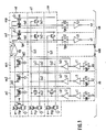
- the internal clocking serves a dummy line in the AND and AND / OR area, which also has two line lines, and a Schmitt trigger, the input of which is connected to the first line line of the dummy line.
- a precharge P transistor and an Evaluate N transistor are provided, the gates of which in the rows and in the dummy row are inverted by the first two-phase transistor. Clock or in the columns are driven by the output signal of the Schmitt trigger.
- the respective controlled current path of the precharge P transistors between an operating voltage and the first row or column line and that of the Evaluate N transistor between the circuit zero and the second row or column line.
- two N-transistors are provided in the dummy row in the AND area, the controlled current paths of which lie between the first and the second row line and of which the gate of the one with the first column line and the gate of the other with the second column line connected is.
- CMOS-PLA complementary metal-oxide-semiconductor
- one of the phases of the non-overlapping two-phase clock is used to store the input signals in the AND region, while an internal clock signal by means of the dummy line and the one mentioned is used for clocking the OR region Schmitt triggers is generated.
- This must have a greater delay than the evaluation time in each line of the AND and OR areas. This is determined by the respective load capacitance and the area of the row and column transistors.
- the load capacitance essentially consists of the capacitance of the source or drain zones of these transistors.
- the number of line transistors is greatest when there is a line transistor between each input of the CMOS-PLA, ie either the non-inverted or inverted input signal, and the corresponding minterm.
- the greatest evaluation time arises if, in such a term, only one line transistor has to reload the line capacitance due to the input signals.
- the dummy line and the Schmitt trigger are provided in the CMOS-PLA described above. Due to the transistors in the dummy line, the load capacity of this line is twice as large as that of the worst case explained within the AND range.
- CMOS PLAs manufactured as integrated circuits manufacturing process-dependent fluctuations in the delay.
- the invention now seeks to remedy this, the task of which is to modify and improve the above-described CMOS PLA in such a way that the production-related delay fluctuations are substantially reduced.
- the Schmitt trigger is also to be replaced by a subcircuit having fewer transistors.
- the columns us1, us2, usn are shown in the drawings from the n columns of the AND region, while the columns os1, osp are shown from the p columns of the OR region.
- the lines z1, zm and additionally the dummy line zd can be seen in FIG. 1.
- the AND / OR area uob lies between the AND area ub and the OR area ob.
- Each row has the two row lines lz1, lz2, the latter only being present in the AND area, but the former leading into the OR area, usually with two inverters connected in series in terms of signal flow in the AND / OR area, via which the signal of the row line lz1 is carried to refresh the level.
- the columns also each have the two column lines ls1, ls2.
- Those of the AND area carry the non-inverted and the inverted input signal, which leads from the respective input e1, e2, en via the respective input transmission gate tge, which is controlled by the first clock signal f1, and via the two inverters i1, i2 is.
- the first column line ls1 lies at the output of the inverter i1 and the second column line ls2 lies at that of the second inverter i2.
- the first column line ls1 lies via the output transmission gate tga, which is controlled by the second clock signal f2, and the third inverter i3 at the respective output a1, ap.
- the dummy line zd also has the in the AND area two row lines ld1, ld2, of which the first row line ld1 is connected to one input of the NOR gate ng, while the other input of which is connected to the reset line lr.
- the pre-charge P transistor tpz, tps is provided, the controlled current path of which connects the respective first row line lz1, ld1 and the respective column line ls1 to the operating voltage source u. Furthermore, in each row, the dummy row and each column of the OR area, there is provided whether the evaluate-N transistor tez, tes, whose controlled current path connects the respective second row or column line lz2, ld2, ls2 to the circuit zero. In each line and in the dummy line, the gates of the two transistors tpz, tez are connected to one another and driven by the inverted first clock signal f1q. In each column of the OR area ob, the gates of the two transistors tps, tes are also connected to one another, but are driven by the output of the OR gate ng.
- the controlled current path of the column transistor ts whose gate is connected to the respective first row line lz1, likewise lies between the two column lines ls1, ls2 of each column in accordance with the intended programming.
- 1 of the possible column transistors ts are the OR cells formed in the row z1 and the columns os1, osp and the column transistors in the OR cell formed by the row zm and the column os1.
- the two capacitors c are provided per column, one of which lies between the first row line ld1 and the circuit zero point and the other of which lies between the second row line ld2 and the circuit zero point.
- 2n capacitors c are therefore present.
- this is not mandatory, but it can also be fewer, although at least twice as many capacitors must be present as are present in the line of the AND region (ub) which contains the most line transistors tz of all these lines.
- the capacitors c are formed by zones (d in FIG. 2) which are doped in the opposite direction to the substrate and which in each case have the same area and if possible the same Edge length as the zone connected to the first or second row line lz1, lz2, that is to say either source or drain, of the respective row transistor tz.
- the capacitors c are thus connected to the circuit zero via the substrate.
- the N-transistor t which lies between its row lines ld1, ld2 with its controlled current path but is arranged outside the AND region and whose gate is connected to the operating voltage source u.
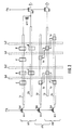
- FIG. 2 In the schematic combined layout circuit diagram shown in FIG. 2 of an exemplary embodiment of the second solution variant of the invention, it is first shown that in each case two adjacent lines including the dummy line according to FIG. 1, the second line lines lz2, ld2 are combined to form the pair line lp can, so that in each of these line pairs instead of the two Evaluate-N transistors the corresponding transistor tez 'is to be provided.
- the line line still remaining for each line and the dummy line is provided with the reference symbol lz throughout in FIG. 2.
- the brackets on the left edge of FIG. 2 indicate which lines of FIG. 1 are represented by the arrangement of FIG. 2.
- FIG. 2 schematically shows the layout in the AND area.
- the horizontal stripes represent interconnects, e.g. made of aluminum, while the vertical, dotted strips also represent interconnects, but preferably made of polycrystalline silicon, and the column lines are.
- corresponding line transistors tz are shown schematically with their layout, namely a transistor between the lower line line lz and the pair line lp or between this and the upper line line lz .
- the drain or source connection of the respective row transistor the channel zone of which is at the intersection of the horizontal transistor part with the respective column line.
- the strongly bordered areas between the mentioned connection area and the channel area are the respective drain or source zones.
- a row transistor tz with its gate is connected to row line ls1, while in the right part of FIG. 2 the lower row transistor tz is connected with its gate to column line ls2.
- zones d are to be provided for each AND cell in the dummy row zd, the maximum number of which is 3n, but there are at least three times as many as in that row of the AND Range, which contains the most line transistors of all these lines.
- Two thirds of zones d are with Row line lz of the dummy row zd and a third contacted with their pair line lp. These zones also have the same area and the same edge length as possible as the zones of the assigned line transistors tz.
- FIG. 2 also shows the N transistor t, which is arranged in the dummy line zd between the line line lz and the pair line lp with its controlled current path and whose gate is connected to the operating voltage source u.
Landscapes
- Physics & Mathematics (AREA)
- Mathematical Physics (AREA)
- Engineering & Computer Science (AREA)
- Computer Hardware Design (AREA)
- Computing Systems (AREA)
- General Engineering & Computer Science (AREA)
- Nonlinear Science (AREA)
- Logic Circuits (AREA)
- Design And Manufacture Of Integrated Circuits (AREA)
Priority Applications (4)
| Application Number | Priority Date | Filing Date | Title |
|---|---|---|---|
| EP88110267A EP0348539A1 (fr) | 1988-06-28 | 1988-06-28 | Réseau logique programmable CMOS |
| US07/366,830 US4990801A (en) | 1988-06-28 | 1989-06-15 | Internal timing circuit for a CMOS programmable logic array |
| CN89104229.6A CN1014853B (zh) | 1988-06-28 | 1989-06-27 | 互补型金属氧化物半导体可编程逻辑阵列 |
| JP1166489A JPH0252525A (ja) | 1988-06-28 | 1989-06-28 | プログラム可能なcmos論理アレイ |
Applications Claiming Priority (1)
| Application Number | Priority Date | Filing Date | Title |
|---|---|---|---|
| EP88110267A EP0348539A1 (fr) | 1988-06-28 | 1988-06-28 | Réseau logique programmable CMOS |
Publications (1)
| Publication Number | Publication Date |
|---|---|
| EP0348539A1 true EP0348539A1 (fr) | 1990-01-03 |
Family
ID=8199082
Family Applications (1)
| Application Number | Title | Priority Date | Filing Date |
|---|---|---|---|
| EP88110267A Withdrawn EP0348539A1 (fr) | 1988-06-28 | 1988-06-28 | Réseau logique programmable CMOS |
Country Status (4)
| Country | Link |
|---|---|
| US (1) | US4990801A (fr) |
| EP (1) | EP0348539A1 (fr) |
| JP (1) | JPH0252525A (fr) |
| CN (1) | CN1014853B (fr) |
Families Citing this family (12)
| Publication number | Priority date | Publication date | Assignee | Title |
|---|---|---|---|---|
| JP2575899B2 (ja) * | 1989-10-26 | 1997-01-29 | 株式会社東芝 | プリチャージ式論理回路 |
| JPH03231515A (ja) * | 1990-02-06 | 1991-10-15 | Mitsubishi Electric Corp | プログラマブル論理装置 |
| US5204555A (en) * | 1990-04-05 | 1993-04-20 | Gazelle Microcircuits, Inc. | Logic array having high frequency internal clocking |
| US5287018A (en) * | 1990-09-25 | 1994-02-15 | Dallas Semiconductor Corporation | Dynamic PLA time circuit |
| US5572715A (en) * | 1991-02-15 | 1996-11-05 | Cypress Semiconductor Corporation | Architecture and circuits for eliminating skews in PLDs |
| US5121005A (en) * | 1991-04-01 | 1992-06-09 | Motorola, Inc. | Programmable logic array with delayed active pull-ups on the column conductors |
| US5221867A (en) * | 1991-10-11 | 1993-06-22 | Intel Corporation | Programmable logic array with internally generated precharge and evaluation timing |
| US5576636A (en) * | 1995-08-15 | 1996-11-19 | Intel Corporation | Low power programmable logic arrays |
| US5646556A (en) * | 1995-11-27 | 1997-07-08 | Advanced Micro Devices, Inc. | Apparatus and method for precharging bus conductors to minimize both drive delay and crosstalk within the bus |
| US5872462A (en) * | 1996-02-20 | 1999-02-16 | International Business Machines Corporation | Programmable logic array and method for its design using a three step approach |
| US7346861B1 (en) * | 2004-12-02 | 2008-03-18 | Altera Corporation | Programmable logic devices with two-phase latch circuitry |
| CN101888240B (zh) * | 2009-05-11 | 2012-10-24 | 复旦大学 | 一种现场可编程逻辑阵列的通用互连盒结构及建模方法 |
Citations (1)
| Publication number | Priority date | Publication date | Assignee | Title |
|---|---|---|---|---|
| EP0178437A1 (fr) * | 1984-09-19 | 1986-04-23 | Siemens Aktiengesellschaft | Circuit programmable réalisé en technique CMOS dynamique |
Family Cites Families (7)
| Publication number | Priority date | Publication date | Assignee | Title |
|---|---|---|---|---|
| US4740721A (en) * | 1985-10-21 | 1988-04-26 | Western Digital Corporation | Programmable logic array with single clock dynamic logic |
| US4675556A (en) * | 1986-06-09 | 1987-06-23 | Intel Corporation | Binomially-encoded finite state machine |
| US4697105A (en) * | 1986-07-23 | 1987-09-29 | American Telephone And Telegraph Company, At&T Bell Laboratories | CMOS programmable logic array |
| IT1195119B (it) * | 1986-08-04 | 1988-10-12 | Cselt Centro Studi Lab Telecom | Perfezionamenti alle schiere logi che programmabili dinamiche a struttura nor nor realizzate in tecnolo gia c mos |
| US4760290A (en) * | 1987-05-21 | 1988-07-26 | Vlsi Technology, Inc. | Synchronous logic array circuit with dummy signal lines for controlling "AND" array output |
| JPH01109922A (ja) * | 1987-10-23 | 1989-04-26 | Mitsubishi Electric Corp | プログラマブルロジツクアレイ |
| US4831285A (en) * | 1988-01-19 | 1989-05-16 | National Semiconductor Corporation | Self precharging static programmable logic array |
-
1988
- 1988-06-28 EP EP88110267A patent/EP0348539A1/fr not_active Withdrawn
-
1989
- 1989-06-15 US US07/366,830 patent/US4990801A/en not_active Expired - Fee Related
- 1989-06-27 CN CN89104229.6A patent/CN1014853B/zh not_active Expired
- 1989-06-28 JP JP1166489A patent/JPH0252525A/ja active Pending
Patent Citations (1)
| Publication number | Priority date | Publication date | Assignee | Title |
|---|---|---|---|---|
| EP0178437A1 (fr) * | 1984-09-19 | 1986-04-23 | Siemens Aktiengesellschaft | Circuit programmable réalisé en technique CMOS dynamique |
Non-Patent Citations (2)
| Title |
|---|
| N.H.E. WESTE et al.: "Principles of CMOS VLSI design", 1985, Seiten 372-373; Addison-Wesley Publishing Co., Reading, Mass., US * |
| PATENT ABSTRACTS OF JAPAN, Band 10, Nr. 283, (E-440)[2339]; & JP-A-61 101 124 (HITACHI MICRO COMPUT ENG LTD) 20-05-1986 * |
Also Published As
| Publication number | Publication date |
|---|---|
| CN1039688A (zh) | 1990-02-14 |
| CN1014853B (zh) | 1991-11-20 |
| JPH0252525A (ja) | 1990-02-22 |
| US4990801A (en) | 1991-02-05 |
Similar Documents
| Publication | Publication Date | Title |
|---|---|---|
| EP0051693B1 (fr) | Mémoire morte électriquement commutable | |
| DE2723821C2 (de) | Programmierbare logische Anordnung | |
| DE2726094C2 (de) | Programmierbare Logik in Matrixanordnung | |
| DE2731442C2 (de) | Speicherschaltung mit Isolierschicht-Feldeffekttransistoren | |
| DE3779705T2 (de) | Integrierte speicherschaltung mit blockadressierung. | |
| DE2018473A1 (de) | Binär logischer Schaltkreis, insbesondere zur Durchführung einer programmierten Fo Igeschaltung | |
| DE102019133640B4 (de) | Bitzelle, die eine bit-schreib-maskierungsfunktion unterstützt | |
| DE2261786C3 (fr) | ||
| DE69221827T2 (de) | Verfahren zum Programmieren einer anwenderprogrammierbaren Gattermatrix | |
| DE2261786B2 (de) | Festwert-Speichereinheit | |
| EP0056434A2 (fr) | Mémoire semiconductrice monolithique intégrée | |
| DE2706807A1 (de) | Einrichtung und verfahren zum verarbeiten von information in form digitaler signale | |
| DE3751607T2 (de) | Stromversorgungsleitungen in einer integrierten Halbleiterschaltung. | |
| EP0078338B1 (fr) | Mémoire TEC | |
| DE4406459A1 (de) | Integrierte Halbleiterschaltungsvorrichtung mit Speicherzellenanordnung | |
| DE2646653A1 (de) | Leseverstaerker fuer statische speichereinrichtung | |
| EP0321589B1 (fr) | Mémoire FIFO numérique | |
| DE2625351A1 (de) | Matrixschaltung und daraus gebildeter dekoder | |
| DE68919155T2 (de) | Halbleiterspeicheranordnung mit verschiedenen Substrat-Vorspannungsschaltungen. | |
| DE2022256C2 (de) | Festwertspeicher- und Decoderanordnung | |
| EP1033753A2 (fr) | Dispositif de mémoire à semiconducteur avec des composants factices dans une région diffusée continue | |
| DE2452319A1 (de) | Decodiererschaltung | |
| DE69125576T2 (de) | Speicheranordnung mit Abtastverstärkern vom Stromspiegeltyp | |
| EP0066050B1 (fr) | Réseau logique programmable à haut degré d'intégration | |
| DE3220205A1 (de) | Elektrische schaltungsanordnung |
Legal Events
| Date | Code | Title | Description |
|---|---|---|---|
| PUAI | Public reference made under article 153(3) epc to a published international application that has entered the european phase |
Free format text: ORIGINAL CODE: 0009012 |
|
| AK | Designated contracting states |
Kind code of ref document: A1 Designated state(s): DE FR NL |
|
| 17P | Request for examination filed |
Effective date: 19900630 |
|
| 17Q | First examination report despatched |
Effective date: 19920211 |
|
| STAA | Information on the status of an ep patent application or granted ep patent |
Free format text: STATUS: THE APPLICATION HAS BEEN WITHDRAWN |
|
| 18W | Application withdrawn |
Withdrawal date: 19920613 |