EP0349302A2 - Méthode et dispositif pour contrôler un téléphone électronique à prépaiment pendant les interruptions de boucle - Google Patents
Méthode et dispositif pour contrôler un téléphone électronique à prépaiment pendant les interruptions de boucle Download PDFInfo
- Publication number
- EP0349302A2 EP0349302A2 EP89306582A EP89306582A EP0349302A2 EP 0349302 A2 EP0349302 A2 EP 0349302A2 EP 89306582 A EP89306582 A EP 89306582A EP 89306582 A EP89306582 A EP 89306582A EP 0349302 A2 EP0349302 A2 EP 0349302A2
- Authority
- EP
- European Patent Office
- Prior art keywords
- open switch
- power
- coin
- switch interval
- occurrence
- Prior art date
- Legal status (The legal status is an assumption and is not a legal conclusion. Google has not performed a legal analysis and makes no representation as to the accuracy of the status listed.)
- Granted
Links
Images


Classifications
-
- H—ELECTRICITY
- H04—ELECTRIC COMMUNICATION TECHNIQUE
- H04M—TELEPHONIC COMMUNICATION
- H04M19/00—Current supply arrangements for telephone systems
-
- H—ELECTRICITY
- H04—ELECTRIC COMMUNICATION TECHNIQUE
- H04M—TELEPHONIC COMMUNICATION
- H04M19/00—Current supply arrangements for telephone systems
- H04M19/08—Current supply arrangements for telephone systems with current supply sources at the substations
-
- H—ELECTRICITY
- H04—ELECTRIC COMMUNICATION TECHNIQUE
- H04M—TELEPHONIC COMMUNICATION
- H04M17/00—Prepayment of wireline communication systems, wireless communication systems or telephone systems
- H04M17/02—Coin-freed or check-freed systems, e.g. mobile- or card-operated phones, public telephones or booths
- H04M17/023—Circuit arrangements
-
- Y—GENERAL TAGGING OF NEW TECHNOLOGICAL DEVELOPMENTS; GENERAL TAGGING OF CROSS-SECTIONAL TECHNOLOGIES SPANNING OVER SEVERAL SECTIONS OF THE IPC; TECHNICAL SUBJECTS COVERED BY FORMER USPC CROSS-REFERENCE ART COLLECTIONS [XRACs] AND DIGESTS
- Y02—TECHNOLOGIES OR APPLICATIONS FOR MITIGATION OR ADAPTATION AGAINST CLIMATE CHANGE
- Y02D—CLIMATE CHANGE MITIGATION TECHNOLOGIES IN INFORMATION AND COMMUNICATION TECHNOLOGIES [ICT], I.E. INFORMATION AND COMMUNICATION TECHNOLOGIES AIMING AT THE REDUCTION OF THEIR OWN ENERGY USE
- Y02D30/00—Reducing energy consumption in communication networks
- Y02D30/70—Reducing energy consumption in communication networks in wireless communication networks
Definitions
- This invention relates to control apparatus for line operated telephones. More particularly, this invention relates to a low power control apparatus for a coin operated telephone which primarily draws its power for operation from the phone lines even though line power is typically removed during a number of events in the course of a typical payphone call.
- Coin operated telephone stations are interfaced with a central office by a two wire loop circuit.
- the central office supplies a very small DC loop current, typically 23 mA minimum, which is available to the coin operated telephone for use as a source of power.
- This source of power is interrupted during a number of events in the course of a typical payphone call.
- open switch intervals vary according to the control switching system in use at the central office. For older switching systems, open switch intervals are typically 350 milliseconds (ms) but under certain conditions can extend up to 600 ms. In fact, under worst case conditions, such intervals have been measured to last as long as 4 seconds.
- off hook operation with an open switch condition occurring only a very small amount of internal battery power is employed for such operations as monitoring the status of significant events during the open switch condition.
- the present invention provides a low power control apparatus for coin operated telephones or any other line powered telephone.
- This low power control utilizes a relatively small battery for a limited range of functions.
- the present control apparatus utilizes solely phone line power to power its various operations even though that line power is subject to interruption as a result of open switch intervals due to central office switching.
- FIG. 1 shows a coin operated phone 2 which is connected to a central office 4 by two wires, the phone lines, which are referred to as the tip 6 and ring 8 lines.
- phone 2 includes a handset 10 having a mouthpiece 11 and an earpiece 12, which are connected by a handle 13.
- the phone 2 also includes a keypad 14, a coin slot 16, and a coin return slot 18.
- the handset 10 sits in a cradle 19 depressing a spring loaded switch 20, the hook switch.
- hook switch 20 and phone 2 are then in their "on hook" position.
- the phone 2 When handset 10 is on hook, the phone 2 draws no power from the tip 6 or ring 8. The phone 2 does, however, perform status monitoring in its standby state using a small amount of power from a relatively small internal battery.
- a customer picks up handset 10 thereby releasing the hook switch 20 from its depressed position.
- the phone 2 enters its off hook state, and begins to draw power from the tip 6 and ring 8 to process the call.
- the customer inserts a sufficient number of coins into the coin slot 16 to cover the cost of the call and dials the number he wishes to call using keypad 14.
- the dialed number is transmitted to central office 4 which connects the call.
- the customer's money is collected by phone 2 when a collect signal from the central office 4 is received. The customer completes his call and then hangs up.
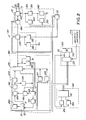
- a line interface circuit 55 comprising a ground lifting relay circuit 160 and an off hook detector circuit 190 connects the tip 6 and ring 8 lines from the central office 4 to a power supply circuit 230.
- the ground lifting relay circuit 160 also serves to selectively connect the tip and ring lines 6 and 8 to a coin totalizer control circuit 350 comprising a totalizer relay circuit 355, a coin supervisor detector circuit 360, a coin relay circuit 365 and a first coin bypass circuit 370.
- the interconnection of a coin acceptor 30 which is responsible for accepting and validating coins deposited in coin slot 16 of FIG. 1 is also represented in FIG. 2.
- the coin acceptor 30 directs accepted coins to a standard coin telephone escrow bucket (not shown). This escrow bucket holds the coins in escrow until completion of the time period for which the coins were deposited and then collects them based on commands from the central office 4 and resulting control signals produced by totalizer control circuit 350.
- Coin acceptor 30 provides output signals to processing element 100 and in return receives operational control inputs from the processing element 100.
- Processing element 100 is shown in FIG. 2 as comprising a real time clock 102, memory 104 and a microcontroller 110.
- power supply circuit 230 that circuit is shown in FIG. 2 as having outputs connected to a gate solenoid power circuit 250, a DC power supply circuit 260, and an audio network 380. More specifically, power supply 230 provides power to a standard DTMF keypad which is presently preferred for use as the keypad 14 of FIG. 1, a DTMF decode circuit 395 and a speech network 390. With the exception of the limited functions powered from battery 511 which is part of a monitor system 510, the power supply circuit 230 in conjunction with control signals from processing element 100 controls the provision of all power for the low power controller 50.
- Power for operating a coin routing gate for controlling the routing of coins within the coin acceptor 30 is provided through power supply 230, to the gate solenoid power supply 250, and from there to the coin routing gate. Power for all the digital electronic components requiring a DC supply is provided through supply 230 to the DC power supply 260.
- the audio network 380 When the audio network 380 is powered up, it provides the phone 2 with the capability of transmitting and receiving speech and audio tone signals. These signals are transmitted and received as AC voltages on the tip 6 and ring 8 which are offset by the DC voltage applied by the central office 4.
- the processing element 100 through its single microcontroller 110 controls all the operations of phone 2 including audio network 380, coin acceptor 30, and power supply 230. Microcontroller 110 also records the status of the phone 2 and has the capability of initiating communications during the standby mode if that status warrants it.
- Audio network 380 comprises a large number of interconnected blocks under the control of microcontroller 110. More specifically, the speech network 390 is connected to the DTMF decode circuit 395 and the DTMF keypad 14. Further, the speech network 390 is also connected to a coin tone generator 320, a DTMF generator 321, an audio balance circuit 480, a first switch 405, and notch filter circuit 470. The DTMF decode circuit 395, the coin tone generator 320 and the DTMF generator 321 are in turn connected to a modem circuit 400. Modem circuit 400 is also connected to the first switch 405 and a second switch 420. The notch filter circuit 470 is connected through a low pass filter (LPF) circuit 415 to the second switch 420.
- LPF low pass filter
- the second switch 420 is also connected to a microphone in the mouthpiece 11 which is part of the handset 10.
- First switch 405 is connected to a level adjust circuit 410 which is in turn connected to an ear piece 12 which is part of the handset 10.
- Handset 10 is further connected to a handset detector circuit 430.
- the DTMF decode circuit 395, the coin tone generator 320, the DTMF generator 321, the modem 400, the first and second switches 405 and 420, the level adjust 410, the handset detector 430, and the notch filter circuit 470 are all further connected to microcontroller 110 and the monitor system 510.
- monitor system 510 monitors the status of the phone 2.
- monitor system 510 draws its power from power supply 230 which is energized by power from the tip 6 and ring 8 lines when the handset 10 if off hook. Consequently, normal operational power for monitor circuit 520 is provided from the phone line.
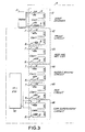
- FIG. 3 of the drawings the phone 2 is again shown as in FIG. 1 connected to the central office 4 by tip and ring lines 6 and 8 respectively.
- the central office 4 is shown in greater detail in order to illustrate how open switch intervals occur and why no or insufficient power is available to phone 2 on the tip and ring lines 6 and 8 during OSI.
- the central office 4 includes a switching control 40, such as the No. 1 ESS (Electronic Switching System) manufactured by Western Electric.
- Switching control 40 controllably switches the tip and ring lines 6 and 8 so that a plurality of different function control supply modules can be connected one at a time to the tip and ring lines 6 and 8 at the appropriate times.
- Each supply module connects a bank of batteries V BATT through its own voltage adjusting circuitry to the tip and ring lines when that module is switched into operation by switching control 40.
- FIG. 1 ESS Electronic Switching System
- FIG. 3 shows a DTMF decoder supply module 41, a trunk supply module 42, a high and wet list supply module 43, an audible ringing supply module 44, an off hook ringing supply module 45 and a coin supervisory supply module 46 which are all controllably switched by switching control 40 at appropriate times.
- Each of the supply modules 41-46 includes a respective pair of switches 41a, 41b; 42a, 42b; 43a, 43b; 44a, 44b; 45a, 45b; and 46a, 46b. These switches are controlled by the switching control 40 to control which one of the supply modules 41-46 is connected to the tip and ring lines 6 and 8. Consequently, the DC voltage supplied to the phone 2 is controlled by whatever supply module is connected at that time.
- open switch intervals may occur as follows. After the receiver 13 is taken off the hook, an open switch interval will follow. Then, the DTMF decoder supply module 41 is switched in by the switching control 40 in order to allow the customer to dial the digits of the number he desires to reach. An open switch interval follows the disconnection of the DTMF decoder supply module 41 until the coin supervisory supply module 46 is switched in to determine if an adequate amount of money has been inserted. Another open switch interval also precedes the switching of the audible ringing supply module 44 which causes the call to ring through. An open switch interval precedes connection of the trunk supply module 42 which allows voice communication once the called party has answered the call. Further open switch intervals precede collect and refund coin signals supplied by the coin supervisory control module 46. Finally, the user hangs up at the completion of the call.
- a number of events are monitored even in the on hook condition through the use of battery operated electronic latches. Specifically, the state of the hook switch 20, as well as the occurrences of a collect or a refund operation are monitored. These conditions are particularly important since if they occur during an open switch interval, phone 2 is expected to reset differently than if they had not occurred.
- open switch intervals are detected by a line monitoring circuit 60 shown in FIG 6.
- This circuit 60 gives the microcontroller 110 warning that the power has been removed and a minimum amount of time (typically about 200 ms for a control circuit in accordance with the preferred embodiment of the present invention) remains to prepare for power down.
- This 200 ms power down time is a result of a relatively small capacitor (1000 uF) in the power supply circuit 230.
- the system then proceeds to save its present status along with the state of the key hardware outputs in nonvolatile memory 104.
- the microcontroller 110 comes out of its reset condition and recreates its pre-OSI status by recalling the stored status information from memory.
- battery powered latches 70 and 80 are checked to determine if the switch hook 20 returned to the on hook position or if the collect or refund signals indicate that either of these conditions has occurred during the OSI. The appropriate actions are then taken by microcontroller 110.
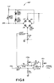
- the hook switch latch circuit 72 is part of battery powered latch 70 which includes two latch circuits.
- the central part of latch 70 is latch U16, which is a CMOS circuit supplied by a battery V batt .
- the latch U16 also serves to monitor a coin box switch which is not shown.
- the coin box switch monitors the coin box, and its details are well known and not part of the present invention.
- latch U16 In its ready state, the voltages at the HYST2 and SET2 inputs of latch U16 are determined by resistors R53, R54 and R55. Latch U16 operates in a manner to switch its output OUT2 low (approximately 0 volts) if the HYST2 input is below the SET2 input. The output OUT2 remains low until the SET2 input is raised to the battery level V batt .
- the switch hook 20 In the event the switch hook 20 is changed to the on hook condition, the signal on the Hook Switch line goes low thus pulling the HYST2 input low as that input is connected through resistor R60 to the Hook Switch line. This low at the HYST2 input causes the OUT2 output of latch U16 to go low thus storing an indication that the switch 20 has been closed. In other words, latch U16 stores the information that the phone has been hung up during an OSI. When power is returned after the OSI, the output OUT2 is monitored to determine if the switch hook 20 was on hook or not during the open switch interval. If it was, then the microcontroller 110 causes the STATE RESET 1 line to go low, turning "on" transistor Q5 through base resistor R4.
- FIG. 5 shows a refund latch circuit 82 which works exactly as the hook switch circuit 72 described above except that it is triggered by a refund signal indicative of the occurrence of a refund operation.
- FIG. 5 also shows a collect circuit 84 which works similar to the hook switch and refund latches 72 and 82 except that the HYST1, SET1 signals for collect circuit 84 are the reverse sense as the HYST2 and SET2 signals. That is, the output OUT1 signal is brought low when HYST1 is brought to essentially V batt and the OUT1 signal is reset when the SET1 signal is brought essentially to 0 volts (low).
- FIGS. 4 and 5 While several preferred battery-powered latch circuits are shown in FIGS. 4 and 5 and described above, it should be recognized that additional such latches may be designed to monitor any other condition deemed particularly worthy of monitoring during an open switch interval.
- FIG. 6 illustrates a presently preferred line power monitoring circuit 60.
- the current through the line (tip to ring) is measured through a resistor R29. If the current falls below a predetermined threshold determined by resistors Rb, Rc, Rd and Re, then the output of comparator U28 changes level indicating the power loss condition.
- the output signal from comparator U28 is connected to the microcontroller 110 which responds by initiating its power down sequence.
- FIG. 7 The presently preferred power down sequence is shown in FIG. 7 in a Program Design Language description which is written for the 80C31 microprocessor. Actual software used to implement the logic of FIG. 7 is attached as Appendix A.
Landscapes
- Engineering & Computer Science (AREA)
- Signal Processing (AREA)
- Computer Networks & Wireless Communication (AREA)
- Computer Security & Cryptography (AREA)
- Prepayment Telephone Systems (AREA)
- Devices For Supply Of Signal Current (AREA)
- Telephone Function (AREA)
- Mobile Radio Communication Systems (AREA)
- Keying Circuit Devices (AREA)
- Interconnected Communication Systems, Intercoms, And Interphones (AREA)
Applications Claiming Priority (2)
| Application Number | Priority Date | Filing Date | Title |
|---|---|---|---|
| US213223 | 1988-06-28 | ||
| US07/213,223 US4979208A (en) | 1988-06-29 | 1988-06-29 | Method and apparatus for electronic payphone open switch interval management |
Publications (3)
| Publication Number | Publication Date |
|---|---|
| EP0349302A2 true EP0349302A2 (fr) | 1990-01-03 |
| EP0349302A3 EP0349302A3 (fr) | 1991-03-27 |
| EP0349302B1 EP0349302B1 (fr) | 1995-08-16 |
Family
ID=22794225
Family Applications (1)
| Application Number | Title | Priority Date | Filing Date |
|---|---|---|---|
| EP89306582A Expired - Lifetime EP0349302B1 (fr) | 1988-06-28 | 1989-06-28 | Méthode et dispositif pour contrôler un téléphone électronique à prépaiment pendant les interruptions de boucle |
Country Status (15)
| Country | Link |
|---|---|
| US (1) | US4979208A (fr) |
| EP (1) | EP0349302B1 (fr) |
| JP (1) | JP2940969B2 (fr) |
| KR (1) | KR900701116A (fr) |
| CN (2) | CN1038907A (fr) |
| AT (1) | ATE126643T1 (fr) |
| BR (1) | BR8907499A (fr) |
| CA (1) | CA1312970C (fr) |
| DE (1) | DE68923832T2 (fr) |
| DK (1) | DK307090D0 (fr) |
| ES (1) | ES2076213T3 (fr) |
| HU (1) | HUT61144A (fr) |
| MX (1) | MX164475B (fr) |
| NO (1) | NO905604L (fr) |
| WO (1) | WO1990000333A1 (fr) |
Cited By (2)
| Publication number | Priority date | Publication date | Assignee | Title |
|---|---|---|---|---|
| WO1993018608A1 (fr) * | 1992-03-12 | 1993-09-16 | Landis & Gyr Business Support Ag | Procede et dispositif permettant la reduction de consommation de puissance dans un telephone publique |
| DE4219416A1 (de) * | 1992-06-13 | 1993-12-16 | Grundig Emv | Verfahren und Schaltungsanordnung zur Begrenzung der Verbindungsgebühren für Teilnehmereinrichtungen |
Families Citing this family (8)
| Publication number | Priority date | Publication date | Assignee | Title |
|---|---|---|---|---|
| EP0556278B2 (fr) * | 1990-11-07 | 2002-05-22 | Mars Incorporated | Procede et appareil destines a un distributeur automatique fonctionnant avec piles et de faible puissance |
| DE4301530C1 (de) * | 1993-01-21 | 1994-06-30 | Nat Rejectors Gmbh | Induktiver Einschaltsensor für batteriebetriebene Münzprüfer |
| US5818916A (en) * | 1993-10-19 | 1998-10-06 | Technology Service Group | Method and apparatus for preventing return dial tone fraud in a cellular paystation |
| FR2725333B1 (fr) * | 1994-09-30 | 1996-12-13 | Ind Tech Res Inst | Procede et appareil pour la gestion de la puissance et la commande d'un reseau telephonique rnis |
| US5896446A (en) * | 1996-07-29 | 1999-04-20 | Mars Incorporated | Coin operated telephone auditor |
| US6320945B1 (en) * | 1997-06-05 | 2001-11-20 | Ronald J. Honick | Line-powered pay telephone |
| US5956323A (en) * | 1997-07-30 | 1999-09-21 | Nokia High Speed Access Products Inc. | Power conservation for pots and modulated data transmission |
| GB2348730B (en) | 1999-04-07 | 2003-02-19 | Mars Inc | Currency handling apparatus |
Family Cites Families (18)
| Publication number | Priority date | Publication date | Assignee | Title |
|---|---|---|---|---|
| US3428751A (en) * | 1966-01-28 | 1969-02-18 | Bell Telephone Labor Inc | Coin telephone antifraud circuit |
| US4039768A (en) * | 1976-05-26 | 1977-08-02 | Maley James B O | Pay telephone station monitor system |
| US4074079A (en) * | 1976-06-02 | 1978-02-14 | Bell Telephone Laboratories, Incorporated | Coin telephone antifraud system |
| US4031325A (en) * | 1976-06-21 | 1977-06-21 | Bell Telephone Laboratories, Incorporated | Called party fraud prevention in an automated coin system |
| US4046962A (en) * | 1976-09-03 | 1977-09-06 | Bell Telephone Laboratories, Incorporated | Called party fraud detection in an automated coin system |
| US4326103A (en) * | 1980-06-02 | 1982-04-20 | Gte Automatic Electric Labs Inc. | Coin telephone monitor circuit |
| US4361731A (en) * | 1981-02-13 | 1982-11-30 | Bell Telephone Laboratories, Incorporated | Coin telephone control circuit |
| US4674114A (en) * | 1983-12-30 | 1987-06-16 | At&T Technologies Inc. And At&T Bell Laboratories | Fraud prevention in an electronic coin telephone set |
| US4567325A (en) * | 1983-12-30 | 1986-01-28 | At&T Technologies Inc. | Controller for a coin telephone set |
| US4625078A (en) * | 1983-12-30 | 1986-11-25 | At&T Technologies Inc. | Fraud prevention in an electronic coin telephone set |
| JPS61205065A (ja) * | 1985-03-08 | 1986-09-11 | Tamura Electric Works Ltd | 公衆電話機 |
| JPS62295555A (ja) * | 1986-06-16 | 1987-12-22 | Tamura Electric Works Ltd | 公衆電話機 |
| JPS63103311A (ja) * | 1986-10-20 | 1988-05-09 | Victor Co Of Japan Ltd | マイクロコンピユ−タシステムの停電時の処理方法 |
| US4742536A (en) * | 1986-10-24 | 1988-05-03 | Energy Innovations, Inc. | Telephone monitor circuit and method |
| US4759054A (en) * | 1986-12-22 | 1988-07-19 | Protel, Inc. | Toll telephone system and method for maintaining or initiating loop current after resuming on-hook condition |
| US4782516A (en) * | 1987-06-25 | 1988-11-01 | AT&T Information Systems Inc. American Telephone and Telegraph Company | Fraud prevention in a public telephone station |
| US4794642A (en) * | 1987-09-24 | 1988-12-27 | American Telephone And Telegraph Company, At&T Bell Laboratories | Call screening in a public telephone station |
| US4926458A (en) * | 1988-05-26 | 1990-05-15 | Mars Incorporated | Low power control apparatus for a coin operated telephone |
-
1988
- 1988-06-29 US US07/213,223 patent/US4979208A/en not_active Expired - Fee Related
-
1989
- 1989-06-21 CA CA000603460A patent/CA1312970C/fr not_active Expired - Fee Related
- 1989-06-23 KR KR1019890702484A patent/KR900701116A/ko not_active Ceased
- 1989-06-23 JP JP1507419A patent/JP2940969B2/ja not_active Expired - Lifetime
- 1989-06-23 WO PCT/US1989/002772 patent/WO1990000333A1/fr not_active Ceased
- 1989-06-23 BR BR898907499A patent/BR8907499A/pt unknown
- 1989-06-23 HU HU894139A patent/HUT61144A/hu unknown
- 1989-06-26 CN CN89104445A patent/CN1038907A/zh active Pending
- 1989-06-27 MX MX8916617A patent/MX164475B/es unknown
- 1989-06-28 ES ES89306582T patent/ES2076213T3/es not_active Expired - Lifetime
- 1989-06-28 EP EP89306582A patent/EP0349302B1/fr not_active Expired - Lifetime
- 1989-06-28 DE DE68923832T patent/DE68923832T2/de not_active Expired - Fee Related
- 1989-06-28 AT AT89306582T patent/ATE126643T1/de not_active IP Right Cessation
-
1990
- 1990-12-27 NO NO90905604A patent/NO905604L/no unknown
- 1990-12-28 DK DK307090A patent/DK307090D0/da not_active Application Discontinuation
-
1992
- 1992-05-18 CN CN92104031A patent/CN1067144A/zh active Pending
Cited By (2)
| Publication number | Priority date | Publication date | Assignee | Title |
|---|---|---|---|---|
| WO1993018608A1 (fr) * | 1992-03-12 | 1993-09-16 | Landis & Gyr Business Support Ag | Procede et dispositif permettant la reduction de consommation de puissance dans un telephone publique |
| DE4219416A1 (de) * | 1992-06-13 | 1993-12-16 | Grundig Emv | Verfahren und Schaltungsanordnung zur Begrenzung der Verbindungsgebühren für Teilnehmereinrichtungen |
Also Published As
| Publication number | Publication date |
|---|---|
| US4979208A (en) | 1990-12-18 |
| JP2940969B2 (ja) | 1999-08-25 |
| DK307090A (da) | 1990-12-28 |
| EP0349302A3 (fr) | 1991-03-27 |
| BR8907499A (pt) | 1991-05-28 |
| NO905604D0 (no) | 1990-12-27 |
| CN1038907A (zh) | 1990-01-17 |
| JPH03501796A (ja) | 1991-04-18 |
| CN1067144A (zh) | 1992-12-16 |
| NO905604L (no) | 1990-12-27 |
| DK307090D0 (da) | 1990-12-28 |
| CA1312970C (fr) | 1993-01-19 |
| ATE126643T1 (de) | 1995-09-15 |
| MX164475B (es) | 1992-08-19 |
| ES2076213T3 (es) | 1995-11-01 |
| HUT61144A (en) | 1992-11-30 |
| KR900701116A (ko) | 1990-08-17 |
| DE68923832D1 (de) | 1995-09-21 |
| DE68923832T2 (de) | 1996-04-18 |
| EP0349302B1 (fr) | 1995-08-16 |
| WO1990000333A1 (fr) | 1990-01-11 |
Similar Documents
| Publication | Publication Date | Title |
|---|---|---|
| US5046085A (en) | Interfacing system for an international-type pay-telephone | |
| CA1312971C (fr) | Dispositif de commande a faible puissance pour telephone a perception automatique | |
| US5311582A (en) | Integrated cocot and regulated paystation telephone system | |
| EP0349302B1 (fr) | Méthode et dispositif pour contrôler un téléphone électronique à prépaiment pendant les interruptions de boucle | |
| US4028494A (en) | Escrow telephone coin collection circuit and method | |
| US5907606A (en) | Telephone-line powered coin telephone chassis | |
| SE518141C2 (sv) | Förfarande för exekvering av en automatisk uppringning | |
| US4768222A (en) | Control and surveillance system for prepayment public telephone apparatus | |
| US3760101A (en) | Coin telephone circuit | |
| US4942604A (en) | Line power control circuit for pay station telephone | |
| US4811386A (en) | Called party response detecting apparatus | |
| AU620765B2 (en) | Method and apparatus for electronic payphone open switch interval management | |
| US3890468A (en) | Circuit arrangement for ground start coin operated telephones | |
| JPH0427748B2 (fr) | ||
| JPH0753326Y2 (ja) | テレビ及び電話の課金装置 | |
| JPS61206355A (ja) | 選択着信方式 | |
| JPH0137897B2 (fr) | ||
| JP2970156B2 (ja) | 公衆電話機 | |
| JPH0246142Y2 (fr) | ||
| JP2684280B2 (ja) | 公衆電話機 | |
| JP2861587B2 (ja) | ダイヤルイン処理回路 | |
| JPS58157249A (ja) | 公衆電話機の金庫情報送信方式 | |
| JP3367032B2 (ja) | 料金徴収式電話機 | |
| JPH07131560A (ja) | 不正通話防止装置 | |
| JPH03235573A (ja) | 課金装置を有する電話機 |
Legal Events
| Date | Code | Title | Description |
|---|---|---|---|
| PUAI | Public reference made under article 153(3) epc to a published international application that has entered the european phase |
Free format text: ORIGINAL CODE: 0009012 |
|
| AK | Designated contracting states |
Kind code of ref document: A2 Designated state(s): AT BE CH DE ES FR GB GR IT LI LU NL SE |
|
| 17P | Request for examination filed |
Effective date: 19901211 |
|
| PUAL | Search report despatched |
Free format text: ORIGINAL CODE: 0009013 |
|
| AK | Designated contracting states |
Kind code of ref document: A3 Designated state(s): AT BE CH DE ES FR GB GR IT LI LU NL SE |
|
| K1C1 | Correction of patent application (title page) published |
Effective date: 19900103 |
|
| 17Q | First examination report despatched |
Effective date: 19930428 |
|
| GRAA | (expected) grant |
Free format text: ORIGINAL CODE: 0009210 |
|
| AK | Designated contracting states |
Kind code of ref document: B1 Designated state(s): AT BE CH DE ES FR GB GR IT LI LU NL SE |
|
| PG25 | Lapsed in a contracting state [announced via postgrant information from national office to epo] |
Ref country code: LI Effective date: 19950816 Ref country code: IT Free format text: LAPSE BECAUSE OF FAILURE TO SUBMIT A TRANSLATION OF THE DESCRIPTION OR TO PAY THE FEE WITHIN THE PRE;WARNING: LAPSES OF ITALIAN PATENTS WITH EFFECTIVE DATE BEFORE 2007 MAY HAVE OCCURRED AT ANY TIME BEFORE 2007. THE CORRECT EFFECTIVE DATE MAY BE DIFFERENT FROM THE ONE RECORDED.SCRIBED TIME-LIMIT Effective date: 19950816 Ref country code: NL Free format text: LAPSE BECAUSE OF FAILURE TO SUBMIT A TRANSLATION OF THE DESCRIPTION OR TO PAY THE FEE WITHIN THE PRESCRIBED TIME-LIMIT Effective date: 19950816 Ref country code: BE Effective date: 19950816 Ref country code: CH Effective date: 19950816 Ref country code: AT Effective date: 19950816 Ref country code: GR Free format text: LAPSE BECAUSE OF FAILURE TO SUBMIT A TRANSLATION OF THE DESCRIPTION OR TO PAY THE FEE WITHIN THE PRESCRIBED TIME-LIMIT Effective date: 19950816 |
|
| REF | Corresponds to: |
Ref document number: 126643 Country of ref document: AT Date of ref document: 19950915 Kind code of ref document: T |
|
| REF | Corresponds to: |
Ref document number: 68923832 Country of ref document: DE Date of ref document: 19950921 |
|
| ET | Fr: translation filed | ||
| REG | Reference to a national code |
Ref country code: ES Ref legal event code: FG2A Ref document number: 2076213 Country of ref document: ES Kind code of ref document: T3 |
|
| PG25 | Lapsed in a contracting state [announced via postgrant information from national office to epo] |
Ref country code: SE Effective date: 19951116 |
|
| NLV1 | Nl: lapsed or annulled due to failure to fulfill the requirements of art. 29p and 29m of the patents act | ||
| PLBE | No opposition filed within time limit |
Free format text: ORIGINAL CODE: 0009261 |
|
| STAA | Information on the status of an ep patent application or granted ep patent |
Free format text: STATUS: NO OPPOSITION FILED WITHIN TIME LIMIT |
|
| PG25 | Lapsed in a contracting state [announced via postgrant information from national office to epo] |
Ref country code: LU Free format text: LAPSE BECAUSE OF NON-PAYMENT OF DUE FEES Effective date: 19960630 |
|
| 26N | No opposition filed | ||
| PGFP | Annual fee paid to national office [announced via postgrant information from national office to epo] |
Ref country code: FR Payment date: 20010611 Year of fee payment: 13 |
|
| PGFP | Annual fee paid to national office [announced via postgrant information from national office to epo] |
Ref country code: DE Payment date: 20010618 Year of fee payment: 13 |
|
| PGFP | Annual fee paid to national office [announced via postgrant information from national office to epo] |
Ref country code: GB Payment date: 20010627 Year of fee payment: 13 |
|
| PGFP | Annual fee paid to national office [announced via postgrant information from national office to epo] |
Ref country code: ES Payment date: 20010629 Year of fee payment: 13 |
|
| REG | Reference to a national code |
Ref country code: GB Ref legal event code: IF02 |
|
| PG25 | Lapsed in a contracting state [announced via postgrant information from national office to epo] |
Ref country code: GB Free format text: LAPSE BECAUSE OF NON-PAYMENT OF DUE FEES Effective date: 20020628 |
|
| PG25 | Lapsed in a contracting state [announced via postgrant information from national office to epo] |
Ref country code: ES Free format text: LAPSE BECAUSE OF NON-PAYMENT OF DUE FEES Effective date: 20020629 |
|
| PG25 | Lapsed in a contracting state [announced via postgrant information from national office to epo] |
Ref country code: DE Free format text: LAPSE BECAUSE OF NON-PAYMENT OF DUE FEES Effective date: 20030101 |
|
| GBPC | Gb: european patent ceased through non-payment of renewal fee |
Effective date: 20020628 |
|
| PG25 | Lapsed in a contracting state [announced via postgrant information from national office to epo] |
Ref country code: FR Free format text: LAPSE BECAUSE OF NON-PAYMENT OF DUE FEES Effective date: 20030228 |
|
| REG | Reference to a national code |
Ref country code: FR Ref legal event code: ST |
|
| REG | Reference to a national code |
Ref country code: ES Ref legal event code: FD2A Effective date: 20030711 |