EP0349741A2 - Dispositif semi-conducteur avec interaction optique - Google Patents
Dispositif semi-conducteur avec interaction optique Download PDFInfo
- Publication number
- EP0349741A2 EP0349741A2 EP89108863A EP89108863A EP0349741A2 EP 0349741 A2 EP0349741 A2 EP 0349741A2 EP 89108863 A EP89108863 A EP 89108863A EP 89108863 A EP89108863 A EP 89108863A EP 0349741 A2 EP0349741 A2 EP 0349741A2
- Authority
- EP
- European Patent Office
- Prior art keywords
- substrate
- region
- charge carrier
- carrier region
- optical
- Prior art date
- Legal status (The legal status is an assumption and is not a legal conclusion. Google has not performed a legal analysis and makes no representation as to the accuracy of the status listed.)
- Withdrawn
Links
- 239000004065 semiconductor Substances 0.000 title claims abstract description 22
- 230000003287 optical effect Effects 0.000 title claims description 39
- 230000003993 interaction Effects 0.000 title abstract description 12
- 239000000758 substrate Substances 0.000 claims abstract description 34
- 239000002800 charge carrier Substances 0.000 claims abstract description 32
- 238000000034 method Methods 0.000 claims description 8
- 230000005693 optoelectronics Effects 0.000 claims description 8
- 230000010287 polarization Effects 0.000 claims description 6
- 238000010521 absorption reaction Methods 0.000 claims description 5
- 229920000136 polysorbate Polymers 0.000 claims 1
- 239000000523 sample Substances 0.000 abstract description 21
- 238000010586 diagram Methods 0.000 description 5
- 229910001218 Gallium arsenide Inorganic materials 0.000 description 3
- XUIMIQQOPSSXEZ-UHFFFAOYSA-N Silicon Chemical compound [Si] XUIMIQQOPSSXEZ-UHFFFAOYSA-N 0.000 description 2
- JNDMLEXHDPKVFC-UHFFFAOYSA-N aluminum;oxygen(2-);yttrium(3+) Chemical compound [O-2].[O-2].[O-2].[Al+3].[Y+3] JNDMLEXHDPKVFC-UHFFFAOYSA-N 0.000 description 2
- 230000000694 effects Effects 0.000 description 2
- 238000004519 manufacturing process Methods 0.000 description 2
- 239000000463 material Substances 0.000 description 2
- 229910052710 silicon Inorganic materials 0.000 description 2
- 239000010703 silicon Substances 0.000 description 2
- 229910019901 yttrium aluminum garnet Inorganic materials 0.000 description 2
- 238000003491 array Methods 0.000 description 1
- 239000013078 crystal Substances 0.000 description 1
- 230000008021 deposition Effects 0.000 description 1
- 238000005530 etching Methods 0.000 description 1
- 238000012986 modification Methods 0.000 description 1
- 230000004048 modification Effects 0.000 description 1
- 238000005070 sampling Methods 0.000 description 1
- 239000007787 solid Substances 0.000 description 1
- 238000000992 sputter etching Methods 0.000 description 1
Images


Classifications
-
- H—ELECTRICITY
- H10—SEMICONDUCTOR DEVICES; ELECTRIC SOLID-STATE DEVICES NOT OTHERWISE PROVIDED FOR
- H10F—INORGANIC SEMICONDUCTOR DEVICES SENSITIVE TO INFRARED RADIATION, LIGHT, ELECTROMAGNETIC RADIATION OF SHORTER WAVELENGTH OR CORPUSCULAR RADIATION
- H10F30/00—Individual radiation-sensitive semiconductor devices in which radiation controls the flow of current through the devices, e.g. photodetectors
- H10F30/20—Individual radiation-sensitive semiconductor devices in which radiation controls the flow of current through the devices, e.g. photodetectors the devices having potential barriers, e.g. phototransistors
- H10F30/21—Individual radiation-sensitive semiconductor devices in which radiation controls the flow of current through the devices, e.g. photodetectors the devices having potential barriers, e.g. phototransistors the devices being sensitive to infrared, visible or ultraviolet radiation
- H10F30/28—Individual radiation-sensitive semiconductor devices in which radiation controls the flow of current through the devices, e.g. photodetectors the devices having potential barriers, e.g. phototransistors the devices being sensitive to infrared, visible or ultraviolet radiation the devices being characterised by field-effect operation, e.g. junction field-effect phototransistors
- H10F30/285—Individual radiation-sensitive semiconductor devices in which radiation controls the flow of current through the devices, e.g. photodetectors the devices having potential barriers, e.g. phototransistors the devices being sensitive to infrared, visible or ultraviolet radiation the devices being characterised by field-effect operation, e.g. junction field-effect phototransistors the devices having PN homojunction gates
- H10F30/2863—Field-effect phototransistors having PN homojunction gates
-
- G—PHYSICS
- G11—INFORMATION STORAGE
- G11C—STATIC STORES
- G11C11/00—Digital stores characterised by the use of particular electric or magnetic storage elements; Storage elements therefor
- G11C11/21—Digital stores characterised by the use of particular electric or magnetic storage elements; Storage elements therefor using electric elements
- G11C11/34—Digital stores characterised by the use of particular electric or magnetic storage elements; Storage elements therefor using electric elements using semiconductor devices
- G11C11/40—Digital stores characterised by the use of particular electric or magnetic storage elements; Storage elements therefor using electric elements using semiconductor devices using transistors
- G11C11/41—Digital stores characterised by the use of particular electric or magnetic storage elements; Storage elements therefor using electric elements using semiconductor devices using transistors forming static cells with positive feedback, i.e. cells not needing refreshing or charge regeneration, e.g. bistable multivibrator or Schmitt trigger
- G11C11/412—Digital stores characterised by the use of particular electric or magnetic storage elements; Storage elements therefor using electric elements using semiconductor devices using transistors forming static cells with positive feedback, i.e. cells not needing refreshing or charge regeneration, e.g. bistable multivibrator or Schmitt trigger using field-effect transistors only
-
- G—PHYSICS
- G11—INFORMATION STORAGE
- G11C—STATIC STORES
- G11C11/00—Digital stores characterised by the use of particular electric or magnetic storage elements; Storage elements therefor
- G11C11/21—Digital stores characterised by the use of particular electric or magnetic storage elements; Storage elements therefor using electric elements
- G11C11/42—Digital stores characterised by the use of particular electric or magnetic storage elements; Storage elements therefor using electric elements using opto-electronic devices, i.e. light-emitting and photoelectric devices electrically- or optically- coupled or feedback-coupled
-
- H—ELECTRICITY
- H10—SEMICONDUCTOR DEVICES; ELECTRIC SOLID-STATE DEVICES NOT OTHERWISE PROVIDED FOR
- H10F—INORGANIC SEMICONDUCTOR DEVICES SENSITIVE TO INFRARED RADIATION, LIGHT, ELECTROMAGNETIC RADIATION OF SHORTER WAVELENGTH OR CORPUSCULAR RADIATION
- H10F77/00—Constructional details of devices covered by this subclass
- H10F77/40—Optical elements or arrangements
- H10F77/407—Optical elements or arrangements indirectly associated with the devices
-
- H—ELECTRICITY
- H10—SEMICONDUCTOR DEVICES; ELECTRIC SOLID-STATE DEVICES NOT OTHERWISE PROVIDED FOR
- H10F—INORGANIC SEMICONDUCTOR DEVICES SENSITIVE TO INFRARED RADIATION, LIGHT, ELECTROMAGNETIC RADIATION OF SHORTER WAVELENGTH OR CORPUSCULAR RADIATION
- H10F77/00—Constructional details of devices covered by this subclass
- H10F77/40—Optical elements or arrangements
- H10F77/413—Optical elements or arrangements directly associated or integrated with the devices, e.g. back reflectors
Definitions
- the invention is related to semiconductor devices in which a lengthened optical interaction beam path is provided to enhance interaction of a probe beam and charge carriers present in a carrier region of the devices.
- a plurality of optical memory elements may be interconnected to form a random access memory array as described in the application of Aaron Falk entitled “Opto-Electronic Memory Device” filed concurrently herewith (Attorney Docket No. 87FAL411DAB) and incorporated herein by reference.
- the probe beam In conventional semiconductor devices, the probe beam must enter the substrate of the device in a substantially perpendicular manner in order to probe the charge carrier region.
- the charge carrier region usually consists of a long thin region parallel to the surface of the substrate.
- the probe beam passes through the shortest dimension of the charge carrier region limiting the interaction path length of the probe beam and the charge carriers.
- the object of the present invention is to provide a semiconductor device in which a long interaction path length is provided for a non-invasive probe beam.
- mirrors are etched in the surface of the semiconductor substrate which are used to reflect the probe beam along the longest dimension of the charge carrier region. Interaction between the probe beam and the charge carriers present in the region is thereby enhanced.
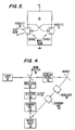
- a simplified cross-sectional view is provided of a conventional FET semiconductor device having a substrate 10, a source region 12, a carrier region 14, and a drain region 16.
- Corresponding source, gate, and drain electrodes 18,20 and 22 are formed on the top surface of the substrate 10.
- the probe beam enters the bottom surface of the substrate 10 and is reflected from the gate electrode 20.
- the probe beam i.e. read beam
- the probe beam passes through the depth dimension of the carrier region 14, which is shorter than the length of the carrier region, thereby limiting interaction of the probe beam and any charge carriers present in the carrier region 14.
- mirror surfaces 24 and 26 are formed in the surface of the substrate 10′.
- Conventional ion milling or etching techniques are employed to form the mirror surfaces 24 and 26 in substrate 10′ so that the optical path of a probe beam applied to the device passes through the longest dimension of the charge carrier region 14′.
- the longest dimension is the length of the carrier region which is parallel to the top surface of the device.
- the mirror surfaces 24 and 26 may be formed in the substrate at various times in the production process, but are preferably formed after the deposition of the source region 12′ and drain region 16′.
- the interaction length of the device shown in Fig. 2 therefore, is effectively extended over the conventional FET in which the read beam would enter the substrate perpendicular to the path of the charge carriers. It is clear that the optical path through the charge carrier region is advantageously selected to be at least approximately parallel to the top surface of the semiconductor device and traverses a distance through the charge carrier region which is substantially greater than the depth of the charge carrier region.
- a semiconductor device may be employed in optical memory systems.
- an optical flip-flop 28 (shown in Fig. 3) composed of two photo-FETs 30 and 32 that utilize the mirror surfaces 24 and 26 illustrated in Fig. 2, can be employed as an elemental memory device in a fully optical memory.
- One of the photo-FETs 30 is probed by a read beam to determine if charge is flowing through the device. For example, in order to "store” a logic "1", a write beam activates photo-FET 30 causing current to flow through that photo-FET. Changes to the phase and/or polarization of the reflected read beam are then used to determine that photo-FET 30 is "ON" thereby indicating a "1" has been stored.
- the write light is directed to photo-FET 32 causing photo-FET 30 to be switched "OFF".
- a memory array consisting of a plurality of the elemental memory devices illustrated in Fig. 3 can be formed using conventional solid state device fabrication techniques to form a fully optical random access memory.
- a single yttrium aluminum garnet (YAG) laser 32 is utilized to provide a both the read beam and write beam used to address an optical random access memory array 34 made in GaAs.
- a beam splitter 36 splits the beam from the laser 32 into a read beam and a write beam which are supplied to modulators 38 and 40, respectively.
- the modulators 38 and 40 selectively block the read and write beams to effect "on-off" control of the beams.
- the frequency of the write beam is first doubled by a doubling crystal 42 before being provided to the modulator 40.
- the wavelength of the write beam is preferably about 532nm and the wavelength of the read beam is preferably about 1064nm.
- Scanning units 44 and 46 then independently scan the modulated read and write beams across the memory array to selectively address the elemental memory devices for reading and writing, respectively.
- a detector unit 48 analyzes phase and/or polarization changes in the reflected read beam in order to determine the charge density present in the area probed by the read beam.
- the detector unit 48 detects the index of refraction change resulting from charge modulation or through the electro-optic effect by employing a high resolution interferometer, noninvasive technique, such as disclosed in the above referenced paper by Heinrich et al entitled, "Noninvasive Sheet Charge Density Probe for Integrated Silicon Devices" the contents of which are incorporated herein by reference.
- Detector 48 is illustrated in Figure 4.
- the read beam from modulator 38 is passed through a polarizing beam splitter 50 and then through a birefringent beam splitter 52 which produces two beams of orthogonal polarization.
- An objective lens 54 focuses the two beams, which are deflected by the scanner unit 44, onto the memory array 34.
- One beam passes through the active area of the memory array to be probed while the second beam is reflected from a metallized area of the memory array 34 serving as a reference point.
- the two beams are reflected back along the same optical path and are recombined into a single beam by the birefringent beam splitter 52.
- the polarizing beam splitter 50 and a lens 55 direct the reflected light to a photodetector circuit 56 which produces an intensity modulated interference product.
- the output of the photodetector circuit 56 provides an intensity modulated electrical signal which is linear with respect to charge density.
- the invention may also be employed in the parallel memory addressing array as disclosed in the above-referenced Falk application.
Landscapes
- Engineering & Computer Science (AREA)
- Microelectronics & Electronic Packaging (AREA)
- Computer Hardware Design (AREA)
- Semiconductor Memories (AREA)
- Testing Or Measuring Of Semiconductors Or The Like (AREA)
Applications Claiming Priority (2)
| Application Number | Priority Date | Filing Date | Title |
|---|---|---|---|
| US203726 | 1988-06-07 | ||
| US07/203,726 US5150182A (en) | 1988-06-07 | 1988-06-07 | Semiconductor device enhanced for optical interaction |
Publications (2)
| Publication Number | Publication Date |
|---|---|
| EP0349741A2 true EP0349741A2 (fr) | 1990-01-10 |
| EP0349741A3 EP0349741A3 (fr) | 1990-04-25 |
Family
ID=22755076
Family Applications (1)
| Application Number | Title | Priority Date | Filing Date |
|---|---|---|---|
| EP89108863A Withdrawn EP0349741A3 (fr) | 1988-06-07 | 1989-05-17 | Dispositif semi-conducteur avec interaction optique |
Country Status (5)
| Country | Link |
|---|---|
| US (1) | US5150182A (fr) |
| EP (1) | EP0349741A3 (fr) |
| JP (1) | JPH0284750A (fr) |
| KR (1) | KR900000997A (fr) |
| AU (1) | AU3611689A (fr) |
Families Citing this family (5)
| Publication number | Priority date | Publication date | Assignee | Title |
|---|---|---|---|---|
| US5663075A (en) * | 1994-07-14 | 1997-09-02 | The United States Of America As Represented By The Secretary Of The Air Force | Method of fabricating backside illuminated FET optical receiver with gallium arsenide species |
| US6393169B1 (en) * | 1997-12-19 | 2002-05-21 | Intel Corporation | Method and apparatus for providing optical interconnection |
| US6462814B1 (en) | 2000-03-15 | 2002-10-08 | Schlumberger Technologies, Inc. | Beam delivery and imaging for optical probing of a device operating under electrical test |
| US7806365B2 (en) * | 2006-07-05 | 2010-10-05 | The Boeing Company | Long endurance hydrogen powered vehicle |
| JP2015064413A (ja) * | 2013-09-24 | 2015-04-09 | 富士通株式会社 | 光半導体素子とその製造方法 |
Family Cites Families (9)
| Publication number | Priority date | Publication date | Assignee | Title |
|---|---|---|---|---|
| US3210622A (en) * | 1959-09-11 | 1965-10-05 | Philips Corp | Photo-transistor |
| FR2057341A5 (fr) * | 1969-08-12 | 1971-05-21 | Comp Generale Electricite | |
| DE2407523A1 (de) * | 1974-02-16 | 1975-08-21 | Messerschmitt Boelkow Blohm | Photoempfindliches verstaerkungselement |
| US3996492A (en) * | 1975-05-28 | 1976-12-07 | International Business Machines Corporation | Two-dimensional integrated injection laser array |
| JPS53121494A (en) * | 1978-03-10 | 1978-10-23 | Agency Of Ind Science & Technol | Photo electric converter having sensitivity to light of long wave lenght |
| DE3016498A1 (de) * | 1980-04-29 | 1981-11-05 | Siemens AG, 1000 Berlin und 8000 München | Lichtempfindliche halbleiterbauelemente |
| JPS5724573A (en) * | 1980-07-21 | 1982-02-09 | Sumitomo Electric Ind Ltd | Semiconductor light-receiver element |
| JPS6088482A (ja) * | 1983-10-20 | 1985-05-18 | Fuji Electric Corp Res & Dev Ltd | 光電変換装置 |
| DE3429812C1 (de) * | 1984-08-14 | 1986-04-10 | Messerschmitt-Bölkow-Blohm GmbH, 8012 Ottobrunn | Monolithischer Bildaufnehmer |
-
1988
- 1988-06-07 US US07/203,726 patent/US5150182A/en not_active Expired - Fee Related
-
1989
- 1989-05-17 EP EP89108863A patent/EP0349741A3/fr not_active Withdrawn
- 1989-06-05 KR KR1019890007695A patent/KR900000997A/ko not_active Withdrawn
- 1989-06-06 AU AU36116/89A patent/AU3611689A/en not_active Abandoned
- 1989-06-07 JP JP1145039A patent/JPH0284750A/ja active Pending
Also Published As
| Publication number | Publication date |
|---|---|
| AU3611689A (en) | 1989-12-14 |
| KR900000997A (ko) | 1990-01-31 |
| JPH0284750A (ja) | 1990-03-26 |
| EP0349741A3 (fr) | 1990-04-25 |
| US5150182A (en) | 1992-09-22 |
Similar Documents
| Publication | Publication Date | Title |
|---|---|---|
| KR100504135B1 (ko) | 적외선 레이저 프로브를 이용하여 집적회로 내의 전압을직접 측정하기 위한 방법 및 장치 | |
| Smits et al. | Design considerations for a semipermanent optical memory | |
| US5150182A (en) | Semiconductor device enhanced for optical interaction | |
| US4789964A (en) | Optoelectronic dynamic random access memory system | |
| JP3072814B2 (ja) | 電気光学プローブ及びその製造方法 | |
| US5055770A (en) | Method and apparatus for detecting voltage | |
| US6967765B2 (en) | Active optical system for changing the wavelength of an image | |
| US3812477A (en) | Method for superresolution in an optical memory | |
| US4873485A (en) | Electro-optic signal measurement | |
| US4877312A (en) | Bistable optical photorefractive crystal device | |
| EP0345494A2 (fr) | Dispositif de mémoire opto-électronique | |
| US5086409A (en) | Recording and/or reproducing method of bloch line memory | |
| US5822471A (en) | Differential optical modulator | |
| US3427456A (en) | Laser images formed by matric control | |
| US5923182A (en) | Ferroelectric optical computing device with low optical power non-destructive read-out | |
| US3515887A (en) | Optical scanner including at least one gunn-effect oscillator element | |
| JP3576681B2 (ja) | 光記憶装置 | |
| JPH02284131A (ja) | 光学ビーム間の相関用装置 | |
| US3573469A (en) | Optically controlled phase adjustment for electrical signals | |
| US3576547A (en) | Interferometric readout of electric fields | |
| GB1328282A (en) | Electronic-optical memory system | |
| JPH02150776A (ja) | 電圧検出装置 | |
| JPS6120931A (ja) | 光制御装置 | |
| McCormick et al. | Optical and mechanical issues in free-space digital optical logic systems | |
| KR100245829B1 (ko) | 광장치 |
Legal Events
| Date | Code | Title | Description |
|---|---|---|---|
| PUAI | Public reference made under article 153(3) epc to a published international application that has entered the european phase |
Free format text: ORIGINAL CODE: 0009012 |
|
| AK | Designated contracting states |
Kind code of ref document: A2 Designated state(s): DE FR GB SE |
|
| PUAL | Search report despatched |
Free format text: ORIGINAL CODE: 0009013 |
|
| AK | Designated contracting states |
Kind code of ref document: A3 Designated state(s): DE FR GB SE |
|
| 17P | Request for examination filed |
Effective date: 19901008 |
|
| STAA | Information on the status of an ep patent application or granted ep patent |
Free format text: STATUS: THE APPLICATION IS DEEMED TO BE WITHDRAWN |
|
| 18D | Application deemed to be withdrawn |
Effective date: 19911203 |