EP0350663A2 - Montage de circuit pour la démodulation d'une sous-porteuse - Google Patents
Montage de circuit pour la démodulation d'une sous-porteuse Download PDFInfo
- Publication number
- EP0350663A2 EP0350663A2 EP89111145A EP89111145A EP0350663A2 EP 0350663 A2 EP0350663 A2 EP 0350663A2 EP 89111145 A EP89111145 A EP 89111145A EP 89111145 A EP89111145 A EP 89111145A EP 0350663 A2 EP0350663 A2 EP 0350663A2
- Authority
- EP
- European Patent Office
- Prior art keywords
- mixed
- frequency
- circuit arrangement
- signals
- signal
- Prior art date
- Legal status (The legal status is an assumption and is not a legal conclusion. Google has not performed a legal analysis and makes no representation as to the accuracy of the status listed.)
- Granted
Links
- 238000001914 filtration Methods 0.000 claims abstract description 3
- 238000006243 chemical reaction Methods 0.000 claims abstract 2
- 238000005070 sampling Methods 0.000 description 9
- 239000000654 additive Substances 0.000 description 3
- 230000000996 additive effect Effects 0.000 description 3
- 230000036039 immunity Effects 0.000 description 2
- 230000033228 biological regulation Effects 0.000 description 1
- 239000000969 carrier Substances 0.000 description 1
- 238000009795 derivation Methods 0.000 description 1
- 238000011161 development Methods 0.000 description 1
- 230000018109 developmental process Effects 0.000 description 1
- 238000010586 diagram Methods 0.000 description 1
- 239000000203 mixture Substances 0.000 description 1
- 230000005236 sound signal Effects 0.000 description 1
- 230000003595 spectral effect Effects 0.000 description 1
- 230000001629 suppression Effects 0.000 description 1
Images
Classifications
-
- H—ELECTRICITY
- H03—ELECTRONIC CIRCUITRY
- H03D—DEMODULATION OR TRANSFERENCE OF MODULATION FROM ONE CARRIER TO ANOTHER
- H03D1/00—Demodulation of amplitude-modulated oscillations
- H03D1/22—Homodyne or synchrodyne circuits
- H03D1/2245—Homodyne or synchrodyne circuits using two quadrature channels
- H03D1/2254—Homodyne or synchrodyne circuits using two quadrature channels and a phase locked loop
-
- H—ELECTRICITY
- H03—ELECTRONIC CIRCUITRY
- H03B—GENERATION OF OSCILLATIONS, DIRECTLY OR BY FREQUENCY-CHANGING, BY CIRCUITS EMPLOYING ACTIVE ELEMENTS WHICH OPERATE IN A NON-SWITCHING MANNER; GENERATION OF NOISE BY SUCH CIRCUITS
- H03B28/00—Generation of oscillations by methods not covered by groups H03B5/00 - H03B27/00, including modification of the waveform to produce sinusoidal oscillations
-
- H—ELECTRICITY
- H03—ELECTRONIC CIRCUITRY
- H03D—DEMODULATION OR TRANSFERENCE OF MODULATION FROM ONE CARRIER TO ANOTHER
- H03D7/00—Transference of modulation from one carrier to another, e.g. frequency-changing
- H03D7/16—Multiple-frequency-changing
- H03D7/165—Multiple-frequency-changing at least two frequency changers being located in different paths, e.g. in two paths with carriers in quadrature
Definitions
- the invention relates to a circuit arrangement according to the type of the main claim.
- an additive error occurs at the output.
- This error can occur in particular in the case of a useful signal, such as, for example, the subcarrier of the traffic radio system and the radio data system (RDS).
- a useful signal such as, for example, the subcarrier of the traffic radio system and the radio data system (RDS).
- the object of the invention is to provide a circuit arrangement for demodulating an auxiliary carrier in which digital further processing of the useful signal is possible without an additive error occurring. Furthermore, since stronger interference signals such as audio signals and the stereopilot sound occur in connection with the subcarrier in addition, interference immunity of the circuit, in particular suppression of image frequencies, is required.
- circuit arrangement according to the invention with the characterizing features of the main claim has the advantage that digital further processing of the useful signal is possible, practically no additive error occurs and that there is a sufficiently high level of interference immunity.
- circuit arrangement according to the invention can be implemented with little effort and is suitable for an integrated circuit.
- circuit arrangement according to the invention places only low demands on the speed of the analog / digital converter, simple, easily integrable analog / digital converters (for example delta converters or sigma-delta converters) can be used which have a high dynamic range in the low frequency range allow signals to be converted.
- analog / digital converters for example delta converters or sigma-delta converters
- two mixed signals with a phase difference of 90 o are generated.
- a derivation of both quadrature components is possible in a simple manner by scanning the mixed products four times.
- the invention also includes the generation of more than two mixed signals with corresponding phase differences and a more frequent sampling of the mixed products. In the case of an even number of mixed signals, sampling values for both quadrature components are readily available.
- quadrature components can also be derived in the case of an odd number of mixed signals, one being able to be obtained directly and the other by interpolation between two samples.
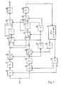
- the circuit arrangement according to FIG. 1 is supplied with the signal to be demodulated at 11. It follows the relationship A (t) * sin ( ⁇ t + ⁇ ).
- a (t) is the modulation signal, while ⁇ and ⁇ stand, as usual, for the angular frequency and the phase position of the carrier.
- the RDS and traffic radio subcarrier has a frequency of 57 kHz.
- the mixers 12, 13 are each supplied with a mixed signal, the frequency of which is 61.75 kHz. It is generated in a digitally controllable oscillator 14 and a subsequent frequency divider 31 in two phase positions different from one another by 90 ° by frequency division of a signal with four times the frequency of the mixed signals.
- Subsequent low-pass filters 15, 16 suppress spectral components above the useful frequency range.
- the output signals of the low-pass filters 15, 16 then result in A (t) * cos (( ⁇ 0 - ⁇ 57) t + ⁇ ) or A (t) * sin (( ⁇ 0 - ⁇ 57) t + ⁇ ).
- the mixture does not yet convert the modulation signal A (t) into the baseband, but rather only modulated carriers with a frequency of 4.75 kHz are created.
- Both signals which are called intermediate frequency signals in the following, are each fed to an analog / digital converter 17, 18, a clock frequency of 19 KHz being provided by dividing the frequency of the oscillator 14 by 13 with the aid of a Frequency divider 19 is generated and samples the intermediate frequency signals four times per period.
- the outputs of the analog / digital converters 17, 18 are followed by two channels I and II, each of which is controlled by a controllable changeover switch 20, 21, a signal inverter 22, 23, a further controllable changeover switch 24, 25 and a low-pass filter 26, 27 be formed.
- the output signal of the low-pass filter 26 can be taken from an output 28, while the output signal of the low-pass filter 27 is used in the exemplary embodiment shown to control the digitally controllable oscillator 14.
- the switches 20, 21, 24, 25 are controlled via two further frequency dividers 29, 30 in such a way that in channel I a sampling takes place at 0 o and 180 o in relation to a period of the intermediate frequency signal, while in channel II at 90 o and 270 o is scanned. Every second sample value is inverted with the aid of the circuits 22, 23, so that demodulation into the baseband takes place. After filtering out carrier residues with the aid of low-pass filters 26, 27, the demodulated signals are available.
- the signal at the output 28 corresponds to the cosine component of the modulation signal, while a sine component is available at the output of the low-pass filter 27, which is used for regulation in the exemplary embodiment shown.
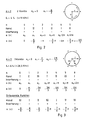
- n means the ordinal number of the respective scan, + or - whether a signal inversion takes place and ⁇ (n) the respective angle of the scan in general form and with 0 as the initial value.
- ⁇ (n) the respective angle of the scan in general form and with 0 as the initial value.
- the positions of the changeover switch are marked with the values for n, in which the respective position is assumed.
- the table according to FIG. 2 shows that the samples are taken alternately from channel I and channel II. Two successive samples are forwarded with the same sign, so that every second half-wave of the intermediate frequency signal is inverted. Through this inversion, any offset error that may be present during the scanning of one of the channels I or II is alternately inverted and not inverted. The offset error is thus converted into a frequency of 4.75 kHz, which is suppressed by the subsequent low-pass filter 26 or 27.
- n 0, 3, 4, 7, 8, etc.
- FIG. 2 or as a graphic representation of the sampling times 0, 1, 2, 3 and the intermediate frequency signals, wherein the signal of the channel I that of channel II advances 90 o.
- the sampling frequency fs 19 kHz.
- the sampling frequency means the frequency with which the output signals of the analog / digital converters or downstream filters are processed further.
- the table according to FIG. 3 explains an exemplary embodiment with three channels.
- the phase differences are each ⁇ / 3.
- the sampling frequency fs is six times the intermediate frequency, which corresponds to a sampling frequency of 28.5 kHz at an intermediate frequency of 4.75 kHz.
- the intermediate frequency signals are shown in the pie chart of FIG. 3, which also shows the six sampling times 0 to 5.
- the respective channel to be scanned, the sign and the angle of the scanning for both orthogonal components are listed for the scanning times.
Landscapes
- Engineering & Computer Science (AREA)
- Power Engineering (AREA)
- Digital Transmission Methods That Use Modulated Carrier Waves (AREA)
- Circuits Of Receivers In General (AREA)
- Stereo-Broadcasting Methods (AREA)
- Superheterodyne Receivers (AREA)
Applications Claiming Priority (2)
| Application Number | Priority Date | Filing Date | Title |
|---|---|---|---|
| DE3823552A DE3823552C2 (de) | 1988-07-12 | 1988-07-12 | Schaltungsanordnung zur Demodulation eines Hilfsträgers |
| DE3823552 | 1988-07-12 |
Publications (3)
| Publication Number | Publication Date |
|---|---|
| EP0350663A2 true EP0350663A2 (fr) | 1990-01-17 |
| EP0350663A3 EP0350663A3 (fr) | 1990-11-28 |
| EP0350663B1 EP0350663B1 (fr) | 1996-09-11 |
Family
ID=6358481
Family Applications (1)
| Application Number | Title | Priority Date | Filing Date |
|---|---|---|---|
| EP89111145A Expired - Lifetime EP0350663B1 (fr) | 1988-07-12 | 1989-06-20 | Montage de circuit pour la démodulation d'une sous-porteuse |
Country Status (4)
| Country | Link |
|---|---|
| EP (1) | EP0350663B1 (fr) |
| AT (1) | ATE142825T1 (fr) |
| DE (2) | DE3823552C2 (fr) |
| ES (1) | ES2091755T3 (fr) |
Cited By (2)
| Publication number | Priority date | Publication date | Assignee | Title |
|---|---|---|---|---|
| EP0545245A3 (en) * | 1991-12-05 | 1993-11-03 | Blaupunkt Werke Gmbh | Digital oscillator |
| EP1239616A3 (fr) * | 2001-03-10 | 2004-01-28 | Harman/Becker Automotive Systems (Becker Division) GmbH | Procédé et Dispositif pour la Démodulation d'un Signal RDS |
Families Citing this family (1)
| Publication number | Priority date | Publication date | Assignee | Title |
|---|---|---|---|---|
| DE10317598A1 (de) | 2003-04-16 | 2004-11-25 | Infineon Technologies Ag | Integrierter Transceiverschaltkreis |
Family Cites Families (5)
| Publication number | Priority date | Publication date | Assignee | Title |
|---|---|---|---|---|
| DE3114063A1 (de) * | 1981-04-07 | 1982-10-21 | Licentia Patent-Verwaltungs-Gmbh, 6000 Frankfurt | Empfangssystem |
| FR2560688B1 (fr) * | 1984-03-02 | 1987-07-17 | Thomson Csf | Dispositif de traitement du signal de reception radar a frequence intermediaire et radar comportant un tel dispositif |
| DE3516282A1 (de) * | 1985-05-07 | 1986-11-13 | Blaupunkt Werke Gmbh | Digitaler demodulator |
| DE3627007A1 (de) * | 1986-08-09 | 1988-02-18 | Blaupunkt Werke Gmbh | Demodulator zur demodulation von eingangssignalen |
| JPS6387052A (ja) * | 1986-09-30 | 1988-04-18 | Pioneer Electronic Corp | Fm多重放送受信機におけるデ−タ復調回路 |
-
1988
- 1988-07-12 DE DE3823552A patent/DE3823552C2/de not_active Expired - Fee Related
-
1989
- 1989-06-20 EP EP89111145A patent/EP0350663B1/fr not_active Expired - Lifetime
- 1989-06-20 ES ES89111145T patent/ES2091755T3/es not_active Expired - Lifetime
- 1989-06-20 DE DE58909726T patent/DE58909726D1/de not_active Expired - Fee Related
- 1989-06-20 AT AT89111145T patent/ATE142825T1/de not_active IP Right Cessation
Cited By (3)
| Publication number | Priority date | Publication date | Assignee | Title |
|---|---|---|---|---|
| EP0545245A3 (en) * | 1991-12-05 | 1993-11-03 | Blaupunkt Werke Gmbh | Digital oscillator |
| US5355393A (en) * | 1991-12-05 | 1994-10-11 | Blaupunkt-Werke Gmbh | Digital oscillator for carrier frequency synchronization |
| EP1239616A3 (fr) * | 2001-03-10 | 2004-01-28 | Harman/Becker Automotive Systems (Becker Division) GmbH | Procédé et Dispositif pour la Démodulation d'un Signal RDS |
Also Published As
| Publication number | Publication date |
|---|---|
| ES2091755T3 (es) | 1996-11-16 |
| DE58909726D1 (de) | 1996-10-17 |
| DE3823552C2 (de) | 1995-08-24 |
| EP0350663A3 (fr) | 1990-11-28 |
| EP0350663B1 (fr) | 1996-09-11 |
| ATE142825T1 (de) | 1996-09-15 |
| DE3823552A1 (de) | 1990-01-18 |
Similar Documents
| Publication | Publication Date | Title |
|---|---|---|
| DE3888336T2 (de) | Einseitenbandsignal-Generatoranordnung. | |
| DE69107247T2 (de) | Elektronische Anordnung zum Empfangen eines modulierten Trägersignals. | |
| EP0308520B1 (fr) | Démodulateur numérique | |
| DE3439893A1 (de) | Signalgenerator | |
| DE1616439B1 (de) | Verfahren und Schaltungsanordnungen zur Signalumwandlung | |
| WO1986005594A1 (fr) | Circuit d'obtention d'une valeur moyenne | |
| EP0200977B1 (fr) | Démodulateur numérique | |
| EP0080157A2 (fr) | Procédé et montage pour la démodulation de signaux modulés en fréquence à partir de valeurs échantillonnées | |
| DE69027889T2 (de) | Modulator | |
| DE3823552C2 (de) | Schaltungsanordnung zur Demodulation eines Hilfsträgers | |
| DE3433592C2 (fr) | ||
| EP3624334A1 (fr) | Dispositif de conversion d'un signal d'entrée analogique en un signal de sortie numérique | |
| DE3240565A1 (de) | Direktmischender synchronempfaenger | |
| EP0755125B1 (fr) | Procédé pour la réduction des postes supplémentaires de réception dans des récepteurs homodynes avec la fréquence porteuse variable en temps | |
| DE3733967C2 (fr) | ||
| DE2627586A1 (de) | Verfahren und schaltungsanordnung zur multiplikation von elektrischen signalen | |
| EP0356555B1 (fr) | Procédé et montage de circuit pour déterminer la présence ou non d'au moins une fréquence d'une valeur connue dans un signal d'entrée composé de plusieurs fréquences | |
| DE69205188T2 (de) | Verfahren zum Reduzieren des Einflusses von Verzerrungsprodukten. | |
| DE3233829A1 (de) | Verfahren zur demodulation amplitudenmodilierter eingangssignale und schaltungsanordnung hierfuer | |
| DE3435032C2 (fr) | ||
| DE4241965C1 (de) | Verfahren zur Demodulation von frequenzmodulierten Signalen | |
| DE3428318C2 (fr) | ||
| DE2407678C3 (de) | Schaltungsanordnung zur Digitalisierung eines Drehwinkel &phgr | |
| DE69231173T2 (de) | Demodulatorschaltung für MSK-Signale | |
| EP0472024A2 (fr) | Système de radar à impulsions |
Legal Events
| Date | Code | Title | Description |
|---|---|---|---|
| PUAI | Public reference made under article 153(3) epc to a published international application that has entered the european phase |
Free format text: ORIGINAL CODE: 0009012 |
|
| AK | Designated contracting states |
Kind code of ref document: A2 Designated state(s): AT CH DE ES FR GB IT LI SE |
|
| PUAL | Search report despatched |
Free format text: ORIGINAL CODE: 0009013 |
|
| AK | Designated contracting states |
Kind code of ref document: A3 Designated state(s): AT CH DE ES FR GB IT LI SE |
|
| 17P | Request for examination filed |
Effective date: 19901018 |
|
| 17Q | First examination report despatched |
Effective date: 19930329 |
|
| GRAH | Despatch of communication of intention to grant a patent |
Free format text: ORIGINAL CODE: EPIDOS IGRA |
|
| GRAH | Despatch of communication of intention to grant a patent |
Free format text: ORIGINAL CODE: EPIDOS IGRA |
|
| GRAA | (expected) grant |
Free format text: ORIGINAL CODE: 0009210 |
|
| AK | Designated contracting states |
Kind code of ref document: B1 Designated state(s): AT CH DE ES FR GB IT LI SE |
|
| REF | Corresponds to: |
Ref document number: 142825 Country of ref document: AT Date of ref document: 19960915 Kind code of ref document: T |
|
| REG | Reference to a national code |
Ref country code: CH Ref legal event code: NV Representative=s name: SCINTILLA AG, DIREKTION |
|
| REF | Corresponds to: |
Ref document number: 58909726 Country of ref document: DE Date of ref document: 19961017 |
|
| ET | Fr: translation filed | ||
| REG | Reference to a national code |
Ref country code: ES Ref legal event code: FG2A Ref document number: 2091755 Country of ref document: ES Kind code of ref document: T3 |
|
| ITF | It: translation for a ep patent filed | ||
| GBT | Gb: translation of ep patent filed (gb section 77(6)(a)/1977) |
Effective date: 19961113 |
|
| PLBE | No opposition filed within time limit |
Free format text: ORIGINAL CODE: 0009261 |
|
| STAA | Information on the status of an ep patent application or granted ep patent |
Free format text: STATUS: NO OPPOSITION FILED WITHIN TIME LIMIT |
|
| 26N | No opposition filed | ||
| EUG | Se: european patent has lapsed | ||
| REG | Reference to a national code |
Ref country code: GB Ref legal event code: IF02 |
|
| PGFP | Annual fee paid to national office [announced via postgrant information from national office to epo] |
Ref country code: GB Payment date: 20060626 Year of fee payment: 18 |
|
| PGFP | Annual fee paid to national office [announced via postgrant information from national office to epo] |
Ref country code: SE Payment date: 20060627 Year of fee payment: 18 Ref country code: CH Payment date: 20060627 Year of fee payment: 18 |
|
| PGFP | Annual fee paid to national office [announced via postgrant information from national office to epo] |
Ref country code: ES Payment date: 20060628 Year of fee payment: 18 |
|
| PGFP | Annual fee paid to national office [announced via postgrant information from national office to epo] |
Ref country code: AT Payment date: 20070622 Year of fee payment: 19 |
|
| PGFP | Annual fee paid to national office [announced via postgrant information from national office to epo] |
Ref country code: DE Payment date: 20070828 Year of fee payment: 19 |
|
| PGFP | Annual fee paid to national office [announced via postgrant information from national office to epo] |
Ref country code: IT Payment date: 20070627 Year of fee payment: 19 |
|
| REG | Reference to a national code |
Ref country code: CH Ref legal event code: PL |
|
| EUG | Se: european patent has lapsed | ||
| GBPC | Gb: european patent ceased through non-payment of renewal fee |
Effective date: 20070620 |
|
| PG25 | Lapsed in a contracting state [announced via postgrant information from national office to epo] |
Ref country code: CH Free format text: LAPSE BECAUSE OF NON-PAYMENT OF DUE FEES Effective date: 20070630 Ref country code: LI Free format text: LAPSE BECAUSE OF NON-PAYMENT OF DUE FEES Effective date: 20070630 |
|
| PGFP | Annual fee paid to national office [announced via postgrant information from national office to epo] |
Ref country code: FR Payment date: 20070619 Year of fee payment: 19 |
|
| PG25 | Lapsed in a contracting state [announced via postgrant information from national office to epo] |
Ref country code: GB Free format text: LAPSE BECAUSE OF NON-PAYMENT OF DUE FEES Effective date: 20070620 |
|
| PG25 | Lapsed in a contracting state [announced via postgrant information from national office to epo] |
Ref country code: SE Free format text: LAPSE BECAUSE OF NON-PAYMENT OF DUE FEES Effective date: 20070621 |
|
| REG | Reference to a national code |
Ref country code: ES Ref legal event code: FD2A Effective date: 20070621 |
|
| PG25 | Lapsed in a contracting state [announced via postgrant information from national office to epo] |
Ref country code: ES Free format text: LAPSE BECAUSE OF NON-PAYMENT OF DUE FEES Effective date: 20070621 |
|
| REG | Reference to a national code |
Ref country code: FR Ref legal event code: ST Effective date: 20090228 |
|
| PG25 | Lapsed in a contracting state [announced via postgrant information from national office to epo] |
Ref country code: AT Free format text: LAPSE BECAUSE OF NON-PAYMENT OF DUE FEES Effective date: 20080620 Ref country code: DE Free format text: LAPSE BECAUSE OF NON-PAYMENT OF DUE FEES Effective date: 20090101 |
|
| PG25 | Lapsed in a contracting state [announced via postgrant information from national office to epo] |
Ref country code: FR Free format text: LAPSE BECAUSE OF NON-PAYMENT OF DUE FEES Effective date: 20080630 Ref country code: IT Free format text: LAPSE BECAUSE OF NON-PAYMENT OF DUE FEES Effective date: 20080620 |