EP0351602A2 - Empaquetage céramique pour semi-conducteur comprenant une configuration contre les craquements - Google Patents
Empaquetage céramique pour semi-conducteur comprenant une configuration contre les craquements Download PDFInfo
- Publication number
- EP0351602A2 EP0351602A2 EP89111822A EP89111822A EP0351602A2 EP 0351602 A2 EP0351602 A2 EP 0351602A2 EP 89111822 A EP89111822 A EP 89111822A EP 89111822 A EP89111822 A EP 89111822A EP 0351602 A2 EP0351602 A2 EP 0351602A2
- Authority
- EP
- European Patent Office
- Prior art keywords
- ceramic
- metal
- semiconductor package
- patterns
- layer
- Prior art date
- Legal status (The legal status is an assumption and is not a legal conclusion. Google has not performed a legal analysis and makes no representation as to the accuracy of the status listed.)
- Granted
Links
Images

Classifications
-
- H—ELECTRICITY
- H10—SEMICONDUCTOR DEVICES; ELECTRIC SOLID-STATE DEVICES NOT OTHERWISE PROVIDED FOR
- H10W—GENERIC PACKAGES, INTERCONNECTIONS, CONNECTORS OR OTHER CONSTRUCTIONAL DETAILS OF DEVICES COVERED BY CLASS H10
- H10W42/00—Arrangements for protection of devices
- H10W42/121—Arrangements for protection of devices protecting against mechanical damage
-
- H—ELECTRICITY
- H05—ELECTRIC TECHNIQUES NOT OTHERWISE PROVIDED FOR
- H05K—PRINTED CIRCUITS; CASINGS OR CONSTRUCTIONAL DETAILS OF ELECTRIC APPARATUS; MANUFACTURE OF ASSEMBLAGES OF ELECTRICAL COMPONENTS
- H05K1/00—Printed circuits
- H05K1/02—Details
- H05K1/0271—Arrangements for reducing stress or warp in rigid printed circuit boards, e.g. caused by loads, vibrations or differences in thermal expansion
-
- H—ELECTRICITY
- H10—SEMICONDUCTOR DEVICES; ELECTRIC SOLID-STATE DEVICES NOT OTHERWISE PROVIDED FOR
- H10W—GENERIC PACKAGES, INTERCONNECTIONS, CONNECTORS OR OTHER CONSTRUCTIONAL DETAILS OF DEVICES COVERED BY CLASS H10
- H10W70/00—Package substrates; Interposers; Redistribution layers [RDL]
- H10W70/60—Insulating or insulated package substrates; Interposers; Redistribution layers
- H10W70/62—Insulating or insulated package substrates; Interposers; Redistribution layers characterised by their interconnections
- H10W70/65—Shapes or dispositions of interconnections
-
- H—ELECTRICITY
- H05—ELECTRIC TECHNIQUES NOT OTHERWISE PROVIDED FOR
- H05K—PRINTED CIRCUITS; CASINGS OR CONSTRUCTIONAL DETAILS OF ELECTRIC APPARATUS; MANUFACTURE OF ASSEMBLAGES OF ELECTRICAL COMPONENTS
- H05K1/00—Printed circuits
- H05K1/02—Details
- H05K1/03—Use of materials for the substrate
- H05K1/0306—Inorganic insulating substrates, e.g. ceramic, glass
-
- H—ELECTRICITY
- H05—ELECTRIC TECHNIQUES NOT OTHERWISE PROVIDED FOR
- H05K—PRINTED CIRCUITS; CASINGS OR CONSTRUCTIONAL DETAILS OF ELECTRIC APPARATUS; MANUFACTURE OF ASSEMBLAGES OF ELECTRICAL COMPONENTS
- H05K2201/00—Indexing scheme relating to printed circuits covered by H05K1/00
- H05K2201/09—Shape and layout
- H05K2201/09145—Edge details
-
- H—ELECTRICITY
- H05—ELECTRIC TECHNIQUES NOT OTHERWISE PROVIDED FOR
- H05K—PRINTED CIRCUITS; CASINGS OR CONSTRUCTIONAL DETAILS OF ELECTRIC APPARATUS; MANUFACTURE OF ASSEMBLAGES OF ELECTRICAL COMPONENTS
- H05K2201/00—Indexing scheme relating to printed circuits covered by H05K1/00
- H05K2201/09—Shape and layout
- H05K2201/09209—Shape and layout details of conductors
- H05K2201/09654—Shape and layout details of conductors covering at least two types of conductors provided for in H05K2201/09218 - H05K2201/095
- H05K2201/09781—Dummy conductors, i.e. not used for normal transport of current; Dummy electrodes of components
-
- H—ELECTRICITY
- H05—ELECTRIC TECHNIQUES NOT OTHERWISE PROVIDED FOR
- H05K—PRINTED CIRCUITS; CASINGS OR CONSTRUCTIONAL DETAILS OF ELECTRIC APPARATUS; MANUFACTURE OF ASSEMBLAGES OF ELECTRICAL COMPONENTS
- H05K2201/00—Indexing scheme relating to printed circuits covered by H05K1/00
- H05K2201/20—Details of printed circuits not provided for in H05K2201/01 - H05K2201/10
- H05K2201/2009—Reinforced areas, e.g. for a specific part of a flexible printed circuit
Definitions
- This invention relates, in general, to semiconductor packages, and more particularly to a ceramic semiconductor package having metal crack arrestor patterns strategically disposed therein.
- Ceramics are especially useful in relatively large packages such as those used in pin grid arrays, leadless chip carriers, dual-in-line side brazed packages and the like. These ceramic packages may be comprised of a single layer of ceramic material or multiple layers of ceramic material that are bonded together. Generally, the ceramic layers are fabricated in a predetermined manner so that metal interconnect lines may be formed thereon. Tungsten alloys and other like metals are commonly used to form the interconnect lines. Ceramic semiconductor packages having multiple bonded ceramic layers as well as multiple layers of interconnect lines disposed thereon are well known in the art.
- ceramics are composite materials
- the density of the material is not uniform throughout. Perosity and grain boundaries in the material allow for microcrack formation throughout the ceramic.
- the microcracks propagate within the ceramic and are not restricted until they encounter metal such as that used in interconnect lines and vias. Microcracking may occur in an exceptionally high number of composite ceramic semiconductor packages thereby causing relatively low yields and device lifetimes. Therefore, a composite ceramic semiconductor package that reduces or restricts microcracking throughout is highly desirable.
- Another object of this invention is to provide a ceramic semiconductor package that is more resistant to microcrack initiation and propagation within the ceramic than existing packages.
- Yet another object of the present invention is to provide a ceramic semiconductor package which may be fabricated at high yields.
- An even further object of the present invention is to provide a ceramic semiconductor package which will allow for longer device lifetime.
- a plurality of metal crack arrestor patterns are disposed on the surfaces of various layers of ceramic material.
- the plurality of metal crack arrestor patterns are formed simultaneously with the plurality of metal interconnect lines. Both the plurality of metal interconnect lines and the plurality of metal crack arrestor patterns are formed by screen printing methods well known in the art.
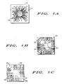
- FIGS 1A, 1B and 1C are top views of various layers of a ceramic semiconductor package.
- FIG. 1A shows a first layer of ceramic material 10 having a first surface 12.
- the ceramic material employed in the layers that comprise the semiconductor package may be one of a number of composite materials that are well known in the art.
- Disposed on first surface 12 of first layer ceramic material 10 are a plurality of metal interconnect lines 14.
- Metal interconnect lines 14 are processed on first layer of ceramic material 10 by screen printing metal on first surface 12. This method is well known in the art and this type of package commonly employs tungsten alloys for metal interconnect lines 14.
- First layer of ceramic material 10 further includes a die opening 16 through which a die may be wire bonded to pads disposed on first surface 12.
- FIG. 1B shows a second layer of ceramic material 18 having a first surface 20.
- Second layer of ceramic material 18 is of the same type of material as first layer of ceramic material 10.
- a plurality of metal interconnect lines 22 are formed on first surface 20 of second layer ceramic material 18 by the method discussed above. Further, metal interconnect lines 22 include a die bond pad 24 on which a die will ultimately be bonded. It should be understood that die opening 16 (see FIG. 1A) will be aligned with die bond pad 24 when ceramic layers are bonded together.
- FIG. 1C shows a third layer of ceramic material 26 having a first surface 28.
- third layer of ceramic material 26 is of the same type of material employed in second layer of ceramic material 18 and first layer of ceramic material 10.
- First surface 28 includes metal interconnects 30 that are formed by methods discussed above.
- Third layer of ceramic material 26 also includes vias 32 which are employed to electrically connect the metal disposed on the various ceramic layers when vias 32 are filled with metal. Vias will be discussed presently.
- Layer 34 includes a ceramic layer 36 having a first surface 38 and a second surface 40. Disposed on first surface 38 of ceramic layer 36 is a metal layer 42 that comprises interconnect lines. A via 44 is shown to extend through ceramic layer 36 from metal layer 42. In this embodiment, via 44 is filled with metal. Via 44 allows for the interconnect lines of metal layer 42 to extend to interconnect lines disposed on other layers of the ceramic semiconductor package thereby selectively connecting the various layers of metal interconnect lines. It should be understood that a typical multilayer ceramic semiconductor package will include numerous vias 44. It should further be understood by one skilled in the art that not all ceramic semiconductor packages employ vias 44. The various ceramic layers may be electrically connected to each other by the use of metal patterns along the outside of the package.
- first layer of ceramic material 10, second layer of ceramic 18 and third layer of ceramic material 26 are positioned in a predetermined relationship and bonded together by methods well known in the art to form a multilayer ceramic semiconductor package.
- metal interconnect lines 14 may be electrically connected to metal interconnect lines 22 which in turn may be connect to metal interconnects 30 by vias such as that shown in FIG. 2.
- other layers may be included in the multilayer ceramic semiconductor package.
- a ceramic semiconductor package comprised of a single layer of ceramic material having metal interconnect lines formed thereon may also be employed.
- metal pins are commonly used. The metal pins are are electrically connected to the internal metal and attached to the package by methods well known in the art such as brazing.
- FIG. 3 a highly enlarged top view of a corner of a layer of a ceramic semiconductor package is shown.
- the ceramic layers of a semiconductor package such as ceramic layer 36 shown here, are comprised of a composite material. Therefore, ceramic layer 36 is not of uniform density throughout.
- microcracks 46 occur and propagate in the ceramic. This commonly occurs in the corners of a ceramic semiconductor package. Microcrack 46 will tend to propagate in the ceramic until it runs into metal which acts as a barrier for microcrack 46. Microcrack 46 decreases yield in ceramic semiconductor packages as well as decreasing lifetime of the device in which the package is used.
- metal crack arrestor patterns 48 are shown. These figures illustrate various configurations of metal crack arrestor patterns 48. Since the propagation of microcrack 46 is inhibited by metal, it has been discovered that metal crack arrestor patterns 48 disposed in the corners of ceramic layer 36 will act as a barrier to microcracks 46. Essentially, metal crack arrestor patterns 48 will stop the progression of microcrack 46 before it reaches the actual metal circuitry disposed on ceramic layer 36. It should be understood that metal crack arrestor patterns 48 are not electrically or physically connected to the metal interconnect lines disposed on ceramic layer 36 in this embodiment, but it is possible that they may be.
- Metal crack arrestor patterns 48 are formed using the same steps and same type metal (commonly tungsten alloys) used to form the metal interconnect lines. Therefore, no extra processing steps are necessary to form metal crack arrestor patterns 48.
- metal crack arrestor patterns 48 are only shown on one surface of ceramic layer 36 in this embodiment, metal crack arrestor patterns 48 may be formed on both surfaces. Further, it should be understood that metal crack arrestor patterns 48 may be formed on one or more of the ceramic layers of a multi-layer ceramic semiconductor package. It will also be understood that the metal crack arrestor can have configurations other than those illustrated. As an example, it can be one wide piece instead of a line configuration.
- metal crack arrestor patterns 48 improve thermal conduction throughout the ceramic semiconductor package because the additional metal allows for improved heat transfer in the package thereby reducing the severity of thermal shock to the package. Also, because the corners of these packages are made stronger by metal crack arrestor patterns 48, the package is less prone to chipping and requires less mechanical protection for transportation.
Landscapes
- Engineering & Computer Science (AREA)
- Microelectronics & Electronic Packaging (AREA)
- Production Of Multi-Layered Print Wiring Board (AREA)
- Lead Frames For Integrated Circuits (AREA)
- Led Device Packages (AREA)
- Wire Bonding (AREA)
Applications Claiming Priority (2)
| Application Number | Priority Date | Filing Date | Title |
|---|---|---|---|
| US220292 | 1988-07-18 | ||
| US07/220,292 US4922326A (en) | 1988-07-18 | 1988-07-18 | Ceramic semiconductor package having crack arrestor patterns |
Publications (3)
| Publication Number | Publication Date |
|---|---|
| EP0351602A2 true EP0351602A2 (fr) | 1990-01-24 |
| EP0351602A3 EP0351602A3 (fr) | 1991-04-03 |
| EP0351602B1 EP0351602B1 (fr) | 1994-05-25 |
Family
ID=22822955
Family Applications (1)
| Application Number | Title | Priority Date | Filing Date |
|---|---|---|---|
| EP89111822A Expired - Lifetime EP0351602B1 (fr) | 1988-07-18 | 1989-06-29 | Empaquetage céramique pour semi-conducteur comprenant une configuration contre les craquements |
Country Status (6)
| Country | Link |
|---|---|
| US (1) | US4922326A (fr) |
| EP (1) | EP0351602B1 (fr) |
| JP (1) | JP2671512B2 (fr) |
| KR (1) | KR0127135B1 (fr) |
| DE (1) | DE68915485T2 (fr) |
| MY (1) | MY104091A (fr) |
Families Citing this family (6)
| Publication number | Priority date | Publication date | Assignee | Title |
|---|---|---|---|---|
| JP2776457B2 (ja) * | 1992-12-29 | 1998-07-16 | インターナショナル・ビジネス・マシーンズ・コーポレイション | 半導体デバイスのクラックストップ形成方法及び半導体デバイス |
| DE4319944C2 (de) * | 1993-06-03 | 1998-07-23 | Schulz Harder Juergen | Mehrfach-Substrat sowie Verfahren zu seiner Herstellung |
| US5420455A (en) * | 1994-03-31 | 1995-05-30 | International Business Machines Corp. | Array fuse damage protection devices and fabrication method |
| JP4656126B2 (ja) * | 2002-08-13 | 2011-03-23 | 富士電機システムズ株式会社 | 半導体装置 |
| US7960814B2 (en) | 2007-08-08 | 2011-06-14 | Freescale Semiconductor, Inc. | Stress relief of a semiconductor device |
| US9190318B2 (en) | 2013-10-22 | 2015-11-17 | Globalfoundries Inc. | Method of forming an integrated crackstop |
Family Cites Families (2)
| Publication number | Priority date | Publication date | Assignee | Title |
|---|---|---|---|---|
| JPS5651846A (en) * | 1979-10-04 | 1981-05-09 | Fujitsu Ltd | Ic package |
| US4417392A (en) * | 1980-05-15 | 1983-11-29 | Cts Corporation | Process of making multi-layer ceramic package |
-
1988
- 1988-07-18 US US07/220,292 patent/US4922326A/en not_active Expired - Lifetime
-
1989
- 1989-06-29 EP EP89111822A patent/EP0351602B1/fr not_active Expired - Lifetime
- 1989-06-29 DE DE68915485T patent/DE68915485T2/de not_active Expired - Lifetime
- 1989-07-06 MY MYPI89000922A patent/MY104091A/en unknown
- 1989-07-14 KR KR89010021A patent/KR0127135B1/ko not_active Expired - Lifetime
- 1989-07-18 JP JP1183808A patent/JP2671512B2/ja not_active Expired - Lifetime
Also Published As
| Publication number | Publication date |
|---|---|
| EP0351602B1 (fr) | 1994-05-25 |
| EP0351602A3 (fr) | 1991-04-03 |
| DE68915485D1 (de) | 1994-06-30 |
| MY104091A (en) | 1993-11-30 |
| KR0127135B1 (en) | 1997-12-29 |
| DE68915485T2 (de) | 1994-12-08 |
| US4922326A (en) | 1990-05-01 |
| JPH0273655A (ja) | 1990-03-13 |
| JP2671512B2 (ja) | 1997-10-29 |
Similar Documents
| Publication | Publication Date | Title |
|---|---|---|
| US5081067A (en) | Ceramic package type semiconductor device and method of assembling the same | |
| US4302625A (en) | Multi-layer ceramic substrate | |
| US5097318A (en) | Semiconductor package and computer using it | |
| US6362529B1 (en) | Stacked semiconductor device | |
| EP0714127A2 (fr) | Boîtier pour semi-conducteur | |
| US20110180919A1 (en) | Multi-tiered integrated circuit package | |
| US4992628A (en) | Ceramic-glass integrated circuit package with ground plane | |
| JPS61502294A (ja) | 高密度icモジュ−ルアセンブリ | |
| GB2028584A (en) | Mounting and connector unit | |
| US4922326A (en) | Ceramic semiconductor package having crack arrestor patterns | |
| US4976814A (en) | Method of making a ceramic semiconductor package having crack arrestor patterns | |
| US5463255A (en) | Semiconductor integrated circuit device having an electrode pad including an extended wire bonding portion | |
| US4336088A (en) | Method of fabricating an improved multi-layer ceramic substrate | |
| US6853055B1 (en) | Radiation shielding die carrier package | |
| US6228468B1 (en) | High density ceramic BGA package and method for making same | |
| US5134246A (en) | Ceramic-glass integrated circuit package with integral ground and power planes | |
| JPH09298252A (ja) | 半導体パッケージ及びこれを用いた半導体装置 | |
| JPH0680873B2 (ja) | 回路基板 | |
| US5790386A (en) | High I/O density MLC flat pack electronic component | |
| JPH09213829A (ja) | Bga型i/oフォーマットを使用した高性能デジタルicパッケージ及びバイメタル充填バイア技術による単層セラミックス基板 | |
| JP4686907B2 (ja) | セラミック基板の製造方法 | |
| US5151773A (en) | Electronic circuit apparatus comprising a structure for sealing an electronic circuit | |
| AU1184388A (en) | Method for connecting leadless chip packages and articles | |
| JPH10321759A (ja) | 電子部品用パッケージ本体及び電子部品用パッケージ | |
| JPH07130909A (ja) | 窒化アルミニウム多層基板 |
Legal Events
| Date | Code | Title | Description |
|---|---|---|---|
| PUAI | Public reference made under article 153(3) epc to a published international application that has entered the european phase |
Free format text: ORIGINAL CODE: 0009012 |
|
| AK | Designated contracting states |
Kind code of ref document: A2 Designated state(s): DE FR GB IT |
|
| PUAL | Search report despatched |
Free format text: ORIGINAL CODE: 0009013 |
|
| AK | Designated contracting states |
Kind code of ref document: A3 Designated state(s): DE FR GB IT |
|
| 17P | Request for examination filed |
Effective date: 19910930 |
|
| 17Q | First examination report despatched |
Effective date: 19930312 |
|
| GRAA | (expected) grant |
Free format text: ORIGINAL CODE: 0009210 |
|
| AK | Designated contracting states |
Kind code of ref document: B1 Designated state(s): DE FR GB IT |
|
| PG25 | Lapsed in a contracting state [announced via postgrant information from national office to epo] |
Ref country code: IT Free format text: LAPSE BECAUSE OF FAILURE TO SUBMIT A TRANSLATION OF THE DESCRIPTION OR TO PAY THE FEE WITHIN THE PRE;WARNING: LAPSES OF ITALIAN PATENTS WITH EFFECTIVE DATE BEFORE 2007 MAY HAVE OCCURRED AT ANY TIME BEFORE 2007. THE CORRECT EFFECTIVE DATE MAY BE DIFFERENT FROM THE ONE RECORDED.SCRIBED TIME-LIMIT Effective date: 19940525 |
|
| REF | Corresponds to: |
Ref document number: 68915485 Country of ref document: DE Date of ref document: 19940630 |
|
| ET | Fr: translation filed | ||
| PLBE | No opposition filed within time limit |
Free format text: ORIGINAL CODE: 0009261 |
|
| STAA | Information on the status of an ep patent application or granted ep patent |
Free format text: STATUS: NO OPPOSITION FILED WITHIN TIME LIMIT |
|
| 26N | No opposition filed | ||
| REG | Reference to a national code |
Ref country code: GB Ref legal event code: 746 Effective date: 19990930 |
|
| REG | Reference to a national code |
Ref country code: GB Ref legal event code: IF02 |
|
| REG | Reference to a national code |
Ref country code: FR Ref legal event code: D6 |
|
| REG | Reference to a national code |
Ref country code: GB Ref legal event code: 732E |
|
| REG | Reference to a national code |
Ref country code: FR Ref legal event code: TP |
|
| PGFP | Annual fee paid to national office [announced via postgrant information from national office to epo] |
Ref country code: DE Payment date: 20080630 Year of fee payment: 20 |
|
| PGFP | Annual fee paid to national office [announced via postgrant information from national office to epo] |
Ref country code: GB Payment date: 20080506 Year of fee payment: 20 |
|
| REG | Reference to a national code |
Ref country code: GB Ref legal event code: PE20 Expiry date: 20090628 |
|
| PG25 | Lapsed in a contracting state [announced via postgrant information from national office to epo] |
Ref country code: GB Free format text: LAPSE BECAUSE OF EXPIRATION OF PROTECTION Effective date: 20090628 |
|
| PGFP | Annual fee paid to national office [announced via postgrant information from national office to epo] |
Ref country code: FR Payment date: 20080424 Year of fee payment: 20 |