EP0352664A1 - Dispositif de mémoire à semi-conducteur présentant des lignes de données moins sensibles aux influences des lignes voisines - Google Patents
Dispositif de mémoire à semi-conducteur présentant des lignes de données moins sensibles aux influences des lignes voisines Download PDFInfo
- Publication number
- EP0352664A1 EP0352664A1 EP89113474A EP89113474A EP0352664A1 EP 0352664 A1 EP0352664 A1 EP 0352664A1 EP 89113474 A EP89113474 A EP 89113474A EP 89113474 A EP89113474 A EP 89113474A EP 0352664 A1 EP0352664 A1 EP 0352664A1
- Authority
- EP
- European Patent Office
- Prior art keywords
- bit lines
- insulating film
- memory device
- source
- level insulating
- Prior art date
- Legal status (The legal status is an assumption and is not a legal conclusion. Google has not performed a legal analysis and makes no representation as to the accuracy of the status listed.)
- Withdrawn
Links
Images





Classifications
-
- H—ELECTRICITY
- H10—SEMICONDUCTOR DEVICES; ELECTRIC SOLID-STATE DEVICES NOT OTHERWISE PROVIDED FOR
- H10W—GENERIC PACKAGES, INTERCONNECTIONS, CONNECTORS OR OTHER CONSTRUCTIONAL DETAILS OF DEVICES COVERED BY CLASS H10
- H10W20/00—Interconnections in chips, wafers or substrates
- H10W20/40—Interconnections external to wafers or substrates, e.g. back-end-of-line [BEOL] metallisations or vias connecting to gate electrodes
- H10W20/41—Interconnections external to wafers or substrates, e.g. back-end-of-line [BEOL] metallisations or vias connecting to gate electrodes characterised by their conductive parts
- H10W20/435—Cross-sectional shapes or dispositions of interconnections
-
- H—ELECTRICITY
- H10—SEMICONDUCTOR DEVICES; ELECTRIC SOLID-STATE DEVICES NOT OTHERWISE PROVIDED FOR
- H10B—ELECTRONIC MEMORY DEVICES
- H10B12/00—Dynamic random access memory [DRAM] devices
- H10B12/30—DRAM devices comprising one-transistor - one-capacitor [1T-1C] memory cells
- H10B12/31—DRAM devices comprising one-transistor - one-capacitor [1T-1C] memory cells having a storage electrode stacked over the transistor
-
- H—ELECTRICITY
- H10—SEMICONDUCTOR DEVICES; ELECTRIC SOLID-STATE DEVICES NOT OTHERWISE PROVIDED FOR
- H10B—ELECTRONIC MEMORY DEVICES
- H10B12/00—Dynamic random access memory [DRAM] devices
- H10B12/30—DRAM devices comprising one-transistor - one-capacitor [1T-1C] memory cells
- H10B12/37—DRAM devices comprising one-transistor - one-capacitor [1T-1C] memory cells the capacitor being at least partially in a trench in the substrate
- H10B12/377—DRAM devices comprising one-transistor - one-capacitor [1T-1C] memory cells the capacitor being at least partially in a trench in the substrate having a storage electrode extension located over the transistor
-
- H—ELECTRICITY
- H10—SEMICONDUCTOR DEVICES; ELECTRIC SOLID-STATE DEVICES NOT OTHERWISE PROVIDED FOR
- H10W—GENERIC PACKAGES, INTERCONNECTIONS, CONNECTORS OR OTHER CONSTRUCTIONAL DETAILS OF DEVICES COVERED BY CLASS H10
- H10W20/00—Interconnections in chips, wafers or substrates
- H10W20/40—Interconnections external to wafers or substrates, e.g. back-end-of-line [BEOL] metallisations or vias connecting to gate electrodes
- H10W20/41—Interconnections external to wafers or substrates, e.g. back-end-of-line [BEOL] metallisations or vias connecting to gate electrodes characterised by their conductive parts
- H10W20/423—Shielding layers
Definitions
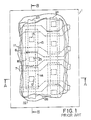
- the conductive film 18 is further covered with an interlevel insulating film 22, and bit lines 23 and 24 are patterned on the inter-level insulating film 22.
- the bit line 23 comes into contact with the common region 5 through a contact window 25 formed in the inter-level insulating film 22.
- the bit lines 23 and 24 are covered with an upper level insulating film 26 for providing a protection against vapor and contamination.
- bit line 23 is much liable to have influences of the adjacent bit lines if the gap therebetween is decreased. This is because of the fact that the bit lines are capacitively coupled to one another. In this circumstances, undesirable noises tends to ride on the data bit due to the capacitive coupling, and, accordingly, the sense amplifier cir cuit is liable to fail to correctly decide the logic level of the data bit.
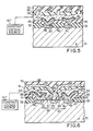
- the word lines 37, 39, 41 and 42 as well as exposed active area are covered with a lower insulating film 45, and contact windows 46 and 47 are formed in the lower insulating film 45 and expose the regions 33 and 36, respectively.
- On the lower insulating film 45 are provided accumulation electrodes 48, 49 and 50 or lower electrodes two of which have respective projections passing through the contact windows 46 and 47, thereby coming into contact with the regions 33 and 36, respectively.
- the accumulation electrodes 48, 49 and 50 of doped polycrystalline silicon are oxidized to form dielectric films 51, 52 and 53, re spectively, and the dielectric films 51 to 53 of silicon oxide are covered with a conductive film such as, for example, a doped polysilicon serving as a common electrode 54.
- the word line 37 goes up to the active high voltage level, and, accordingly, the data bit in the form of the electric charges is read out from the storage capacitor 55 to the bit line 68.
- the bit line 68 propagates the data bit to, for example, a sense amplifier circuit (not shown), and the sense amplifier circuit rapidly decides the logic level of the data bit.
- the data bit is less liable to be affected by the adjacent bit line 69, because any capacitive coupling hardly takes place between the bit lines 68 and 69 by virtue of the shield plate member 58. This results in that the random access memory device is free from any misreading of the data bit.
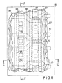
- FIGs. 8, 9 and 10 another random access memory device is shown and fabricated on a p-type semiconductor substrate 81.
- the random access memory device shown in Figs. 8 to 10 is similar in structure to that shown in Figs. 4 to 6 with the exception of storage capacitors 82 and 83, and, for this reason, description is made for the structure of each storage capacitors 82 and 83 only.
- the other component regions and films are designated by like reference numerals used for designations of the component regions and films in Figs. 4 to 6, and no detail description is incorporated for the sake of simplicity.
- the semiconductor substrate 81 is vertically removed to form a trench, and the wall is covered with a thin insulating film 84.
- the trench is filled with a conductive material serving as an accumulation electrode 85, and a narrow vertical cavity is formed in the accumulation electrode 85.
- the wall defining the narrow vertical cavity is thermally oxidized to form a dielectric film 86, and a conductive material such as a doped polysilicon is deposited on the dielectric film 86.
- the conductive material is patterned to form a common electrode 87, and the projections 57 to 59 or the shield plate members are projected from the common electrode 87.
Landscapes
- Semiconductor Memories (AREA)
Applications Claiming Priority (2)
| Application Number | Priority Date | Filing Date | Title |
|---|---|---|---|
| JP63186011A JPH0235771A (ja) | 1988-07-26 | 1988-07-26 | 半導体記憶装置 |
| JP186011/88 | 1988-07-26 |
Publications (1)
| Publication Number | Publication Date |
|---|---|
| EP0352664A1 true EP0352664A1 (fr) | 1990-01-31 |
Family
ID=16180817
Family Applications (1)
| Application Number | Title | Priority Date | Filing Date |
|---|---|---|---|
| EP89113474A Withdrawn EP0352664A1 (fr) | 1988-07-26 | 1989-07-21 | Dispositif de mémoire à semi-conducteur présentant des lignes de données moins sensibles aux influences des lignes voisines |
Country Status (3)
| Country | Link |
|---|---|
| US (1) | US4962476A (fr) |
| EP (1) | EP0352664A1 (fr) |
| JP (1) | JPH0235771A (fr) |
Cited By (2)
| Publication number | Priority date | Publication date | Assignee | Title |
|---|---|---|---|---|
| EP0475280A1 (fr) * | 1990-09-10 | 1992-03-18 | Sony Corporation | Dispositif à mémoire semi-conducteur |
| FR2690026A1 (fr) * | 1991-11-28 | 1993-10-15 | Samsung Electronics Co Ltd | Dispositif de mémoire destiné à supprimer le bruit produit entre des lignes de signaux. |
Families Citing this family (18)
| Publication number | Priority date | Publication date | Assignee | Title |
|---|---|---|---|---|
| JP3049100B2 (ja) * | 1991-03-04 | 2000-06-05 | 富士通株式会社 | 半導体装置及びその製造方法 |
| JP3357382B2 (ja) * | 1991-05-28 | 2002-12-16 | 株式会社日立製作所 | 多ポートメモリ |
| US5170243A (en) * | 1991-11-04 | 1992-12-08 | International Business Machines Corporation | Bit line configuration for semiconductor memory |
| US5135889A (en) * | 1991-12-09 | 1992-08-04 | Micron Technology, Inc. | Method for forming a shielding structure for decoupling signal traces in a semiconductor |
| JPH05218349A (ja) * | 1992-02-04 | 1993-08-27 | Sony Corp | 半導体記憶装置 |
| US5383151A (en) * | 1993-08-02 | 1995-01-17 | Sharp Kabushiki Kaisha | Dynamic random access memory |
| US6255852B1 (en) | 1999-02-09 | 2001-07-03 | Micron Technology, Inc. | Current mode signal interconnects and CMOS amplifier |
| US6373740B1 (en) * | 1999-07-30 | 2002-04-16 | Micron Technology, Inc. | Transmission lines for CMOS integrated circuits |
| US7554829B2 (en) | 1999-07-30 | 2009-06-30 | Micron Technology, Inc. | Transmission lines for CMOS integrated circuits |
| US7101770B2 (en) * | 2002-01-30 | 2006-09-05 | Micron Technology, Inc. | Capacitive techniques to reduce noise in high speed interconnections |
| US6900116B2 (en) | 2002-03-13 | 2005-05-31 | Micron Technology Inc. | High permeability thin films and patterned thin films to reduce noise in high speed interconnections |
| US6846738B2 (en) * | 2002-03-13 | 2005-01-25 | Micron Technology, Inc. | High permeability composite films to reduce noise in high speed interconnects |
| US7235457B2 (en) | 2002-03-13 | 2007-06-26 | Micron Technology, Inc. | High permeability layered films to reduce noise in high speed interconnects |
| US7160577B2 (en) | 2002-05-02 | 2007-01-09 | Micron Technology, Inc. | Methods for atomic-layer deposition of aluminum oxides in integrated circuits |
| US7192892B2 (en) | 2003-03-04 | 2007-03-20 | Micron Technology, Inc. | Atomic layer deposited dielectric layers |
| KR100522943B1 (ko) * | 2003-04-25 | 2005-10-25 | 학교법인고려중앙학원 | 소자 크기 변화에 무관하게 작고 안정한 바이어스 자기장을 갖는 자기 저항 구조 |
| US6970053B2 (en) * | 2003-05-22 | 2005-11-29 | Micron Technology, Inc. | Atomic layer deposition (ALD) high permeability layered magnetic films to reduce noise in high speed interconnection |
| US7927948B2 (en) | 2005-07-20 | 2011-04-19 | Micron Technology, Inc. | Devices with nanocrystals and methods of formation |
Citations (2)
| Publication number | Priority date | Publication date | Assignee | Title |
|---|---|---|---|---|
| EP0112670A1 (fr) * | 1982-12-20 | 1984-07-04 | Fujitsu Limited | Dispositif de mémoire à semi-conducteurs pourvu de cellules de mémoire à capacité empilées |
| EP0246458A2 (fr) * | 1986-05-19 | 1987-11-25 | International Business Machines Corporation | Module pour l'empaquetage de puces semi-conductrices à circuit intégré sur un substrat de base |
Family Cites Families (1)
| Publication number | Priority date | Publication date | Assignee | Title |
|---|---|---|---|---|
| JPH0797625B2 (ja) * | 1986-11-19 | 1995-10-18 | 三菱電機株式会社 | 半導体記憶装置 |
-
1988
- 1988-07-26 JP JP63186011A patent/JPH0235771A/ja active Pending
-
1989
- 1989-07-21 US US07/383,397 patent/US4962476A/en not_active Expired - Lifetime
- 1989-07-21 EP EP89113474A patent/EP0352664A1/fr not_active Withdrawn
Patent Citations (2)
| Publication number | Priority date | Publication date | Assignee | Title |
|---|---|---|---|---|
| EP0112670A1 (fr) * | 1982-12-20 | 1984-07-04 | Fujitsu Limited | Dispositif de mémoire à semi-conducteurs pourvu de cellules de mémoire à capacité empilées |
| EP0246458A2 (fr) * | 1986-05-19 | 1987-11-25 | International Business Machines Corporation | Module pour l'empaquetage de puces semi-conductrices à circuit intégré sur un substrat de base |
Non-Patent Citations (1)
| Title |
|---|
| IBM TECHNICAL DISCLOSURE BULLETIN, vol. 21 no. 12, May 1979, page 4827, New York, US; J.R. CAVALIERE et al.: "Reduction of capacitive coupling between adjacent dielectrically supported conductors" * |
Cited By (3)
| Publication number | Priority date | Publication date | Assignee | Title |
|---|---|---|---|---|
| EP0475280A1 (fr) * | 1990-09-10 | 1992-03-18 | Sony Corporation | Dispositif à mémoire semi-conducteur |
| US5424235A (en) * | 1990-09-10 | 1995-06-13 | Sony Corporation | Semiconductor memory device |
| FR2690026A1 (fr) * | 1991-11-28 | 1993-10-15 | Samsung Electronics Co Ltd | Dispositif de mémoire destiné à supprimer le bruit produit entre des lignes de signaux. |
Also Published As
| Publication number | Publication date |
|---|---|
| JPH0235771A (ja) | 1990-02-06 |
| US4962476A (en) | 1990-10-09 |
Similar Documents
| Publication | Publication Date | Title |
|---|---|---|
| EP0352664A1 (fr) | Dispositif de mémoire à semi-conducteur présentant des lignes de données moins sensibles aux influences des lignes voisines | |
| JP2929430B2 (ja) | キャパシタがないdramおよびその製造方法 | |
| KR900003908B1 (ko) | 2층 구조의 다이나믹 랜덤 액세스 메모리(dram) 셀 | |
| US5043780A (en) | DRAM cell having a texturized polysilicon lower capacitor plate for increased capacitance | |
| KR940005888B1 (ko) | 반도체기억장치 및 그 제조방법 | |
| US5047817A (en) | Stacked capacitor for semiconductor memory device | |
| KR20010015476A (ko) | 반도체 장치 | |
| JPS6050065B2 (ja) | メモリセル | |
| JP3158462B2 (ja) | 半導体記憶装置及びその製造方法 | |
| US5005072A (en) | Stacked cell design for 16-megabit DRAM array having a pair of interconnected poly layers which enfold a single field plate layer and connect to the cell's storage node junction | |
| KR930010823B1 (ko) | 반도체 기억장치 | |
| JPH029165A (ja) | 半導体メモリ | |
| JP2939536B2 (ja) | Dramセル、dram、及びその製造方法 | |
| US5219779A (en) | Memory cell for dynamic random access memory | |
| US5766995A (en) | Method for forming a DRAM cell with a ragged polysilicon crown-shaped capacitor | |
| US5030586A (en) | Method for manufacturing semiconductor memory device having improved resistance to α particle induced soft errors | |
| US4513304A (en) | Semiconductor memory device and process for producing the same | |
| US5057893A (en) | Static RAM cell with soft error immunity | |
| JP2001203277A (ja) | 半導体記憶装置およびその駆動方法 | |
| US4264965A (en) | Dummy cell structure for MIS dynamic memories | |
| JPH0576785B2 (fr) | ||
| US5170372A (en) | Memory device having bit lines over a field oxide | |
| JPH0982904A (ja) | ダイナミック型メモリ及びその製造方法 | |
| JPH05110019A (ja) | 半導体メモリ装置 | |
| US5905281A (en) | Draw cell with a fork-shaped capacitor |
Legal Events
| Date | Code | Title | Description |
|---|---|---|---|
| PUAI | Public reference made under article 153(3) epc to a published international application that has entered the european phase |
Free format text: ORIGINAL CODE: 0009012 |
|
| 17P | Request for examination filed |
Effective date: 19890721 |
|
| AK | Designated contracting states |
Kind code of ref document: A1 Designated state(s): DE FR GB |
|
| 17Q | First examination report despatched |
Effective date: 19931230 |
|
| STAA | Information on the status of an ep patent application or granted ep patent |
Free format text: STATUS: THE APPLICATION IS DEEMED TO BE WITHDRAWN |
|
| 18D | Application deemed to be withdrawn |
Effective date: 19950609 |