EP0352767A2 - Dispositif de prise d'images à l'état solide comportant une ligne de sortie partagée pour tension de conversion photo-électrique - Google Patents
Dispositif de prise d'images à l'état solide comportant une ligne de sortie partagée pour tension de conversion photo-électrique Download PDFInfo
- Publication number
- EP0352767A2 EP0352767A2 EP89113787A EP89113787A EP0352767A2 EP 0352767 A2 EP0352767 A2 EP 0352767A2 EP 89113787 A EP89113787 A EP 89113787A EP 89113787 A EP89113787 A EP 89113787A EP 0352767 A2 EP0352767 A2 EP 0352767A2
- Authority
- EP
- European Patent Office
- Prior art keywords
- charge
- output
- image pickup
- pulse
- pickup device
- Prior art date
- Legal status (The legal status is an assumption and is not a legal conclusion. Google has not performed a legal analysis and makes no representation as to the accuracy of the status listed.)
- Granted
Links
Images




Classifications
-
- H—ELECTRICITY
- H04—ELECTRIC COMMUNICATION TECHNIQUE
- H04N—PICTORIAL COMMUNICATION, e.g. TELEVISION
- H04N25/00—Circuitry of solid-state image sensors [SSIS]; Control thereof
- H04N25/70—SSIS architectures; Circuits associated therewith
- H04N25/71—Charge-coupled device [CCD] sensors; Charge-transfer registers specially adapted for CCD sensors
- H04N25/75—Circuitry for providing, modifying or processing image signals from the pixel array
-
- H—ELECTRICITY
- H04—ELECTRIC COMMUNICATION TECHNIQUE
- H04N—PICTORIAL COMMUNICATION, e.g. TELEVISION
- H04N25/00—Circuitry of solid-state image sensors [SSIS]; Control thereof
- H04N25/70—SSIS architectures; Circuits associated therewith
- H04N25/76—Addressed sensors, e.g. MOS or CMOS sensors
- H04N25/767—Horizontal readout lines, multiplexers or registers
-
- H—ELECTRICITY
- H10—SEMICONDUCTOR DEVICES; ELECTRIC SOLID-STATE DEVICES NOT OTHERWISE PROVIDED FOR
- H10F—INORGANIC SEMICONDUCTOR DEVICES SENSITIVE TO INFRARED RADIATION, LIGHT, ELECTROMAGNETIC RADIATION OF SHORTER WAVELENGTH OR CORPUSCULAR RADIATION
- H10F39/00—Integrated devices, or assemblies of multiple devices, comprising at least one element covered by group H10F30/00, e.g. radiation detectors comprising photodiode arrays
- H10F39/10—Integrated devices
- H10F39/12—Image sensors
- H10F39/18—Complementary metal-oxide-semiconductor [CMOS] image sensors; Photodiode array image sensors
Definitions
- This invention relates to a solid-state image pickup device.
- CCD linear image sensors For the linear image sensor, CCD linear image sensors, image sensors of the contact type using amorphous silicon and the like, have been conventionally used.
- FIG. 1 there is shown a fundamental configuration of a solid-state image pickup device according to this invention.
- a shift register 2 photosensitive pixels PE1, ..., PE n , charge/voltage conversion elements A1, ..., A n , a current source 4, and an element-shared output line 5 are integrated.
- the semiconductor substrate 1 is provided with terminals 8a, 8b, 8c, 8d, 8e, 8f and 8g.
- drive pulse ⁇ 1 and ⁇ 2 are steadily applied from the external through terminals 8a and 8b, respectively.
- a start pulse ⁇ * is applied at time of t1.
- a d.c. voltage of 5V is applied to the source side of the MOS transistor M01 of the starter circuit SR0 through the terminal 8d shown in FIG. 1.
- start pulse ⁇ * is applied to the gate of the MOS transistor M01 at time t1
- a potential ⁇ a on the point a on the drain side of the transistor M01 is raised from low level to reach a value less than 5V.
- the start pulse ⁇ * shifts from high level to low level at time t2
- the potential ⁇ a on the point a remains at a value less than 5V by the influence of the capacitor C0.
- This potential ⁇ a is applied to the gate of the transistor M02. However, since the drive pulse ⁇ 2 is at low level, the potential ⁇ b on the point b is also at low level. Such a state is continued until the drive pulse ⁇ 2 shifts from low to high level at time t4.
- the potential ⁇ b on the point b is raised. Accordingly, the potential ⁇ a on the point a is raised by the step-up action to reach a value less than 5V as shown in FIG. 3. Such a state is continued until time t5. Since the drive pulse ⁇ 2 shifts from high to low level at time t5, the potential ⁇ b on the point b also shifts from high to low level. Accordingly, the potential ⁇ a on the point a is also lowered from a value larger than 5V to a value lower than 5V.
- a d.c. voltage of 5V is applied through terminal 8d shown in FIG. 1 to the source side of the transistor M11 of the control pulse generation circuit SR1. Since the potential ⁇ b is applied to the gate of the transistor M11, a potential ⁇ c on the point c on the drain side of the transistor M11 is raised from low level to a value lower than 5V in the same manner as in the case of the potential ⁇ a on the point a of the start circuit SR0. Such a state is continued until the time t6 when the drive pulse applied to the source side of the transistor M12 shifts from low to high level.
- the potential ⁇ d on the point d also shifts from high to low level. Accordingly, the potential ⁇ c on the point c is also lowered from a value larger than 5V to a value smaller than 5V.
- control pulses ⁇ S2 and ⁇ B2 are taken out from the control pulse generation circuit SR2 in the same manner as in the case of the control pulse generation circuit SR1. These pulses thus taken out are output to the charge/voltage conversion element A2.
- the output V out of the charge/voltage conversion element A i specifically output to the common line 5 is output to the external through the terminal 8g.
- the photodiode PE i is constituted, e.g., as shown in FIG. 5, by forming a P-well on an N type semiconductor substrate to form an n type semiconductor substrate to form an n region and a P+ region on the side of the surface of the P-well.
- LOCOS represents a selective oxidation structure of the silicon substrate by a silicon nitride film and is an abbreviation of localized oxidation of silicon.
- n+ regions are separately formed on the side of the surface of the P-well, and one n+ region thereof is in contact with the n region.
- the n+ region and an electrode formed between two n+ regions constitute the above-mentioned reset transistor 12.
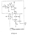
- a d.c. voltage of 5V is applied to the source and the gate of the transistor 14 through the terminal 8d shown in FIG. 1 (see FIG. 4).
- a potential ⁇ ⁇ on the point ⁇ shown in FIG. 4 is slightly raised from low level to reach a predetermined level (see FIG. 6). Since the control pulse ⁇ Si shifts to high level at time T2, the potential ⁇ ⁇ shifts to a standby level. Since the reset pulse ⁇ R shifts from low to high level at time T3, the potential ⁇ ⁇ on the point ⁇ is raised by the step-up action to reach a predetermined level (hereinafter referred to as a reset level). Since the reset pulse ⁇ R shifts from high to low level at time T4, the potential ⁇ ⁇ shifts to the standby level for a second time. This standby level is continued until T5.
- the transistor 19 When the control pulse ⁇ Si is at the maximum level (from T2 to T5), the transistor 19 becomes active as a source-follower circuit. For a time period during which the pulse ⁇ RSi is at the standby level and the control pulse ⁇ Si is at the maximum level (from T2 to T3), a potential ⁇ ⁇ corresponding to a quantity of signal charges stored in the capacitor 11 after the last reset operation until T2 is detected at the source follower circuit. For a time period during which the pulse ⁇ RSi is at reset level and the control pulse ⁇ Si is at the maximum level (from t3 to t4), the potential ⁇ ⁇ across the capacitor 11 is reset.
- the solid-state image pickup device comprises the charge/voltage conversion element having the circuitry shown in FIG. 4 and driven by the control pulse of 5V
- the device of the present invention is not restricted in the first embodiment and is applicable to the second embodiment having the configuration and function each shown in FIGS. 7 to 9.
- FIG. 7 shows the entire configuration of a solid-state image pickup device according to the second embodiment.
- elements having the same numerals of FIGS. 1, 4 and 5 are the same or equivalent elements thereof, duplicate explanation will be omitted.
- the second embodiment is different from the first embodiment having the conversion element shown in FIG. 4 at two points hereinafter.
- the first is when the image pickup device is formed in a chip, the capacitors for raising the voltage occupy large areas within a chip.
- the conversion element according to the second embodiment does not have capacitors for raising the voltage, and so the chip of a device can be integrated higher.
- the second embodiment it is possible for the second embodiment to form a solid-state image sensor into a multichip circuit in which a plurality of chips are interconnected with each other after each chip of the image pickup device is completed on the semiconductor substrate 1. Therefore, a chip-shared output line 9 is provided for interconnecting the chips in each chip.
- a conversion element A i of the second embodiment is driven by a 12V control voltage different to the 5V of the first embodiment.
- the chip-shared line 9 for interconnecting chips and achieving a multichip has in both ends an input terminal 8g1 having a current source 6, and an output terminal 8g2 to which the element-shared output line 5 is connected through a buffer 7.
- the buffer 7 is provided for output voltage of the element-shared line 5 to the chip-shared line 9 having the low impedance.
- the current source 6 and buffer 7 form a source follower circuit.
- the element A i functions for potential detection and output of the pixel PE i . Namely, the electric charges of the pixel PE i following in a capacitor 36 (CP i ) are charged therein and then, two-stage source followers read out the change of potential between both ends of the capacitor 36 (CP i ). After reading out the potential change, a reset pulse ⁇ R impressed from the outside resets and equalizes the potential of both ends of the capacitor 36 (CP i ) to an external power source ⁇ .
- the two-stage source followers comprise a first stage source follower 40 which is controlled in operation by a set pulse ⁇ Si , and a second stage source follower which is controlled by the first stage source follower 40.
- the second stage source follower concretely comprises the current source 4 and driver 31.
- a numeral 32 denotes a gate for selecting the conversion element and then, while the gate 32 opens by the set pulse ⁇ Si and output of the driver 31, the conversion element having the open gate 32 outputs a converted voltage to the element-shared output line 5.
- a shift register comprises a first shift register 2A for generating a set pulse ⁇ Si , and a second shift register 2B for generating a clear pulse ⁇ Ci which is made in each chip on the basis of the reset pulse ⁇ R supplied from the outside.
- the external power source ⁇ is supplied the terminal 8d of the chip in the same manner as the first embodiment.
- the first stage source follower 40 comprises MOS (metal oxide semiconductor) transistors 25 and 26 forming a voltage divider circuit 27 which generates a load-bias voltage in response to the set pulse ⁇ Si , a driver 29 to which the voltage of the capacitor 36 is impressed, and a current source 30 to which the voltage divided by the divider 27 is impressed.
- MOS metal oxide semiconductor
- the output of the first stage source follower 40 is determined by both waveforms of the nodes ⁇ and ⁇ . Accordingly, the pulse waveform of the node ⁇ between the driver 29 and current source 30, as shown in FIG. 9, falls gradually until time T2 and abruptly at time T2. At time T3, the voltage of the node ⁇ raises with an amount of the potential difference Dp corresponding to the quantity of light sensed by pixel PE i , and falls at time T4. After the waveform of the node ⁇ falls gradually between times T4 and T5, raises again at the time T5, and falls gradually after the time T5. Thus, the waveform of node ⁇ is controlled in the offset and impedance on the basis of waveforms of the nodes ⁇ and ⁇ .
- the element-shared line 5 is sequentially supplied with the outputs of each element A i , that is, elements A1 to A n . Accordingly, the waveform of node ⁇ between times T2 to T5 is repeatedly output to the node ⁇ of the shared line 5 every time the driving pulse of the shift register 2 is raised, so that output pulses can be read out in response to the quantity of light sensed by the pixel PE i .
- times T1 and T6 which are the adjacent raising times of the driving pulse ⁇ 2, do not relate directly to the output pulses of the node ⁇ because the element A i of the second embodiment does not operate for raising the voltage.
Landscapes
- Engineering & Computer Science (AREA)
- Multimedia (AREA)
- Signal Processing (AREA)
- Transforming Light Signals Into Electric Signals (AREA)
- Solid State Image Pick-Up Elements (AREA)
- Facsimile Heads (AREA)
Applications Claiming Priority (4)
| Application Number | Priority Date | Filing Date | Title |
|---|---|---|---|
| JP186366/88 | 1988-07-26 | ||
| JP18636688 | 1988-07-26 | ||
| JP63279105A JPH0795829B2 (ja) | 1988-07-26 | 1988-11-04 | 固体撮像装置 |
| JP279105/88 | 1988-11-04 |
Publications (3)
| Publication Number | Publication Date |
|---|---|
| EP0352767A2 true EP0352767A2 (fr) | 1990-01-31 |
| EP0352767A3 EP0352767A3 (fr) | 1992-05-20 |
| EP0352767B1 EP0352767B1 (fr) | 1997-10-01 |
Family
ID=26503717
Family Applications (1)
| Application Number | Title | Priority Date | Filing Date |
|---|---|---|---|
| EP89113787A Expired - Lifetime EP0352767B1 (fr) | 1988-07-26 | 1989-07-26 | Dispositif de prise d'images à l'état solide comportant une ligne de sortie partagée pour tension de conversion photo-électrique |
Country Status (4)
| Country | Link |
|---|---|
| US (1) | US5012344A (fr) |
| EP (1) | EP0352767B1 (fr) |
| JP (1) | JPH0795829B2 (fr) |
| DE (1) | DE68928357T2 (fr) |
Cited By (2)
| Publication number | Priority date | Publication date | Assignee | Title |
|---|---|---|---|---|
| WO1995033332A3 (fr) * | 1994-06-01 | 1996-01-18 | Simage Oy | Dispositifs, systemes et procedes de generation d'images |
| US6035013A (en) * | 1994-06-01 | 2000-03-07 | Simage O.Y. | Radiographic imaging devices, systems and methods |
Families Citing this family (13)
| Publication number | Priority date | Publication date | Assignee | Title |
|---|---|---|---|---|
| JP3097121B2 (ja) * | 1990-09-27 | 2000-10-10 | ソニー株式会社 | 電荷/電圧変換効率の測定方法 |
| JPH04199968A (ja) * | 1990-11-29 | 1992-07-21 | Toshiba Corp | 固体撮像装置 |
| CA2060556A1 (fr) * | 1992-02-03 | 1993-08-04 | Savvas G. Chamberlain | Structure de sortie haute frequence bimode a differenciation de pixels montee sur une puce de capteur d'image a transfert de charge |
| US5450549A (en) * | 1992-04-09 | 1995-09-12 | International Business Machines Corporation | Multi-channel image array buffer and switching network |
| US5461425A (en) * | 1994-02-15 | 1995-10-24 | Stanford University | CMOS image sensor with pixel level A/D conversion |
| JPH08149376A (ja) * | 1994-11-18 | 1996-06-07 | Olympus Optical Co Ltd | 固体撮像装置 |
| JPH1098176A (ja) | 1996-09-19 | 1998-04-14 | Toshiba Corp | 固体撮像装置 |
| US6657665B1 (en) * | 1998-12-31 | 2003-12-02 | Eastman Kodak Company | Active Pixel Sensor with wired floating diffusions and shared amplifier |
| US6975355B1 (en) | 2000-02-22 | 2005-12-13 | Pixim, Inc. | Multiple sampling via a time-indexed method to achieve wide dynamic ranges |
| US7095439B2 (en) | 2002-04-04 | 2006-08-22 | Motorola, Inc. | Image sensor circuit and method |
| JP2004228873A (ja) * | 2003-01-22 | 2004-08-12 | Seiko Epson Corp | 画像処理装置、画像処理方法及び固体撮像装置 |
| JP3951994B2 (ja) * | 2003-09-16 | 2007-08-01 | ソニー株式会社 | 固体撮像装置およびカメラシステム |
| JP2004349715A (ja) * | 2004-06-21 | 2004-12-09 | Sony Corp | イメージセンサ |
Family Cites Families (13)
| Publication number | Priority date | Publication date | Assignee | Title |
|---|---|---|---|---|
| JPS5521472B2 (fr) * | 1971-08-11 | 1980-06-10 | ||
| JPS5528456B2 (fr) * | 1972-11-08 | 1980-07-28 | ||
| JPS50134393A (fr) * | 1974-04-10 | 1975-10-24 | ||
| US4023048A (en) * | 1975-12-15 | 1977-05-10 | International Business Machines Corporation | Self-scanning photo-sensitive circuits |
| JPS5343416A (en) * | 1976-10-01 | 1978-04-19 | Hitachi Ltd | Image sensor |
| JPS59140766A (ja) * | 1983-02-01 | 1984-08-13 | Fuji Xerox Co Ltd | 原稿読取装置 |
| US4617471A (en) * | 1983-12-27 | 1986-10-14 | Kabushiki Kaisha Toshiba | Image sensing device |
| US4763007A (en) * | 1984-12-25 | 1988-08-09 | Ricoh Company, Ltd. | Image sensor driving circuit |
| US4914519A (en) * | 1986-09-19 | 1990-04-03 | Canon Kabushiki Kaisha | Apparatus for eliminating noise in a solid-state image pickup device |
| US4737854A (en) * | 1986-07-18 | 1988-04-12 | Xerox Corporation | Image sensor array with two stage transfer |
| JPS6364469A (ja) * | 1986-09-05 | 1988-03-22 | Toshiba Corp | イメ−ジセンサ |
| US4858022A (en) * | 1986-09-05 | 1989-08-15 | Kabushiki Kaisha Toshiba | Contact-type linear image sensor |
| JPH084129B2 (ja) * | 1986-11-19 | 1996-01-17 | キヤノン株式会社 | 光電変換装置 |
-
1988
- 1988-11-04 JP JP63279105A patent/JPH0795829B2/ja not_active Expired - Fee Related
-
1989
- 1989-07-26 DE DE68928357T patent/DE68928357T2/de not_active Expired - Fee Related
- 1989-07-26 US US07/385,159 patent/US5012344A/en not_active Expired - Lifetime
- 1989-07-26 EP EP89113787A patent/EP0352767B1/fr not_active Expired - Lifetime
Cited By (3)
| Publication number | Priority date | Publication date | Assignee | Title |
|---|---|---|---|---|
| WO1995033332A3 (fr) * | 1994-06-01 | 1996-01-18 | Simage Oy | Dispositifs, systemes et procedes de generation d'images |
| US5812191A (en) * | 1994-06-01 | 1998-09-22 | Simage Oy | Semiconductor high-energy radiation imaging device |
| US6035013A (en) * | 1994-06-01 | 2000-03-07 | Simage O.Y. | Radiographic imaging devices, systems and methods |
Also Published As
| Publication number | Publication date |
|---|---|
| EP0352767B1 (fr) | 1997-10-01 |
| JPH02131681A (ja) | 1990-05-21 |
| DE68928357D1 (de) | 1997-11-06 |
| US5012344A (en) | 1991-04-30 |
| EP0352767A3 (fr) | 1992-05-20 |
| JPH0795829B2 (ja) | 1995-10-11 |
| DE68928357T2 (de) | 1998-02-19 |
Similar Documents
| Publication | Publication Date | Title |
|---|---|---|
| EP0260956B1 (fr) | Appareil de conversion photo-électrique | |
| EP0352767A2 (fr) | Dispositif de prise d'images à l'état solide comportant une ligne de sortie partagée pour tension de conversion photo-électrique | |
| EP0493455B1 (fr) | Detecteur de circuit integre | |
| US6731335B1 (en) | CMOS image sensor having common outputting transistors and method for driving the same | |
| US5296696A (en) | Solid state image pickup apparatus and driving method | |
| US6525304B1 (en) | Circuitry for converting analog signals from pixel sensor to a digital and for storing the digital signal | |
| US7623170B2 (en) | Amplification type image pickup apparatus and method of controlling the amplification type image pickup apparatus | |
| US7697051B2 (en) | Image sensor with pixels having multiple capacitive storage elements | |
| US5493423A (en) | Resettable pixel amplifier for an image sensor array | |
| US6903771B2 (en) | Image pickup apparatus | |
| US6421085B1 (en) | High speed CMOS imager column CDS circuit | |
| KR20020046957A (ko) | 아날로그 상호 연관된 이중 샘플링 기능을 수행하는씨모스 이미지 센서용 비교 장치 | |
| US6791612B1 (en) | CMOS image sensor having a pixel array in a wider dynamic range | |
| US6346696B1 (en) | Image sensor and method for driving the same | |
| JP2575964B2 (ja) | 固体撮像装置 | |
| US4831451A (en) | Horizontal scanner for image sensor arrays | |
| JPH09247536A (ja) | Mos型固体撮像装置及びその駆動方法 | |
| US4752829A (en) | Multipacket charge transfer image sensor and method | |
| US4825292A (en) | Picture pick-up device including a solid-state sensor and operating with a signal interference reduction | |
| JP3008655B2 (ja) | 固体撮像装置 | |
| JP2000106652A (ja) | 固体撮像装置 | |
| JP3223823B2 (ja) | 固体撮像装置の出力回路およびその駆動方法 | |
| JP3449823B2 (ja) | 固体撮像装置の駆動方法 | |
| US5731833A (en) | Solid-state image pick-up device with reference level clamping and image pick-up apparatus using the same | |
| JPH08116491A (ja) | 光電変換装置 |
Legal Events
| Date | Code | Title | Description |
|---|---|---|---|
| PUAI | Public reference made under article 153(3) epc to a published international application that has entered the european phase |
Free format text: ORIGINAL CODE: 0009012 |
|
| 17P | Request for examination filed |
Effective date: 19890726 |
|
| AK | Designated contracting states |
Kind code of ref document: A2 Designated state(s): DE FR GB |
|
| PUAL | Search report despatched |
Free format text: ORIGINAL CODE: 0009013 |
|
| AK | Designated contracting states |
Kind code of ref document: A3 Designated state(s): DE FR GB |
|
| 17Q | First examination report despatched |
Effective date: 19930730 |
|
| GRAG | Despatch of communication of intention to grant |
Free format text: ORIGINAL CODE: EPIDOS AGRA |
|
| GRAH | Despatch of communication of intention to grant a patent |
Free format text: ORIGINAL CODE: EPIDOS IGRA |
|
| GRAH | Despatch of communication of intention to grant a patent |
Free format text: ORIGINAL CODE: EPIDOS IGRA |
|
| GRAA | (expected) grant |
Free format text: ORIGINAL CODE: 0009210 |
|
| AK | Designated contracting states |
Kind code of ref document: B1 Designated state(s): DE FR GB |
|
| REF | Corresponds to: |
Ref document number: 68928357 Country of ref document: DE Date of ref document: 19971106 |
|
| ET | Fr: translation filed | ||
| PLBE | No opposition filed within time limit |
Free format text: ORIGINAL CODE: 0009261 |
|
| STAA | Information on the status of an ep patent application or granted ep patent |
Free format text: STATUS: NO OPPOSITION FILED WITHIN TIME LIMIT |
|
| 26N | No opposition filed | ||
| REG | Reference to a national code |
Ref country code: GB Ref legal event code: 746 Effective date: 19981015 |
|
| REG | Reference to a national code |
Ref country code: FR Ref legal event code: D6 |
|
| REG | Reference to a national code |
Ref country code: GB Ref legal event code: IF02 |
|
| PGFP | Annual fee paid to national office [announced via postgrant information from national office to epo] |
Ref country code: FR Payment date: 20020709 Year of fee payment: 14 |
|
| PGFP | Annual fee paid to national office [announced via postgrant information from national office to epo] |
Ref country code: GB Payment date: 20020724 Year of fee payment: 14 |
|
| PGFP | Annual fee paid to national office [announced via postgrant information from national office to epo] |
Ref country code: DE Payment date: 20020731 Year of fee payment: 14 |
|
| PG25 | Lapsed in a contracting state [announced via postgrant information from national office to epo] |
Ref country code: GB Free format text: LAPSE BECAUSE OF NON-PAYMENT OF DUE FEES Effective date: 20030726 |
|
| PG25 | Lapsed in a contracting state [announced via postgrant information from national office to epo] |
Ref country code: DE Free format text: LAPSE BECAUSE OF NON-PAYMENT OF DUE FEES Effective date: 20040203 |
|
| GBPC | Gb: european patent ceased through non-payment of renewal fee |
Effective date: 20030726 |
|
| PG25 | Lapsed in a contracting state [announced via postgrant information from national office to epo] |
Ref country code: FR Free format text: LAPSE BECAUSE OF NON-PAYMENT OF DUE FEES Effective date: 20040331 |
|
| REG | Reference to a national code |
Ref country code: FR Ref legal event code: ST |