EP0352767B1 - Festkörper-Bildaufnehmer mit gemeinsamer Ausgangsleitung für Spannungen aus photoelektrischer Umwandlung - Google Patents
Festkörper-Bildaufnehmer mit gemeinsamer Ausgangsleitung für Spannungen aus photoelektrischer Umwandlung Download PDFInfo
- Publication number
- EP0352767B1 EP0352767B1 EP89113787A EP89113787A EP0352767B1 EP 0352767 B1 EP0352767 B1 EP 0352767B1 EP 89113787 A EP89113787 A EP 89113787A EP 89113787 A EP89113787 A EP 89113787A EP 0352767 B1 EP0352767 B1 EP 0352767B1
- Authority
- EP
- European Patent Office
- Prior art keywords
- output line
- charge
- image pickup
- solid
- voltage
- Prior art date
- Legal status (The legal status is an assumption and is not a legal conclusion. Google has not performed a legal analysis and makes no representation as to the accuracy of the status listed.)
- Expired - Lifetime
Links
- 238000006243 chemical reaction Methods 0.000 title claims description 37
- 239000003990 capacitor Substances 0.000 claims description 28
- 239000004065 semiconductor Substances 0.000 claims description 9
- 239000000758 substrate Substances 0.000 claims description 9
- 230000004044 response Effects 0.000 claims description 6
- 230000008859 change Effects 0.000 claims description 3
- 229910044991 metal oxide Inorganic materials 0.000 claims description 2
- 150000004706 metal oxides Chemical class 0.000 claims description 2
- 238000010586 diagram Methods 0.000 description 7
- 230000010354 integration Effects 0.000 description 7
- 238000004519 manufacturing process Methods 0.000 description 5
- 230000009471 action Effects 0.000 description 4
- 239000007858 starting material Substances 0.000 description 4
- XUIMIQQOPSSXEZ-UHFFFAOYSA-N Silicon Chemical compound [Si] XUIMIQQOPSSXEZ-UHFFFAOYSA-N 0.000 description 2
- 229910021417 amorphous silicon Inorganic materials 0.000 description 2
- 230000015572 biosynthetic process Effects 0.000 description 2
- 230000003647 oxidation Effects 0.000 description 2
- 238000007254 oxidation reaction Methods 0.000 description 2
- 238000005070 sampling Methods 0.000 description 2
- 229910052710 silicon Inorganic materials 0.000 description 2
- 239000010703 silicon Substances 0.000 description 2
- 230000001360 synchronised effect Effects 0.000 description 2
- 229910052581 Si3N4 Inorganic materials 0.000 description 1
- 238000001514 detection method Methods 0.000 description 1
- 230000000694 effects Effects 0.000 description 1
- 229910021420 polycrystalline silicon Inorganic materials 0.000 description 1
- 229920005591 polysilicon Polymers 0.000 description 1
- HQVNEWCFYHHQES-UHFFFAOYSA-N silicon nitride Chemical compound N12[Si]34N5[Si]62N3[Si]51N64 HQVNEWCFYHHQES-UHFFFAOYSA-N 0.000 description 1
Images


Classifications
-
- H—ELECTRICITY
- H04—ELECTRIC COMMUNICATION TECHNIQUE
- H04N—PICTORIAL COMMUNICATION, e.g. TELEVISION
- H04N25/00—Circuitry of solid-state image sensors [SSIS]; Control thereof
- H04N25/70—SSIS architectures; Circuits associated therewith
- H04N25/76—Addressed sensors, e.g. MOS or CMOS sensors
- H04N25/767—Horizontal readout lines, multiplexers or registers
-
- H—ELECTRICITY
- H04—ELECTRIC COMMUNICATION TECHNIQUE
- H04N—PICTORIAL COMMUNICATION, e.g. TELEVISION
- H04N25/00—Circuitry of solid-state image sensors [SSIS]; Control thereof
- H04N25/70—SSIS architectures; Circuits associated therewith
- H04N25/71—Charge-coupled device [CCD] sensors; Charge-transfer registers specially adapted for CCD sensors
- H04N25/75—Circuitry for providing, modifying or processing image signals from the pixel array
-
- H—ELECTRICITY
- H10—SEMICONDUCTOR DEVICES; ELECTRIC SOLID-STATE DEVICES NOT OTHERWISE PROVIDED FOR
- H10F—INORGANIC SEMICONDUCTOR DEVICES SENSITIVE TO INFRARED RADIATION, LIGHT, ELECTROMAGNETIC RADIATION OF SHORTER WAVELENGTH OR CORPUSCULAR RADIATION
- H10F39/00—Integrated devices, or assemblies of multiple devices, comprising at least one element covered by group H10F30/00, e.g. radiation detectors comprising photodiode arrays
- H10F39/10—Integrated devices
- H10F39/12—Image sensors
- H10F39/18—Complementary metal-oxide-semiconductor [CMOS] image sensors; Photodiode array image sensors
Definitions
- This invention relates to a solid-state image pickup device.
- CCD linear image sensors For the linear image sensor, CCD linear image sensors, image sensors of the contact type using amorphous silicon and the like, have been conventionally used.
- EP-A-0 260 954 shows a device comprising shift registers for generating control signals, charge voltage conversion elements and an element-shared output line, but two capacitors are required, together with switching circuits for each pixel to separate reference signals and sensor signals.
- EP-A-0 254 497 shows a device including source-follower type charge/voltage conversion circuits.
- This invention has been made in view of the above-mentioned problems, and its object is to provide a solid-state image pickup device which has a simple manufacturing process, and which is capable of providing a sufficient SN ratio.
- this device adopts such a scheme to detect quantities of integration of signal charges and zero reference levels of the quantity of integration by the charge/voltage conversion elements to convert the values detected to corresponding voltage values, to therefore sequentially output them to the outside through the shared output line. This permits execution of processing, e.g., correlative double sampling, etc., resulting in a sufficient SN ratio.
- the manufacturing process is simple and a sufficient SN ratio can be obtained.
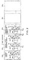
- FIG. 1 there is shown a fundamental configuration of a solid-state image pickup device.
- a shift register 2 photosensitive pixels PE 1 , ..., PE n , charge/voltage conversion elements A 1 , ..., A n , a current source 4, and an element-shared output line 5 are integrated.
- the semiconductor substrate 1 is provided with terminals 8a, 8b, 8c, 8d, 8e, 8f and 8g.
- drive pulses ⁇ 1 and ⁇ 2 are steadily applied from the external through terminals 8a and 8b, respectively.
- a start pulse ⁇ * is applied to the shift register 2 through terminal 8c, and a d.c. voltage (e.g., 5V or 12V) is applied to the shift register 2 and to charge/voltage conversion elements A 1 , ..., A n through terminal 8d.
- a reset pulse ⁇ R input through terminal 8e is applied to charge/voltage conversion elements A 1 , ..., A n .
- the terminal designated by reference numeral 8f serves as a ground terminal.
- the shift register 2 is composed of a starter circuit SR 0 and a number n of control pulse generation circuits SR 1 , ..., SR n .
- the starter circuit SR 0 is composed of four MOS transistors (hereinafter simply referred to as transistors, respectively) M 01 , ..., M 04 , and one capacitor C 0
- start pulse ⁇ ⁇ is applied at time of t 1 .
- a d.c. voltage of 5V is applied to the source side of the MOS transistor M 01 of the starter circuit SR 0 through the terminal 8d shown in FIG. 1.
- start pulse ⁇ ⁇ is applied to the gate of the MOS transistor M 01 at time t 1 , a potential ⁇ a on the point a on the drain side of the transistor M 01 is raised from low level to reach a value less than 5V.
- the potential ⁇ b on the point b is raised. Accordingly, the potential ⁇ a a on the point is raised by the step-up action to reach a value larger than 5V as shown in FIG. 3. Such a state is continued until time t 5 . Since the drive pulse ⁇ 2 shifts from high to low level at time t 5 , the potential ⁇ b on the point b also shifts from high to low level. Accordingly, the potential ⁇ a on the point a is also lowered from a value larger than 5V to a value lower than 5V.
- a d.c. voltage of 5V is applied through terminal 8d shown in FIG. 1 to the source side of the transistor M 11 of the control pulse generation circuit SR 1 . Since the potential ⁇ b is applied to the gate of the transistor M 11 , a potential ⁇ c on the point c on the drain side of the transistor M 11 is raised from low level to a value lower than 5V in the same manner as in the case of the potential ⁇ a on the point a of the start circuit SR 0 . Such a state is continued until the time t 6 when the drive pulse applied to the source side of the transistor M 12 shifts from low to high level.
- the potential ⁇ d on the point d also shifts from high to low level. Accordingly, the potential ⁇ c on the point c is also lowered from a value larger than 5V to a value smaller than 5V.
- a d.c. voltage of 5V is applied through the terminal 8d shown in FIG. 1 to the source side of the transistor M 15 of the control pulse generation circuit SR 1 , and the potential ⁇ d is applied to the gate of the transistor M 15 .
- a potential ⁇ e on the point e on the drain side of the transistor M 15 is raised from low level to a value larger than 5V.
- Such a state is continued until t 8 when the drive pulse ⁇ 2 applied to the source side of the transistor M 16 shifts from low to high level.
- control pulses ⁇ S2 and ⁇ B2 are taken out from the control pulse generation circuit SR 2 in the same manner as in the case of the control pulse generation circuit SR 1 . These pulses thus taken out are output to the charge/voltage conversion element A 2 .
- control pulse ⁇ Si is a trinary pulse as shown in FIG. 3, and its maximum level is larger than the power supply voltage (5V).
- the output V out of the charge/voltage conversion element A i specifically output to the common line 5 is output to the external through the terminal 8g.
- FIG. 4 An actual example of such a charge/voltage conversion element A i is shown in FIG. 4.
- the circuit configuration shown in this figure includes a capacitor 11 for storing signal charges generated in a photosensitive pixel (e.g., a photodiode) PE i , a reset transistor 12, MOS transistors (hereinafter simply referred to as transistors) 14 to 19, a current source 20, a driver gate 21, and a step-up capacitor 24.
- a photosensitive pixel e.g., a photodiode
- MOS transistors hereinafter simply referred to as transistors
- control pulse ⁇ Si is applied to the gates of transistors 15 and 18, and the control pulse ⁇ Bi is applied to the gate of the transistor 17.
- the reset pulse ⁇ R is applied to the source of the transistor 16.
- the photodiode PE i is constituted, e.g., as shown in FIG. 5, by forming a P-well on an N type semiconductor substrate and forming an N region and a P + region on the side of the surface of the P-well.
- LOCOS represents a selective oxidation structure of the silicon substrate by a silicon nitride film and is an abbreviation of localized oxidation of silicon.
- n + regions are separately formed on the side of the surface of the P-well, and one n + region thereof is in contact with the n region.
- the n + region and an electrode formed between two n + regions constitute the above-mentioned reset transistor 12.
- a d.c. voltage of 5V is applied to the source and the gate of the transistor 14 through the terminal 8d shown in FIG. 1 (see FIG. 4).
- a potential ⁇ ⁇ on the point ⁇ shown in FIG. 4 is slightly raised from low level to reach a predetermined level (see FIG. 6). Since the control pulse ⁇ Si shifts to high level at time T 2 , the potential ⁇ ⁇ shifts to a standby level. Since the reset pulse ⁇ R shifts from low to high level at time T 3 , the potential ⁇ ⁇ on the point ⁇ is raised by the step-up action to reach a predetermined level (hereinafter referred to as a reset level). Since the reset pulse ⁇ R shifts from high to low level at time T 4 , the potential ⁇ ⁇ shifts to the standby level for a second time. This standby level is continued until T 5 .
- the capacitor 11 holds signal charges without being reset by the reset transistor 12.
- the capacitor 11 is reset at time T 3 when the pulse ⁇ RSi shifts to reset level. This reset state is continued until T 4 .
- the potential ⁇ ⁇ on the point ⁇ shown in FIG. 4 is lowered accordingly as signal charges from the photodiode PE i are stored into the capacitor 11.
- the transistor 19 When the control pulse ⁇ Si is at the maximum level (from T 2 to T 5 ), the transistor 19 becomes active as a source-follower circuit. For a time period during which the pulse ⁇ RSi is at the standby level and the control pulse ⁇ Si is at the maximum level (from T 2 to T 3 ), a potential ⁇ ⁇ corresponding to a quantity of signal charges stored in the capacitor 11 after the last reset operation until T 2 is detected at the source follower circuit. For a time period during which the pulse ⁇ RSi is at reset level and the control pulse ⁇ Si is at the maximum level (from t 3 to t 4 ), the potential ⁇ ⁇ across the capacitor 11 is reset.
- the potential ⁇ ⁇ thus detected is amplified by the driver gate 21 and is output to the shared output line 5.
- the potential ⁇ ⁇ on the point ⁇ is equal to zero before the control pulse ⁇ Si is applied to the gate of the transistor 18, and this potential ⁇ ⁇ is applied to the driver gate 21, the shared output line 5 is not affected by the potential on the point ⁇ .
- the potential ⁇ ⁇ on the point or of the charge/voltage conversion element A i is not equal to zero, i.e., the control pulse ⁇ Si is not at the low level, a control pulse ⁇ sj applied to other (n-l) charge/voltage conversion elements A j (j ⁇ i) is at low level.
- outputs from other (n-l) charge/voltage conversion elements A j will be cut off. Accordingly, readout of potentials, i.e., signal charges can be sequentially carried out on the shared output line 5.
- the solid-state image pickup device comprises the charge/voltage conversion element having the circuitry shown in FIG. 4 and driven by the control pulse of 5V
- the device of the present invention is realised in an embodiment having the configuration and function each shown in FIGS. 7 to 9.
- FIG. 7 shows the entire configuration of a solid-state image pickup device according to the invention. As elements having the same numerals of FIGS. 1, 4 and 5 are the same or equivalent elements thereof, duplicate explanation will be omitted.
- the embodiment is different from the first arrangement having the conversion element shown in FIG. 4 at two points hereinafter.
- the first is when the image pickup device is formed in a chip, the capacitors for raising the voltage occupy large areas within a chip.
- the conversion element according to the embodiment does not have capacitors for raising the voltage, and so the chip of a device can be integrated higher.
- the concept was already created in the first arrangement, it is possible for the embodiment to form a solid-state image sensor into a multichip circuit in which a plurality of chips are interconnected with each other after each image pickup device is completed on the semiconductor substrate 1. Therefore, a chip-shared output line 9 is provided for interconnecting the chips in each chip.
- a conversion element A i of the embodiment is driven by a 12V control voltage different to the 5V of the first arrangement.
- the chip-shared line 9 for interconnecting chips and achieving a multichip has in both ends an input terminal 8g 1 having a current source 6, and an output terminal 8g 2 to which the element-shared output line 5 is connected through a buffer 7.
- the buffer 7 is provided for output voltage of the element-shared line 5 to the chip-shared line 9 having the low impedance.
- the current source 6 and buffer 7 form a source follower circuit.
- the element A i functions for potential detection and output of the pixel PE i . Namely, the electric charges of the pixel PE i flowing in a capacitor 36 (CP i ) are charged therein and then, two-stage source followers read out the change of potential between both ends of the capacitor 36 (CP i ). After reading out the potential change, a reset pulse ⁇ R impressed from the outside resets and equalizes the potential of both ends of the capacitor 36 (CP i ) to an external power source ⁇ by a reset transistor (35).
- the two-stage source followers comprise a first stage source follower 40 which is controlled in operation by a set pulse ⁇ Si , and a second stage source follower which is controlled by the first stage source follower 40.
- the second stage source follower concretely comprises the current source 4 and driver 31.
- a numeral 32 denotes a gate for selecting the conversion element and then, while the gate 32 opens by the set pulse ⁇ Si and output of the driver 31, the conversion element having the open gate 32 outputs a converted voltage to the element-shared output line 5.
- a shift register comprises a first shift register 2A for generating a set pulse ⁇ Si , and a second shift register 23 for generating a clear pulse ⁇ Ci which is made in each chip on the basis of the reset pulse ⁇ R supplied from the outside.
- the external power source ⁇ is supplied the terminal 8d of the chip in the same manner as in the first arrangement.
- the first stage source follower 40 is designated in detail.
- the first stage source follower 40 comprises MOS (metal oxide semiconductor) transistors 25 and 26 forming a voltage divider circuit 27 which generates a load-bias voltage in response to the set pulse ⁇ Si , a driver 29 to which the voltage of the capacitor 36 is impressed, and a current source 30 to which the voltage divided by the divider 27 is impressed.
- MOS metal oxide semiconductor
- FIG. 9 shows pulse waveforms of nodes ⁇ , ⁇ and ⁇ of the conversion element A i and output waveform of node ⁇ of the element-shared output line 5 in addition to FIG. 8.
- the voltage divider circuit 27 When the first stage source follower 40 receives the set pulse ⁇ Si generated in the first shift register 2A, the voltage divider circuit 27 generates a load-bias voltage.
- the potential difference Dp occurs at the node ⁇ according to quantity of light sensed by the pixel PE i before and after the clear pulse ⁇ Ci generated in each element A i in response to the reset pulse ⁇ R .
- the output of the first stage source follower 40 is determined by both waveforms of the nodes ⁇ and ⁇ . Accordingly, the pulse waveform of the node ⁇ between the driver 29 and current source 30, as shown in FIG. 9, falls gradually until time T 2 and abruptly at time T 2 . At time T 3 , the voltage of the node ⁇ raises with an amount of the potential difference Dp corresponding to the quantity of light sensed by pixel PE i , and falls at time T 4 . After the waveform of the node ⁇ falls gradually between times T 4 and T 5 , raises again at the time T 5 , and falls gradually after the time T 5 . Thus, the waveform of node ⁇ is controlled in the offset and impedance on the basis of waveforms of the nodes ⁇ and ⁇ .
- the element-shared line 5 is sequentially supplied with the outputs of each element A i , that is, elements A 1 to A n . Accordingly, the waveform of node ⁇ between times T 2 to T 5 is repeatedly output to the node ⁇ of the shared line 5 every time the driving pulse of the shift register 2 is raised, so that output pulses can be read out in response to the quantity of light sensed by the pixel PE i .
- times T 1 and T 6 which are the adjacent raising times of the driving pulse ⁇ 2 , do not relate directly to the output pulses of the node ⁇ because the element A i of the embodiment does not operate for raising the voltage.
- the chip-shared line 9 for successively connecting chips one by one is formed in each chip, it is possible to form a multichip image pickup device in which a plurality of single chips are successively interconnected from the first to the n-th chips in the manner that an input terminal 8g 1 of the first chip is bonded to the substrate 1, an output terminal 8g 2 of the first chip is connected to an input terminal 8g 1 of the second chip, and an output terminal 8g 2 of the n-th chip is connected to a terminal of a processing unit.
- the solid-state image pickup device according to the embodiment also provides the same advantages as those with the above-described first arragement.
Landscapes
- Engineering & Computer Science (AREA)
- Multimedia (AREA)
- Signal Processing (AREA)
- Transforming Light Signals Into Electric Signals (AREA)
- Solid State Image Pick-Up Elements (AREA)
- Facsimile Heads (AREA)
Claims (6)
- Festkörper-Bildaufnahmeeinrichtung, umfassend integriert auf einem Halbleitersubstrat (1):- eine Vielzahl von photoempfindlichen Pixeln (PE1 ... PEn), die Signalladungen entsprechend einer einfallenden Lichtmenge erzeugen;- ein Schieberegister (2A, 2B), welches auf externe Steuerimpulseingaben (Ø*, Ø1, Ø2, ØR) anspricht, um vorgegebene Setz- und Rücksetzimpulse (ØSi, ØCi) zu erzeugen;- eine Vielzahl von Ladungs/Spannungs-Umwandlungselementen (A1 ... An), die jeweils entsprechend der Vielzahl von photoempfindlichen Pixeln vorgesehen sind, um die Signalladungen zu erfassen und auszulesen, und die die vorgegebenen Setz- bzw. Rücksetzimpulse empfangen;- eine gemeinsame Ausgangsleitung (5, 9) für die ausgelesene Impulse der Vielzahl von Ladungs/Spannungs-Umwandlungselementen;wobei jedes der Ladungs/Spannungs-Umwandlungselemente umfaßt:- einen Ladungsspeicherkondensator (36), zum Speichern der Signalladungen, die von dem entsprechenden photoempfindlichen Pixel erzeugt werden;- einen zweistufigen Source-Folger (40; 4, 31) zum Auslesen einer Änderung eines Potentials des Kondensators entsprechend einer Signalladung, wobei der Source-Folger (40) der ersten Stufe mit dem Kondensator verbunden ist und von den vorgegebenen Setzimpulsen gesteuert wird, und wobei der Source-Folger (4, 31) der zweiten Stufe mit der gemeinsamen Ausgangsleitung verbunden ist und von dem Folger der ersten Stufe gesteuert wird;- ein Wählgatter (32) zum Wählen des entsprechenden Ladungs/Spannungs-Umwandlungselements im Ansprechen auf die vorgegebenen Setzimpulse, die von dem Schieberegister zugeführt werden; und- ein Rücksetzgatter (35) zum Zurücksetzen des Kondensatorpotentials auf einen externen Spannungspegel (+) im Ansprechen auf die vorgegebenen Rücksetzimpulse, die von dem Schieberegister zugeführt werden;wobei die vorgegebenen Setz- und Rücksetzimpulse dafür ausgelegt sind, die Ladungs/Spannungs-Umwandlungselemente so zu steuern, daß jeder Ausleseimpuls eines Ladungs/Spannungs-Umwandlungselements einen Signalspannungspegel entsprechend einer auf dem Kondensator gespeicherten Signalladung und einen Referenzspannungspegel, der von dem Kondensator nach Zurücksetzung des Kondensators abgeleitet wird, umfaßt; und
wobei die gemeinsame Ausgangsleitung umfaßt:- eine Element-geteilte Ausgangsleitung (5), mit der der Source-Folger der zweiten Stufe verbunden ist, um sequentiell die Ausleseimpulse jedes der Ladungs/Spannungs-Umwandlungselemente herauszunehmen; und- eine Chip-geteilte Ausgangsleitung (9), mit der die Element-geteilte Ausgangsleitung über einen Puffer (7) verbunden ist, der einen Source-Folger mit einer Stromquelle (6) bildet, die mit der Chip-geteilten Ausgangsleitung verbunden ist. - Festkörper-Bildaufnahmeeinrichtung nach Anspruch 1, dadurch gekennzeichnet, daß der Source-Folger (4, 31) der zweiten Stufe einen Treiber-MOS (31) zum Steuern der Ausgabe der Ladungen innerhalb des einzelnen Umwandlungselements (Ai) an die Element-geteilte Ausgangsleitung (5) im Ansprechen auf den Ausgang des Source-Folgers (40) der ersten Stufe und eine weitere Stromquelle (4), die mit der Element-geteilten Ausgangsleitung verbunden ist, aufweist.
- Festkörper-Bildaufnahmeeinrichtung nach Anspruch 2, dadurch gekennzeichnet, daß der zweistufige Source-Folger umfaßt: ein erstes Treibergatter (29) zum Empfang des Potentials des Ladungsspeicherkondensators (36), eine Stromquelle (30), die zwischen ein Ende des ersten Treibergatters und einen Masseanschluß in Reihe geschaltet ist, und das zweite Treibergatter (31), dessen eines Ende mit einem Ende des Wählgatters (32) verbunden ist, wobei das andere Ende davon mit der Element-geteilten Ausgangsleitung (5) verbunden ist, wobei der Verbindungspunkt des ersten Treibergatters und der Stromquelle mit dem zweiten Treibergatter verbunden ist.
- Festkörper-Bildaufnahmeeinrichtung nach Anspruch 2, dadurch gekennzeichnet, daß die weitere Stromquelle (4) auf dem Halbleitersubstrat integriert ist.
- Festkörper-Bildaufnahmeeinrichtung nach Anspruch 3, dadurch gekennzeichnet, daß der Source-Folger der ersten Stufe umfaßt: eine Spannungsteilerschaltung (27), um die Spannung eines Setzimpulses als die erste Steuerspannung abzuteilen, und um eine Lastvorspannung zu erzeugen, die an eine Last geführt werden soll, ein Metalloxidhalbleiter (MOS) Element als die Last, an die die von der Teilerschaltung ausgegebene Vorspannung geliefert wird und wobei die Stromquelle (30) zwischen einem Ende des ersten Treibergatters (29) und den Masseanschluß in Reihe geschaltet gebildet wird.
- Multichip-Festkörper-Bildaufnahmeeinrichtung umfassend eine Vielzahl von Festkörper-Bildaufnahmeeinrichtungen, die auf einer Vielzahl von getrennten Chips nach einem der vorangehenden Ansprüche integriert sind, wobei die Chip-geteilte Ausgangsleitung (9) sukzessive die Vielzahl von Chips (1) miteinander verbindet.
Applications Claiming Priority (4)
| Application Number | Priority Date | Filing Date | Title |
|---|---|---|---|
| JP186366/88 | 1988-07-26 | ||
| JP18636688 | 1988-07-26 | ||
| JP63279105A JPH0795829B2 (ja) | 1988-07-26 | 1988-11-04 | 固体撮像装置 |
| JP279105/88 | 1988-11-04 |
Publications (3)
| Publication Number | Publication Date |
|---|---|
| EP0352767A2 EP0352767A2 (de) | 1990-01-31 |
| EP0352767A3 EP0352767A3 (de) | 1992-05-20 |
| EP0352767B1 true EP0352767B1 (de) | 1997-10-01 |
Family
ID=26503717
Family Applications (1)
| Application Number | Title | Priority Date | Filing Date |
|---|---|---|---|
| EP89113787A Expired - Lifetime EP0352767B1 (de) | 1988-07-26 | 1989-07-26 | Festkörper-Bildaufnehmer mit gemeinsamer Ausgangsleitung für Spannungen aus photoelektrischer Umwandlung |
Country Status (4)
| Country | Link |
|---|---|
| US (1) | US5012344A (de) |
| EP (1) | EP0352767B1 (de) |
| JP (1) | JPH0795829B2 (de) |
| DE (1) | DE68928357T2 (de) |
Families Citing this family (15)
| Publication number | Priority date | Publication date | Assignee | Title |
|---|---|---|---|---|
| JP3097121B2 (ja) * | 1990-09-27 | 2000-10-10 | ソニー株式会社 | 電荷/電圧変換効率の測定方法 |
| JPH04199968A (ja) * | 1990-11-29 | 1992-07-21 | Toshiba Corp | 固体撮像装置 |
| CA2060556A1 (en) * | 1992-02-03 | 1993-08-04 | Savvas G. Chamberlain | Dual mode on-chip high frequency output structure with pixel video differencing for ccd image sensors |
| US5450549A (en) * | 1992-04-09 | 1995-09-12 | International Business Machines Corporation | Multi-channel image array buffer and switching network |
| US5461425A (en) * | 1994-02-15 | 1995-10-24 | Stanford University | CMOS image sensor with pixel level A/D conversion |
| GB2289983B (en) * | 1994-06-01 | 1996-10-16 | Simage Oy | Imaging devices,systems and methods |
| US6035013A (en) * | 1994-06-01 | 2000-03-07 | Simage O.Y. | Radiographic imaging devices, systems and methods |
| JPH08149376A (ja) * | 1994-11-18 | 1996-06-07 | Olympus Optical Co Ltd | 固体撮像装置 |
| JPH1098176A (ja) | 1996-09-19 | 1998-04-14 | Toshiba Corp | 固体撮像装置 |
| US6657665B1 (en) * | 1998-12-31 | 2003-12-02 | Eastman Kodak Company | Active Pixel Sensor with wired floating diffusions and shared amplifier |
| US6975355B1 (en) | 2000-02-22 | 2005-12-13 | Pixim, Inc. | Multiple sampling via a time-indexed method to achieve wide dynamic ranges |
| US7095439B2 (en) | 2002-04-04 | 2006-08-22 | Motorola, Inc. | Image sensor circuit and method |
| JP2004228873A (ja) * | 2003-01-22 | 2004-08-12 | Seiko Epson Corp | 画像処理装置、画像処理方法及び固体撮像装置 |
| JP3951994B2 (ja) * | 2003-09-16 | 2007-08-01 | ソニー株式会社 | 固体撮像装置およびカメラシステム |
| JP2004349715A (ja) * | 2004-06-21 | 2004-12-09 | Sony Corp | イメージセンサ |
Family Cites Families (13)
| Publication number | Priority date | Publication date | Assignee | Title |
|---|---|---|---|---|
| JPS5521472B2 (de) * | 1971-08-11 | 1980-06-10 | ||
| JPS5528456B2 (de) * | 1972-11-08 | 1980-07-28 | ||
| JPS50134393A (de) * | 1974-04-10 | 1975-10-24 | ||
| US4023048A (en) * | 1975-12-15 | 1977-05-10 | International Business Machines Corporation | Self-scanning photo-sensitive circuits |
| JPS5343416A (en) * | 1976-10-01 | 1978-04-19 | Hitachi Ltd | Image sensor |
| JPS59140766A (ja) * | 1983-02-01 | 1984-08-13 | Fuji Xerox Co Ltd | 原稿読取装置 |
| US4617471A (en) * | 1983-12-27 | 1986-10-14 | Kabushiki Kaisha Toshiba | Image sensing device |
| US4763007A (en) * | 1984-12-25 | 1988-08-09 | Ricoh Company, Ltd. | Image sensor driving circuit |
| US4914519A (en) * | 1986-09-19 | 1990-04-03 | Canon Kabushiki Kaisha | Apparatus for eliminating noise in a solid-state image pickup device |
| US4737854A (en) * | 1986-07-18 | 1988-04-12 | Xerox Corporation | Image sensor array with two stage transfer |
| JPS6364469A (ja) * | 1986-09-05 | 1988-03-22 | Toshiba Corp | イメ−ジセンサ |
| US4858022A (en) * | 1986-09-05 | 1989-08-15 | Kabushiki Kaisha Toshiba | Contact-type linear image sensor |
| JPH084129B2 (ja) * | 1986-11-19 | 1996-01-17 | キヤノン株式会社 | 光電変換装置 |
-
1988
- 1988-11-04 JP JP63279105A patent/JPH0795829B2/ja not_active Expired - Fee Related
-
1989
- 1989-07-26 US US07/385,159 patent/US5012344A/en not_active Expired - Lifetime
- 1989-07-26 DE DE68928357T patent/DE68928357T2/de not_active Expired - Fee Related
- 1989-07-26 EP EP89113787A patent/EP0352767B1/de not_active Expired - Lifetime
Also Published As
| Publication number | Publication date |
|---|---|
| DE68928357D1 (de) | 1997-11-06 |
| EP0352767A3 (de) | 1992-05-20 |
| JPH0795829B2 (ja) | 1995-10-11 |
| US5012344A (en) | 1991-04-30 |
| JPH02131681A (ja) | 1990-05-21 |
| DE68928357T2 (de) | 1998-02-19 |
| EP0352767A2 (de) | 1990-01-31 |
Similar Documents
| Publication | Publication Date | Title |
|---|---|---|
| EP0352767B1 (de) | Festkörper-Bildaufnehmer mit gemeinsamer Ausgangsleitung für Spannungen aus photoelektrischer Umwandlung | |
| JP2976242B2 (ja) | 集積回路とその集積回路を用いたカメラ並びに該集積回路技術を用いて作製されたイメージセンサへの副次的な入射光線を検出する方法 | |
| US6525304B1 (en) | Circuitry for converting analog signals from pixel sensor to a digital and for storing the digital signal | |
| US7697051B2 (en) | Image sensor with pixels having multiple capacitive storage elements | |
| US6930722B1 (en) | Amplification type image pickup apparatus and method of controlling the amplification type image pickup apparatus | |
| EP0260956B1 (de) | Fotoelektrische Umwandlungsvorrichtung | |
| KR100660193B1 (ko) | 자기-보상 상관 이중 샘플링 회로 | |
| US6903771B2 (en) | Image pickup apparatus | |
| US6836291B1 (en) | Image pickup device with integral amplification | |
| GB2249430A (en) | A solid state imaging device | |
| US6734907B1 (en) | Solid-state image pickup device with integration and amplification | |
| KR100264931B1 (ko) | 활성 픽셀을 가진 cmos 촬상 어레이 | |
| US4752829A (en) | Multipacket charge transfer image sensor and method | |
| US7872674B2 (en) | Solid-state imaging device and method of operating solid-state imaging device | |
| EP0277394B1 (de) | Bildaufnahmevorrichtung mit einem Festkörpersensor und wirksam mit einer Signalstörungsverminderung | |
| JPH0698080A (ja) | 固体撮像素子 | |
| JP3223823B2 (ja) | 固体撮像装置の出力回路およびその駆動方法 | |
| JP2005198239A (ja) | 感度に優れたイメージセンサ及びその駆動方法 | |
| JP3142278B2 (ja) | 固体撮像装置およびマルチチップ撮像装置 | |
| KR20250119638A (ko) | 2개의 전송 트랜지스터들을 갖는 픽셀 어레인지먼트 및 픽셀 어레인지먼트를 동작시키기 위한 방법 | |
| JP2519482B2 (ja) | 電荷転送装置 | |
| JPS6393282A (ja) | 光電変換装置 | |
| JPH0773350B2 (ja) | 電荷積分型二次元アレイ光検出器と信号読み出し回路およびその駆動方法 | |
| JPH09139891A (ja) | 光電変換装置およびこれを用いた固体撮像装置 | |
| JPH0477171A (ja) | リニアイメージセンサ |
Legal Events
| Date | Code | Title | Description |
|---|---|---|---|
| PUAI | Public reference made under article 153(3) epc to a published international application that has entered the european phase |
Free format text: ORIGINAL CODE: 0009012 |
|
| 17P | Request for examination filed |
Effective date: 19890726 |
|
| AK | Designated contracting states |
Kind code of ref document: A2 Designated state(s): DE FR GB |
|
| PUAL | Search report despatched |
Free format text: ORIGINAL CODE: 0009013 |
|
| AK | Designated contracting states |
Kind code of ref document: A3 Designated state(s): DE FR GB |
|
| 17Q | First examination report despatched |
Effective date: 19930730 |
|
| GRAG | Despatch of communication of intention to grant |
Free format text: ORIGINAL CODE: EPIDOS AGRA |
|
| GRAH | Despatch of communication of intention to grant a patent |
Free format text: ORIGINAL CODE: EPIDOS IGRA |
|
| GRAH | Despatch of communication of intention to grant a patent |
Free format text: ORIGINAL CODE: EPIDOS IGRA |
|
| GRAA | (expected) grant |
Free format text: ORIGINAL CODE: 0009210 |
|
| AK | Designated contracting states |
Kind code of ref document: B1 Designated state(s): DE FR GB |
|
| REF | Corresponds to: |
Ref document number: 68928357 Country of ref document: DE Date of ref document: 19971106 |
|
| ET | Fr: translation filed | ||
| PLBE | No opposition filed within time limit |
Free format text: ORIGINAL CODE: 0009261 |
|
| STAA | Information on the status of an ep patent application or granted ep patent |
Free format text: STATUS: NO OPPOSITION FILED WITHIN TIME LIMIT |
|
| 26N | No opposition filed | ||
| REG | Reference to a national code |
Ref country code: GB Ref legal event code: 746 Effective date: 19981015 |
|
| REG | Reference to a national code |
Ref country code: FR Ref legal event code: D6 |
|
| REG | Reference to a national code |
Ref country code: GB Ref legal event code: IF02 |
|
| PGFP | Annual fee paid to national office [announced via postgrant information from national office to epo] |
Ref country code: FR Payment date: 20020709 Year of fee payment: 14 |
|
| PGFP | Annual fee paid to national office [announced via postgrant information from national office to epo] |
Ref country code: GB Payment date: 20020724 Year of fee payment: 14 |
|
| PGFP | Annual fee paid to national office [announced via postgrant information from national office to epo] |
Ref country code: DE Payment date: 20020731 Year of fee payment: 14 |
|
| PG25 | Lapsed in a contracting state [announced via postgrant information from national office to epo] |
Ref country code: GB Free format text: LAPSE BECAUSE OF NON-PAYMENT OF DUE FEES Effective date: 20030726 |
|
| PG25 | Lapsed in a contracting state [announced via postgrant information from national office to epo] |
Ref country code: DE Free format text: LAPSE BECAUSE OF NON-PAYMENT OF DUE FEES Effective date: 20040203 |
|
| GBPC | Gb: european patent ceased through non-payment of renewal fee |
Effective date: 20030726 |
|
| PG25 | Lapsed in a contracting state [announced via postgrant information from national office to epo] |
Ref country code: FR Free format text: LAPSE BECAUSE OF NON-PAYMENT OF DUE FEES Effective date: 20040331 |
|
| REG | Reference to a national code |
Ref country code: FR Ref legal event code: ST |