EP0352987B1 - Festkörperschaltungs-Schutzvorrichtung - Google Patents
Festkörperschaltungs-Schutzvorrichtung Download PDFInfo
- Publication number
- EP0352987B1 EP0352987B1 EP19890307456 EP89307456A EP0352987B1 EP 0352987 B1 EP0352987 B1 EP 0352987B1 EP 19890307456 EP19890307456 EP 19890307456 EP 89307456 A EP89307456 A EP 89307456A EP 0352987 B1 EP0352987 B1 EP 0352987B1
- Authority
- EP
- European Patent Office
- Prior art keywords
- sensor
- circuit according
- electrothermal
- signal
- output signal
- Prior art date
- Legal status (The legal status is an assumption and is not a legal conclusion. Google has not performed a legal analysis and makes no representation as to the accuracy of the status listed.)
- Expired - Lifetime
Links
- 239000007787 solid Substances 0.000 title description 5
- 230000001012 protector Effects 0.000 title description 3
- 239000000758 substrate Substances 0.000 claims description 10
- PXHVJJICTQNCMI-UHFFFAOYSA-N Nickel Chemical compound [Ni] PXHVJJICTQNCMI-UHFFFAOYSA-N 0.000 claims description 8
- 239000004020 conductor Substances 0.000 claims description 6
- 229910052759 nickel Inorganic materials 0.000 claims description 4
- 239000004642 Polyimide Substances 0.000 claims description 3
- 239000000919 ceramic Substances 0.000 claims description 3
- 239000000463 material Substances 0.000 claims description 3
- 229920001721 polyimide Polymers 0.000 claims description 3
- 230000004044 response Effects 0.000 claims description 3
- 230000001419 dependent effect Effects 0.000 claims description 2
- 230000001681 protective effect Effects 0.000 claims 4
- 238000010586 diagram Methods 0.000 description 7
- 238000010438 heat treatment Methods 0.000 description 6
- 229910052751 metal Inorganic materials 0.000 description 5
- 239000002184 metal Substances 0.000 description 5
- 229920003223 poly(pyromellitimide-1,4-diphenyl ether) Polymers 0.000 description 4
- RZVHIXYEVGDQDX-UHFFFAOYSA-N 9,10-anthraquinone Chemical compound C1=CC=C2C(=O)C3=CC=CC=C3C(=O)C2=C1 RZVHIXYEVGDQDX-UHFFFAOYSA-N 0.000 description 2
- 229910000896 Manganin Inorganic materials 0.000 description 2
- 229910000914 Mn alloy Inorganic materials 0.000 description 2
- KDLHZDBZIXYQEI-UHFFFAOYSA-N Palladium Chemical compound [Pd] KDLHZDBZIXYQEI-UHFFFAOYSA-N 0.000 description 2
- UTICYDQJEHVLJZ-UHFFFAOYSA-N copper manganese nickel Chemical compound [Mn].[Ni].[Cu] UTICYDQJEHVLJZ-UHFFFAOYSA-N 0.000 description 2
- 230000003247 decreasing effect Effects 0.000 description 2
- 239000012777 electrically insulating material Substances 0.000 description 2
- 230000007246 mechanism Effects 0.000 description 2
- 238000012216 screening Methods 0.000 description 2
- 238000004513 sizing Methods 0.000 description 2
- 238000012360 testing method Methods 0.000 description 2
- 101150031329 Ets1 gene Proteins 0.000 description 1
- 230000009471 action Effects 0.000 description 1
- PNEYBMLMFCGWSK-UHFFFAOYSA-N aluminium oxide Inorganic materials [O-2].[O-2].[O-2].[Al+3].[Al+3] PNEYBMLMFCGWSK-UHFFFAOYSA-N 0.000 description 1
- 230000008859 change Effects 0.000 description 1
- 238000013461 design Methods 0.000 description 1
- 230000007257 malfunction Effects 0.000 description 1
- 238000004519 manufacturing process Methods 0.000 description 1
- 238000012544 monitoring process Methods 0.000 description 1
- 229910052763 palladium Inorganic materials 0.000 description 1
- 238000012545 processing Methods 0.000 description 1
- 230000009467 reduction Effects 0.000 description 1
- 229910052709 silver Inorganic materials 0.000 description 1
- 239000004332 silver Substances 0.000 description 1
- 238000009966 trimming Methods 0.000 description 1
Images



Classifications
-
- H—ELECTRICITY
- H02—GENERATION; CONVERSION OR DISTRIBUTION OF ELECTRIC POWER
- H02H—EMERGENCY PROTECTIVE CIRCUIT ARRANGEMENTS
- H02H3/00—Emergency protective circuit arrangements for automatic disconnection directly responsive to an undesired change from normal electric working condition with or without subsequent reconnection ; integrated protection
- H02H3/08—Emergency protective circuit arrangements for automatic disconnection directly responsive to an undesired change from normal electric working condition with or without subsequent reconnection ; integrated protection responsive to excess current
- H02H3/085—Emergency protective circuit arrangements for automatic disconnection directly responsive to an undesired change from normal electric working condition with or without subsequent reconnection ; integrated protection responsive to excess current making use of a thermal sensor, e.g. thermistor, heated by the excess current
-
- H—ELECTRICITY
- H02—GENERATION; CONVERSION OR DISTRIBUTION OF ELECTRIC POWER
- H02H—EMERGENCY PROTECTIVE CIRCUIT ARRANGEMENTS
- H02H5/00—Emergency protective circuit arrangements for automatic disconnection directly responsive to an undesired change from normal non-electric working conditions with or without subsequent reconnection
- H02H5/04—Emergency protective circuit arrangements for automatic disconnection directly responsive to an undesired change from normal non-electric working conditions with or without subsequent reconnection responsive to abnormal temperature
- H02H5/041—Emergency protective circuit arrangements for automatic disconnection directly responsive to an undesired change from normal non-electric working conditions with or without subsequent reconnection responsive to abnormal temperature additionally responsive to excess current
Definitions
- This invention relates to a solid state circuit protector and, more specifically, to a solid state circuit for determining circuit malfunctions and the electrothermal sensor used in conjunction therewith.
- a resistive element and the contacts of a relay are connected in series in the supply line of the circuit, and in parallel with the resistive element there are connected negative temperature coefficient resistor and the coil of the relay in series.
- the resistor is close to the resistive element so that when the current rises in the supply line the resistive element heats up and raises the temperature of the NTC resistor whose resistance therefore falls.
- the current through the relay coil increases both in response to the reduction in resistance of the NTC resistor and the rise in voltage across the resistive element, and if the increase in current is sufficiently large the relay is caused to operate, breaking the supply to the load.
- ambient temperature compensation is provided by the addition of a second negative temperature coefficient resistor connected in parallel with the relay coil.
- ECM CB electro/magnetic/thermal/mechanical circuit breakers
- circuit breakers connect an electrical load to the power source and are typically manually set.
- the current-time-trip relationship is determined by internal mechanisms which may be thermal, magnetic, mechanical, etc.
- Such circuit breakers are usually located in a panel which is easily accessible for monitoring and manual switching.
- the bimetal thermal analog operates against a mechanical latch.
- Such devices are typified by, for example, a bimetal element is heated by the current flowing through the wire or cable, the bimetal being the thermal analog of the wire. This requires the bimetal to work against the latch, making its timing function more complicated and subject to variation. It is also readily apparent that such prior art circuit protection devices cannot be easily operated from locations remote therefrom.
- a circuit comprising resistive means for connection in a current path from an electrical source to a load, a first electrothermal sensor having two terminals and located adjacent to the resistive means, a second electrothermal sensor having two terminals and located remote from the resistive means, and means connected to the first and second electrothermal sensors so as to be responsive to the temperatures of those sensors to provide an output signal dependent on the difference between those temperatures, characterised in that the means connected to the first and second electrothermal sensors comprises a first signal conditioner connected to the two terminals of the first electrothermal sensor to be responsive to an electrical property of the first sensor to provide an electrical signal indicating the temperature of the first sensor, a second signal conditioner connected to the two terminals of the second electrothermal sensor to be responsive to an electrical property of the sensor to provide an electrical signal indicating the temperature of the second sensor, and difference means responsive to the electrical signals from the first and second signal conditioners to produce the output signal.
- the means connected to the first and second electrothermal sensors comprises a first signal conditioner connected to the two terminals of the first electro
- a circuit protection system which includes an input/output circuit (I/O) which interfaces with an input system, such as for example, some form of flight control system, such as a computer, switches on a flight deck, etc., the input system being controlled in some manner and sending output signals.
- I/O input/output circuit
- a power supply is connected to the power line and provides controlled power to the control logic and other circuitry forming the protection system.
- a gate control which is powered by the power supply and controlled by the control logic operates a solid state power switch between the line power and the load.
- the line is coupled to the load via an electrothermal sensor (ETS) or transducer system.
- ETS electrothermal sensor
- the ETS system includes an electrothermal sensor element positioned over or closely adjacent to a resistive element in series with the power line to the load to monitor the current to the load and provides a signal to the control logic indicative of the sensed current thereat.
- the current value is determined from the amount of heating caused by the current flow through or in the line coupled to the ETS, the amount of heat being determined by the ETS.
- a command signal is provided to the I/O which, in turn directs the logic in the control logic to operate the gate control and thereby close the power switch.
- the power switch can also be opened by providing an appropriate command signal when the power switch is closed in the same manner as discussed above for switch closing.
- the ETS When the power switch is closed to provide current to the load and, subsequently, a current of greater than a predetermined value is sensed due to heating of the ETS, the ETS provides a voltage indication thereof to the control logic which, in turn, provides a signal to the gate control to turn off the power switch after a predetermined period of overload has been sensed.
- the time period required to turn off, or trip, the power switch can be controlled in accordance with a time-current curve, as is well known, so that the waiting period is decreased according to a predetermined function as the amount of overload increases.
- the system can optionally permit the power switch to be reclosed when the signal provided by the ETS indicates a permissible temperature thereat.
- the ETS comprises a resistive element of a predetermined resistance to aid in controlling maximum current flow to the load under, for example, short circuit conditions.
- a first temperature sensor or transducer is disposed on the element at a central region thereof to measure the element temperature and a second sensor or transducer is disposed adjacent the element and in close proximity to the element environment to measure the ambient temperature. In this manner, the temperature differential between ambient and the element can be readily determined. This temperature differential is determined by providing a signal indicative of measured temperature from each sensor to a comparator which provides an output voltage indicative thereof. The difference signal is utilized by the control logic to determine when an alarm condition is present.
- An instant trip circuit is provided using the resistive element and sensor as described hereinabove.
- the resistive element which has a predetermined resistance, has a temperature sensor thereon, the temperature sensor providing an indication of the element temperature to a comparator.
- the other input to the comparator is a signal indicative of ambient temperature as discussed hereinabove whereby the comparator provides the difference signal.
- the voltage across the resistive element which increases with increase in line current, is provided at an instant trip comparator.
- the instant trip comparator compares this voltage with a reference voltage to provide the trip signal when the output therefrom reaches some predetermined value to cause opening of the power switch via the logic without delay.
- the ETS per se can take many forms.
- a preferred form includes a ceramic substrate, preferably of steatite, having the conductive element formed thereon. Current through the conductive element causes heating of the substrate. Thick film thermistors are also formed on the substrate, one immediately next to or over the conductive element and one at a predetermined distance form the conductive element to provide a substantially ambient temperature reading. The temperature difference between the two thermistor locations results in different resistances of the thermistors which provides an indication of the current in the conductor in the manner discussed hereinabove. Proper sizing of the substrate and the conductor and proper location of the thermistors permits a variety of current/time/temperature characteristics to be realized.
- This ETS embodiment provides the advantages that the thermal expansion of the ceramic and other parts is matched to minimize errors due to such thermal expansion. Also, thick film processing is adapted to low cost, high volume production. Conductors and thermistors fired onto alumina are very reliable and repeatable, thereby improving product reliability and reducing calibration costs. The thermistors can be laser trimmed, eliminating the need for separate trimming resistors. Also, since the two thermistors are processed together, the temperature coefficients thereof will have a good match.
- a further ETS embodiment is formed by providing a shunt metal layer (heater) of an electrically conductive metal, preferably manganin, a copper-nickel-manganese alloy.
- a backing layer of electrically insulating material, preferably Kapton, a polyimide, is deposited over the shunt metal layer.
- a grid pattern of a material displaying a substantially linear temperature coefficient of resistance, preferably nickel, is then deposited over the backing layer to form resistive temperature devices (RTDS).
- RTDS resistive temperature devices
- a second electrically insulating layer, preferably of Kapton is then formed over the grid.
- line current passes between shunt terminals along the shunt layer and provides heat in proportion to the current passing therethrough. This heat is sensed by the RTDS which are spaced over the shunt and provide a signal indicative of the current passing through the shunt in the same manner as discussed hereinabove.
- FIGURE 1 there is shown a block diagram of a circuit protection system in accordance with the present invention.
- the system includes in input/output circuit (I/O) which interfaces with an input system, such as for example, some form of flight control system, such as a computer, switches on a flight deck, etc., the input system being controlled in some manner and sending out signals.
- the inputs to the I/O are shown as Command and common, the latter being a system reference and not necessarily earth ground.
- inputs are provided to the I/O from the control logic.
- Outputs from the I/O are shown as Status and Trip.
- an output from the I/O is provided to the control logic.
- All three I/O lines are electrically isolated from the remainder of the system electronics, preferably by the use of opto-isolators, such as TIL118, manufactured by Texas Instruments Incorporated.
- the input command signal is brought high to turn the system on and brought low to turn the system off.
- Both the status and the trip lines are open collector outputs.
- a high impedance on the status line indicates the system is on whereas a low level thereon indicates the system is off.
- a high impedance on the trip line indicates the system is off due to an overcurrent trip. High impedance on both lines indicates a built-in-test failure.
- a power supply is connected to the power line and provides controlled power to the control logic and other circuitry forming the protection system.
- a gate control which is powered by the power supply and controlled by the control logic operates a power switch between the line power and the load.
- the power switch is a power MOSFET having its drain coupled to the line and its source coupled to the load via the ETS.
- the gate of the MOSFET is coupled to the gate control circuit for control of MOSFET operation.
- the control logic takes the command signal from the I/O module and the time-current and MOSFET protection trip signals from their respective modules and open or close the power switch accordingly.
- the control logic also sets the status and trip lines to the appropriate logic levels and indicates a built-in-test failure when detected by the bit module.
- the control logic provides a power-up-delay to insure that all system modules are powered before the power switch can be turned on.
- an electrothermal sensor ETS
- the current value is determined from the amount of heating caused by the current flow through the resistive element in the line coupled to the ETS, the amount of heat being determined by the ETS.
- FIGURE 7 there is shown a typical control logic circuit which can be used in accordance with the present invention.
- the circuit includes the command input and status and trip outputs.
- a latch circuit 41 of standard design is controlled by external signals shown as "MOSFET protect", “time-current” and “over-temp” via an OR circuit 47 to control the "trip” output and the "command” input.
- the command input via AND gate 43 and inverter 45, controls turn on of the system.
- the latch circuit 41 is also under control of a delay circuit 49 which introduces a 10 msec. delay before operation of the trip or turn on circuits.
- the command signal When it is desired to supply power to the load from the line, the command signal to provided to the I/O which, in turn controls the logic in the control logic to operate the gate control and thereby close the power switch.
- the power switch can also be opened by providing an appropriate command signal when the power switch is closed in the same manner as discussed above for switch closing.
- the ETS When the power switch is closed to provide current to the load and, subsequently, a current of greater than a predetermined value is sensed due to heating of the ETS, the ETS provides a voltage indication thereof due to a change in resistance to the control logic which, in turn, provides a signal to the gate control to turn off the power switch after a predetermined period of overload has been sensed.
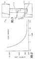
- the time period required for turn off of the power switch is controlled in accordance with a time-current curve as shown in FIGURE 2, as is well known, so that the waiting period is decreased according to a predetermined function as the amount of overload increases.
- the status of the system can be provided remotely by placing such status on the status output from the I/O.
- a signal is provided by the control logic on the trip output therefrom to indicate that power has been cut off at a remote location.
- the system can be designed to permit the power switch to be reclosed when the signal provided by the ETS indicates a current to the load is the permissible (less than the predetermined) range.
- the ETS 1 comprises a resistive element 3 of predetermined resistance as shown in FIGURE 3.
- a first temperature sensor or transducer 5 is disposed on the element at the central region thereof to measure the element temperature and a second sensor or transducer 7 is disposed adjacent the element and in close proximity thereto to measure the ambient temperature.
- the element 3 is shown mounted on heat sink studs 9 and 11 at which locations the element 3 is coupled to the line and the load. In this manner, the temperature differential between ambient and the element can be determined.
- the temperature differential is determined by providing a signal indicative of measured temperature from each sensor along the lines 13 and 15 to a comparator (not shown) which provides an output voltage indicative thereof.
- the difference signal is utilized by the control logic to determine when an alarm condition is present as shown in FIGURE 1.
- the comparator can be a part of the control logic.
- the resistive element 3 which has a predetermined resistance, has a temperature sensor 5 thereon, the temperature sensor providing an indication of the element temperature via a signal conditioner 17, the signal conditioner then providing one of the two inputs to the comparator 19.
- the other input to the comparator 19 is a signal indicative of ambient temperature as discussed hereinabove which would be provided, for example, from the sensor 7 via lines 15 and intermediate signal conditioner (not shown).
- the voltage across the resistive element 3 is sensed, this voltage being a function of line current. This voltage is sensed by a differential voltage amplifier 21 which provides an output indicative of said voltage to an instant trip comparator 23.
- the instant trip comparator 23 compares the output from the comparator 21 with a reference signal to provide the trip signal when the output therefrom reaches some predetermined value.
- the ETS per se can take many forms.
- a preferred form, as shown in FIGURE 5, includes a steatite substrate 25 having the conductive wire formed thereon of palladium/silver by silk screening. Current through the conductive wire 5 causes heating of the substrate 25. Thick film thermistors 5 and 7 are also formed on the substrate by silk screening of nickel, though other materials (PTC/NTC) are acceptable, thermistor 5 immediately next to the conductive wire 3 and thermistor 7 at a predetermined distance from the conductive wire. The temperature difference between the two thermistor locations results in different resistances of the thermistors 5 and 7 which provides an indication of the current in the conductor in the manner discussed hereinabove. Proper sizing of the substrate 25 and the conductive wire 3 and proper location of the thermistors 5 and 7 permits a variety of current/time/temperature characteristics to be utilized.
- a further ETS embodiment, as shown in FIGURE 6, is formed by providing a shunt metal (stamping) 27, preferably of electrically conductive manganin, a copper-nickel-manganese alloy.
- a separator layer of electrically insulating material 29, preferably Kapton, a polyimide, is deposited over the shunt metal layer 27
- a grid pattern 31, preferably of nickel, which displays a substantially linear temperature coefficient of resistance, is then deposited over the separator layer 29 to form resistive temperature devices (RTDs).
- a second electrically insulating layer 33, preferably of Kapton, is then deposited over the grid layer 31.
- line current passes between the shunt terminals 35 and 37 and along the shunt layer 27 to provide heat in proportion to the current passing therethrough.
- This heat is sensed by the RTDs 31 which are spaced over the shunt 27 and provide a signal indicative of the current passing through the shunt in the same manner as discussed hereinabove.
Landscapes
- Emergency Protection Circuit Devices (AREA)
- Fuses (AREA)
- Fire-Detection Mechanisms (AREA)
- Testing Or Calibration Of Command Recording Devices (AREA)
Claims (13)
- Schaltung mit
einer Widerstandseinrichtung (3) zum Anschluß in einem Strompfad von einer elektrischen Quelle zu einer Last,
einem ersten elektrothermischen Sensor (5) mit zwei Anschlüssen, der an die Widerstandseinrichtung angrenzend liegt,
einem zweiten elektrothermischen Sensor (7) mit zwei Anschlüssen, der von der Widerstandseinrichtung entfernt liegt, sowie
einer Einrichtung, die so mit dem ersten und dem zweiten elektrothermischen Sensor verbunden ist, daß sie auf die Temperaturen dieser Sensoren anspricht, um ein Ausgangssignal zu liefern, das von der Differenz zwischen diesen Temperaturen abhängt,
dadurch gekennzeichnet, daß
die mit dem ersten und dem zweiten elektrothermischen Sensor verbundene Einrichtung aufweist:
einen ersten Signalbildner (17), der mit den beiden Anschlüssen des ersten elektrothermischen Sensors (5) so verbunden ist, daß er auf eine elektrische Eigenschaft des ersten Sensors anspricht, um ein elektrisches Signal zu liefern, das die Temperatur des ersten Sensors angibt,
einen zweiten Signalbildner, der mit den beiden Anschlüssen des zweiten elektrothermischen Sensors (7) so verbunden ist, daß er auf eine elektrische Eigenschaft des Sensors anspricht, um ein elektrisches Signal zu liefern, das die Temperatur des zweiten Sensors angibt, sowie
eine Differenzeinrichtung (19), die auf die elektrischen Signale von dem ersten (17) und dem zweiten Signalbildner anspricht, um das Ausgangssignal zu erzeugen. - Schaltung nach Anspruch 1, bei welcher die Widerstandseinrichtung (3) und der erste (5) und der zweite (7) elektrothermische Sensor jeweils auf dem gleichen Keramiksubstrat (25) gebildet sind.
- Schaltung nach Anspruch 2, bei welcher die Widerstandseinrichtung (8) und der erste (5) und der zweite elektrothermische Sensor (7) auf dem Substrat aufgebrachte Schichten sind.
- Schaltung nach Anspruch 1, bei welcher der erste elektrothermische Sensor (29, 31, 33) in innigem Kontakt mit der Widerstandseinrichtung (27) angeordnet ist.
- Schaltung nach Anspruch 4, bei welcher die Widerstandseinrichtung eine Schicht (27) aus elektrisch leitendem Material mit einem vorbestimmten Widerstand aufweist und der erste elektrothermische Sensor eine erste elektrisch isolierende Schicht (29), ein auf der Isolierschicht (29) angeordnetes Gitter (31) aus auf Wärme ansprechendem Material mit einem im wesentlichen linearen Widerstandstemperaturkoeffizienten sowie eine über dem Gitter (31) angeordnete zweite elektrisch isolierende Schicht (33) aufweist.
- Schaltung nach Anspruch 5, bei welcher die Schicht (31) aus elektrisch leitendem Material zwei an entgegengesetzten Enden angeordnete Anschlüsse (35, 37) aufweist.
- Schaltung nach Anspruch 5 oder 6, bei welcher das Gitter (31) aus Nickel gebildet ist.
- Schaltung nach einem der Ansprüche 5 bis 7, bei welcher wenigstens eine der elektrisch isolierenden Schichten (29, 33) aus Polyimid gebildet ist.
- Schutzschaltung mit
einer Schaltung nach einem der Ansprüche 1 bis 8 sowie
einer Schalteinrichtung, die in den Strompfad geschaltet ist und so arbeitet, daß sie den Strompfad in Reaktion auf das Ausgangssignal unterbricht. - Schaltung nach einem der Ansprüche 1 bis 8 mit
einer Sofortauslöseeinrichtung (21, 23) mit zwei Eingängen, die jeweils mit einem der entgegengesetzten Enden der Widerstandseinrichtung (3) verbunden sind, so daß sie auf die Spannung an der Widerstandseinrichtung anspricht, um ein Sofortauslöseausgangssignal zu erzeugen, wenn die Spannung an der Widerstandseinrichtung einen vorbestimmten Wert überschreitet. - Schutzschaltung mit
einer Schaltung nach Anspruch 10 und
einer Schalteinrichtung, die so geschaltet ist, daß sie den Strompfad in Reaktion auf das Ausgangssignal von der Differenzeinrichtung oder das Sofortauslöseausgangssignal unterbricht. - Schutzschaltung nach Anspruch 9 oder 11, bei welcher die Schalteinrichtung ein Leistungs-FET ist.
- Schutzschaltung nach einem der Ansprüche 9, 11 und 12, die ferner eine Steuerlogikeinrichtung aufweist, die auf das Ausgangssignal und auf ein externes Signal anspricht, um den Betrieb der Schalteinrichtung zu steuern.
Applications Claiming Priority (2)
| Application Number | Priority Date | Filing Date | Title |
|---|---|---|---|
| US224153 | 1988-07-26 | ||
| US07/224,153 US4866559A (en) | 1988-07-26 | 1988-07-26 | Solid state circuit protector |
Publications (3)
| Publication Number | Publication Date |
|---|---|
| EP0352987A2 EP0352987A2 (de) | 1990-01-31 |
| EP0352987A3 EP0352987A3 (de) | 1991-07-10 |
| EP0352987B1 true EP0352987B1 (de) | 1994-04-13 |
Family
ID=22839485
Family Applications (1)
| Application Number | Title | Priority Date | Filing Date |
|---|---|---|---|
| EP19890307456 Expired - Lifetime EP0352987B1 (de) | 1988-07-26 | 1989-07-21 | Festkörperschaltungs-Schutzvorrichtung |
Country Status (4)
| Country | Link |
|---|---|
| US (1) | US4866559A (de) |
| EP (1) | EP0352987B1 (de) |
| JP (1) | JPH0284009A (de) |
| DE (1) | DE68914536T2 (de) |
Families Citing this family (18)
| Publication number | Priority date | Publication date | Assignee | Title |
|---|---|---|---|---|
| US5057811A (en) * | 1988-12-22 | 1991-10-15 | Texas Instruments Incorporated | Electrothermal sensor |
| JP2811872B2 (ja) * | 1990-02-26 | 1998-10-15 | 富士電機株式会社 | 半導体装置の保護回路 |
| FR2671917B1 (fr) * | 1991-02-21 | 1996-10-04 | Cgae Satelem | Systeme pour la commande de l'alimentation en energie electrique et la protection d'un dispositif recepteur electrique. |
| US5223790A (en) * | 1991-05-10 | 1993-06-29 | Metricom, Inc. | Current sensor using current transformer with sintered primary |
| US5132868A (en) * | 1991-05-23 | 1992-07-21 | The United States Of America As Represented By The Secretary Of The Navy | Over-heating protective circuit |
| US5723915A (en) * | 1992-12-04 | 1998-03-03 | Texas Instruments Incorporated | Solid state power controller |
| US5444590A (en) * | 1992-12-04 | 1995-08-22 | Texas Instruments Incorporated | Solid state power controller with power switch protection apparatus |
| FR2702084B1 (fr) * | 1993-02-22 | 1996-05-03 | Telemecanique | Dispositif de protection électronique d'une charge. |
| US6125024A (en) * | 1993-06-03 | 2000-09-26 | Texas Instruments Incorporated | Externally programmable solid state power controller with power switch protection apparatus and method for making |
| US5546262A (en) * | 1993-09-01 | 1996-08-13 | Schneider Electric Sa | Electronic protection device |
| US5550526A (en) * | 1994-12-27 | 1996-08-27 | Lucent Technologies Inc. | Thermal detection elements with heater |
| US5723846A (en) * | 1995-07-11 | 1998-03-03 | Technology Licensing Corporation | Multiprobe intelligent diagnostic system for food-processing apparatus |
| GB9813982D0 (en) * | 1998-06-30 | 1998-08-26 | Mem Limited | Residual current detection device |
| GB0000067D0 (en) * | 2000-01-06 | 2000-02-23 | Delta Electrical Limited | Current detector and current measurement apparatus including such detector with temparature compensation |
| US7400482B2 (en) * | 2006-01-17 | 2008-07-15 | Eaton Corporation | Circuit breaker and method for sensing current indirectly from bimetal voltage and determining bimetal temperature and corrected temperature dependent bimetal resistance |
| US20080214512A1 (en) * | 2007-03-01 | 2008-09-04 | Christian Seitz | Pharmaceutical preparation containing a gestagen, and kit and method for treating endometriosis using the preparation |
| JP6383536B2 (ja) * | 2013-12-09 | 2018-08-29 | カルソニックカンセイ株式会社 | 車両空調用安全装置、及びその制御方法 |
| CN109961990B (zh) * | 2017-12-22 | 2024-11-12 | 南京萨特科技发展有限公司 | 一种保护元件及保护模块 |
Family Cites Families (7)
| Publication number | Priority date | Publication date | Assignee | Title |
|---|---|---|---|---|
| GB838298A (en) * | 1956-06-21 | 1960-06-22 | Reyrolle A & Co Ltd | Improvements in or relating to electric protective relay devices |
| US4698655A (en) * | 1983-09-23 | 1987-10-06 | Motorola, Inc. | Overvoltage and overtemperature protection circuit |
| US4547826A (en) * | 1983-11-30 | 1985-10-15 | General Electric Company | Generalized real-time thermal model |
| EP0197707A2 (de) * | 1985-04-01 | 1986-10-15 | Motorola, Inc. | Elektronischer Abschalter |
| FR2581807B1 (fr) * | 1985-05-13 | 1988-06-03 | Crouzet Sa | Dispositif de protection thermique |
| FR2586489B1 (fr) * | 1985-08-23 | 1988-02-26 | Telemecanique Electrique | Dispositif de determination numerique et de sauvegarde d'une image thermique |
| JPH0683042B2 (ja) * | 1986-03-31 | 1994-10-19 | 株式会社東芝 | 出力ドライバ回路 |
-
1988
- 1988-07-26 US US07/224,153 patent/US4866559A/en not_active Expired - Fee Related
-
1989
- 1989-07-21 DE DE68914536T patent/DE68914536T2/de not_active Expired - Fee Related
- 1989-07-21 EP EP19890307456 patent/EP0352987B1/de not_active Expired - Lifetime
- 1989-07-25 JP JP1192447A patent/JPH0284009A/ja active Pending
Also Published As
| Publication number | Publication date |
|---|---|
| EP0352987A3 (de) | 1991-07-10 |
| US4866559A (en) | 1989-09-12 |
| DE68914536D1 (de) | 1994-05-19 |
| JPH0284009A (ja) | 1990-03-26 |
| EP0352987A2 (de) | 1990-01-31 |
| DE68914536T2 (de) | 1994-07-28 |
Similar Documents
| Publication | Publication Date | Title |
|---|---|---|
| US5140394A (en) | Electrothermal sensor apparatus | |
| EP0352987B1 (de) | Festkörperschaltungs-Schutzvorrichtung | |
| US4546238A (en) | Circuit arrangement for temperature control of an electric heating element | |
| EP2058832B1 (de) | Trennschalter, Auslösungsanordnung, Bimetall-Kompensationschaltung mit Kompensation für Bimettall-Temperaturkoeffizienten | |
| US5757261A (en) | Temperature controller having a Bimetallic element and plural heating components | |
| KR101904578B1 (ko) | 부하를 보호하기 위한 장치 및 방법 | |
| CA1317655C (en) | Temperature sensing circuit | |
| US6141198A (en) | Solid state overload relay | |
| IE781888L (en) | A heating circuit | |
| US4092520A (en) | Leakage current thermostat | |
| US4851954A (en) | Monitoring apparatus for monitoring temperature in a circuit arrangement | |
| US8173938B2 (en) | Controller for a heating cable | |
| US5546262A (en) | Electronic protection device | |
| JPH079782B2 (ja) | 過熱防止装置付回路遮断器 | |
| US4882574A (en) | Two-resistor ice detector | |
| US4994651A (en) | Solid state temperature dependent direct voltage interrupter for a heater circuit | |
| EP0113463B1 (de) | Elektrischer Detektor zur Erfassung der einem ohmschen Verbraucher zugeführten Energie | |
| JPH0832361A (ja) | 保護装置付き増幅回路 | |
| US6839212B2 (en) | Bus bar thermal detection | |
| US4538199A (en) | Electrothermal wire responsive miniature precision current sensor | |
| US9520707B2 (en) | Device for protecting a user | |
| EP0217620B1 (de) | Temperatursensor | |
| US5115188A (en) | Resistance sensor and switch | |
| JPH1197215A (ja) | バリスタおよびバリスタ内蔵電源装置 | |
| US4800292A (en) | Temperature sensing circuit |
Legal Events
| Date | Code | Title | Description |
|---|---|---|---|
| PUAI | Public reference made under article 153(3) epc to a published international application that has entered the european phase |
Free format text: ORIGINAL CODE: 0009012 |
|
| AK | Designated contracting states |
Kind code of ref document: A2 Designated state(s): DE FR GB IT NL |
|
| PUAL | Search report despatched |
Free format text: ORIGINAL CODE: 0009013 |
|
| AK | Designated contracting states |
Kind code of ref document: A3 Designated state(s): DE FR GB IT NL |
|
| RHK1 | Main classification (correction) |
Ipc: H02H 5/04 |
|
| 17P | Request for examination filed |
Effective date: 19911119 |
|
| 17Q | First examination report despatched |
Effective date: 19930308 |
|
| GRAA | (expected) grant |
Free format text: ORIGINAL CODE: 0009210 |
|
| ITF | It: translation for a ep patent filed | ||
| AK | Designated contracting states |
Kind code of ref document: B1 Designated state(s): DE FR GB IT NL |
|
| REF | Corresponds to: |
Ref document number: 68914536 Country of ref document: DE Date of ref document: 19940519 |
|
| ITTA | It: last paid annual fee | ||
| ET | Fr: translation filed | ||
| PLBE | No opposition filed within time limit |
Free format text: ORIGINAL CODE: 0009261 |
|
| STAA | Information on the status of an ep patent application or granted ep patent |
Free format text: STATUS: NO OPPOSITION FILED WITHIN TIME LIMIT |
|
| 26N | No opposition filed | ||
| PGFP | Annual fee paid to national office [announced via postgrant information from national office to epo] |
Ref country code: GB Payment date: 20010614 Year of fee payment: 13 |
|
| PGFP | Annual fee paid to national office [announced via postgrant information from national office to epo] |
Ref country code: NL Payment date: 20010618 Year of fee payment: 13 |
|
| PGFP | Annual fee paid to national office [announced via postgrant information from national office to epo] |
Ref country code: FR Payment date: 20010702 Year of fee payment: 13 |
|
| PGFP | Annual fee paid to national office [announced via postgrant information from national office to epo] |
Ref country code: DE Payment date: 20010731 Year of fee payment: 13 |
|
| REG | Reference to a national code |
Ref country code: GB Ref legal event code: IF02 |
|
| PG25 | Lapsed in a contracting state [announced via postgrant information from national office to epo] |
Ref country code: GB Free format text: LAPSE BECAUSE OF NON-PAYMENT OF DUE FEES Effective date: 20020721 |
|
| PG25 | Lapsed in a contracting state [announced via postgrant information from national office to epo] |
Ref country code: NL Free format text: LAPSE BECAUSE OF NON-PAYMENT OF DUE FEES Effective date: 20030201 Ref country code: DE Free format text: LAPSE BECAUSE OF NON-PAYMENT OF DUE FEES Effective date: 20030201 |
|
| GBPC | Gb: european patent ceased through non-payment of renewal fee |
Effective date: 20020721 |
|
| PG25 | Lapsed in a contracting state [announced via postgrant information from national office to epo] |
Ref country code: FR Free format text: LAPSE BECAUSE OF NON-PAYMENT OF DUE FEES Effective date: 20030331 |
|
| NLV4 | Nl: lapsed or anulled due to non-payment of the annual fee |
Effective date: 20030201 |
|
| REG | Reference to a national code |
Ref country code: FR Ref legal event code: ST |
|
| PG25 | Lapsed in a contracting state [announced via postgrant information from national office to epo] |
Ref country code: IT Free format text: LAPSE BECAUSE OF NON-PAYMENT OF DUE FEES;WARNING: LAPSES OF ITALIAN PATENTS WITH EFFECTIVE DATE BEFORE 2007 MAY HAVE OCCURRED AT ANY TIME BEFORE 2007. THE CORRECT EFFECTIVE DATE MAY BE DIFFERENT FROM THE ONE RECORDED. Effective date: 20050721 |