EP0353423B1 - Hétérostructures épitaxiales désadaptées indéformées et libres de défauts; procédé pour leur fabrication - Google Patents
Hétérostructures épitaxiales désadaptées indéformées et libres de défauts; procédé pour leur fabrication Download PDFInfo
- Publication number
- EP0353423B1 EP0353423B1 EP89110424A EP89110424A EP0353423B1 EP 0353423 B1 EP0353423 B1 EP 0353423B1 EP 89110424 A EP89110424 A EP 89110424A EP 89110424 A EP89110424 A EP 89110424A EP 0353423 B1 EP0353423 B1 EP 0353423B1
- Authority
- EP
- European Patent Office
- Prior art keywords
- semiconductor material
- heterostructure
- lattice constant
- intermediate layer
- layer
- Prior art date
- Legal status (The legal status is an assumption and is not a legal conclusion. Google has not performed a legal analysis and makes no representation as to the accuracy of the status listed.)
- Expired - Lifetime
Links
Images


Classifications
-
- H—ELECTRICITY
- H10—SEMICONDUCTOR DEVICES; ELECTRIC SOLID-STATE DEVICES NOT OTHERWISE PROVIDED FOR
- H10P—GENERIC PROCESSES OR APPARATUS FOR THE MANUFACTURE OR TREATMENT OF DEVICES COVERED BY CLASS H10
- H10P14/00—Formation of materials, e.g. in the shape of layers or pillars
- H10P14/20—Formation of materials, e.g. in the shape of layers or pillars of semiconductor materials
- H10P14/29—Formation of materials, e.g. in the shape of layers or pillars of semiconductor materials characterised by the substrates
- H10P14/2901—Materials
- H10P14/2907—Materials being Group IIIA-VA materials
- H10P14/2911—Arsenides
-
- H—ELECTRICITY
- H10—SEMICONDUCTOR DEVICES; ELECTRIC SOLID-STATE DEVICES NOT OTHERWISE PROVIDED FOR
- H10P—GENERIC PROCESSES OR APPARATUS FOR THE MANUFACTURE OR TREATMENT OF DEVICES COVERED BY CLASS H10
- H10P14/00—Formation of materials, e.g. in the shape of layers or pillars
- H10P14/20—Formation of materials, e.g. in the shape of layers or pillars of semiconductor materials
- H10P14/32—Formation of materials, e.g. in the shape of layers or pillars of semiconductor materials characterised by intermediate layers between substrates and deposited layers
- H10P14/3202—Materials thereof
- H10P14/3214—Materials thereof being Group IIIA-VA semiconductors
- H10P14/3221—Arsenides
-
- H—ELECTRICITY
- H10—SEMICONDUCTOR DEVICES; ELECTRIC SOLID-STATE DEVICES NOT OTHERWISE PROVIDED FOR
- H10P—GENERIC PROCESSES OR APPARATUS FOR THE MANUFACTURE OR TREATMENT OF DEVICES COVERED BY CLASS H10
- H10P14/00—Formation of materials, e.g. in the shape of layers or pillars
- H10P14/20—Formation of materials, e.g. in the shape of layers or pillars of semiconductor materials
- H10P14/34—Deposited materials, e.g. layers
- H10P14/3402—Deposited materials, e.g. layers characterised by the chemical composition
- H10P14/3414—Deposited materials, e.g. layers characterised by the chemical composition being group IIIA-VIA materials
- H10P14/3421—Arsenides
-
- Y—GENERAL TAGGING OF NEW TECHNOLOGICAL DEVELOPMENTS; GENERAL TAGGING OF CROSS-SECTIONAL TECHNOLOGIES SPANNING OVER SEVERAL SECTIONS OF THE IPC; TECHNICAL SUBJECTS COVERED BY FORMER USPC CROSS-REFERENCE ART COLLECTIONS [XRACs] AND DIGESTS
- Y10—TECHNICAL SUBJECTS COVERED BY FORMER USPC
- Y10S—TECHNICAL SUBJECTS COVERED BY FORMER USPC CROSS-REFERENCE ART COLLECTIONS [XRACs] AND DIGESTS
- Y10S148/00—Metal treatment
- Y10S148/072—Heterojunctions
-
- Y—GENERAL TAGGING OF NEW TECHNOLOGICAL DEVELOPMENTS; GENERAL TAGGING OF CROSS-SECTIONAL TECHNOLOGIES SPANNING OVER SEVERAL SECTIONS OF THE IPC; TECHNICAL SUBJECTS COVERED BY FORMER USPC CROSS-REFERENCE ART COLLECTIONS [XRACs] AND DIGESTS
- Y10—TECHNICAL SUBJECTS COVERED BY FORMER USPC
- Y10S—TECHNICAL SUBJECTS COVERED BY FORMER USPC CROSS-REFERENCE ART COLLECTIONS [XRACs] AND DIGESTS
- Y10S148/00—Metal treatment
- Y10S148/097—Lattice strain and defects
-
- Y—GENERAL TAGGING OF NEW TECHNOLOGICAL DEVELOPMENTS; GENERAL TAGGING OF CROSS-SECTIONAL TECHNOLOGIES SPANNING OVER SEVERAL SECTIONS OF THE IPC; TECHNICAL SUBJECTS COVERED BY FORMER USPC CROSS-REFERENCE ART COLLECTIONS [XRACs] AND DIGESTS
- Y10—TECHNICAL SUBJECTS COVERED BY FORMER USPC
- Y10S—TECHNICAL SUBJECTS COVERED BY FORMER USPC CROSS-REFERENCE ART COLLECTIONS [XRACs] AND DIGESTS
- Y10S438/00—Semiconductor device manufacturing: process
- Y10S438/933—Germanium or silicon or Ge-Si on III-V
-
- Y—GENERAL TAGGING OF NEW TECHNOLOGICAL DEVELOPMENTS; GENERAL TAGGING OF CROSS-SECTIONAL TECHNOLOGIES SPANNING OVER SEVERAL SECTIONS OF THE IPC; TECHNICAL SUBJECTS COVERED BY FORMER USPC CROSS-REFERENCE ART COLLECTIONS [XRACs] AND DIGESTS
- Y10—TECHNICAL SUBJECTS COVERED BY FORMER USPC
- Y10S—TECHNICAL SUBJECTS COVERED BY FORMER USPC CROSS-REFERENCE ART COLLECTIONS [XRACs] AND DIGESTS
- Y10S438/00—Semiconductor device manufacturing: process
- Y10S438/938—Lattice strain control or utilization
Definitions
- This invention relates to lattice mismatched heterostructures and to methods for epitaxially growing layers of crystalline materials on a mismatched substrate.
- the interface between non lattice matched materials has proved to be a source of structural defects with electronic properties which greatly limit that potential utility.
- the defects include edge and 60 degree misfit dislocations, and 60 degree threading dislocations.
- misfit dislocation means a dislocation, or a portion of the dislocation line, that lies parallel to the plane of the substrate, and thus can accommodate part of the lattice mismatch between the substrate and an epitaxial layer.
- threading dislocation strictly refers to dislocations originating from the substrate and propagating into the epitaxial layers above it, colloquially it refers to any dislocations inclined to the plane of the substrate and propagating through the epitaxial layer at some non-normal angle to the growth axis.
- the term “threading dislocation” will be used in its colloquial sense hereinafter. 60 degree dislocations are introduced by glide, and therefore they can have both threading and misfit segments. Edge dislocations can be formed by the reaction of two 60 degree dislocations, and therefore any unreacted segments can act as 60 degree dislocations. Edge dislocations by themselves are sessile and do not glide. Edge dislocations have been reported (Petroff et al., J. Micro.
- Edge dislocations are "composed of" two 60 degree dislocations, and therefore an edge dislocation relieves twice the mismatch compared to a single 60 degree dislocation. Edge dislocations, being less dense for a given relief or misfit, and being sessile, are preferrable to 60 degree dislocations. 60 degree misfit dislocations are electrically active, but because they lie in or near the mismatched interface, they are spatially isolated from successive layers. Various electronic isolation techniques, such as p-n junction isolation, can be used to further reduce their effect.
- Threading dislocations are known to be associated with radiative recombination, and because the dislocations thread through the device layers this adversely affects the performance of optical and electrical devices fabricated from such systems.
- one prior art approach utilizes the pseudomorphic growth of non lattice matched materials.
- initial epitaxial growth of a lattice mismatched material upon a substrate occurs two-dimensionally, with the epilayer conforming to the in-plane lattice structure of the substrate and with the mismatch accommodated by elastic strain.
- This growth is termed commensurate because it is growing with the lattice constant of the substrate, rather than the unstrained bulk lattice constant of the epitaxial layer material.
- the commensurate growth is pseudomorphic as long as the layer thickness is below a critical thickness (which for a mismatch of about 1-5% is about 1-100 nm) which defines the strain energy for which the introduction of dislocations becomes energetically favored.
- a critical thickness which for a mismatch of about 1-5% is about 1-100 nm
- Many lattice mismatched devices have been made in which the strained layer thickness is kept below the critical thickness.
- many electronic or optoelectronic devices require non lattice matched layers with thicknesses exceeding the limits of pseudomorphism, or with too much mismatch for the attraction between the film and the substrate to allow 2-dimensional nucleation.
- a second prior art approach to fabricating heterojunctions of lattice mismatched materials utilizes a strained layer superlattice technique in which layers are alternately placed under compressive and tensile strain, but in which the average lattice constant is matched to the substrate. While the superlattice can be nearly free of misfit dislocations, the material selection is still limited by the need to match the average lattice constant of the superlattice to the substrate, the need to keep the individual layer's thicknesses below their critical thicknesses, and the need to restrict mismatch to maintain 2-D growth.
- the desired lattice constant can be obtained by compositional step-grading, by growing several layers above their critical thicknesses, limiting the change in lattice constant at each interface to less than about 1.5% (within the InGaAs system).
- the grading from the lattice constant of the substrate material to the lattice constant of the final layer is in steps that are small enough to allow reliable 2-dimensional growth throughout the growth process.
- the drawback of this technique is that the multilayer combination contains enough total strain energy to introduce additional misfit and threading dislocations, with only kinetic limitations to their eventual introduction.
- the structure contains a significant number of undesired threading dislocations, and is predisposed to the addition of more over time, causing degraded electrical and optical properties and unreliable operation.
- the defects so formed are photo-electrically active and are also strong scatterers so that the transition material must be separated from active regions of the subsequent heterostructure by large buffer layers and/or drift fields.
- European Patent Application EP-A-0 232 082 discloses a method for epitaxial growth of semiconductor materials, such as a group III-V semiconductor, epitaxially grown on silicon or germanium while accommodating lattice mismatch in a manner that results in improved material quality.
- the method involves forming a single crystalline silicon or germanium substrate having a crystallographic surface tilted in the ⁇ 001> direction and epitaxially depositing a different single crystalline semiconductor material over the surface to obtain a layer of the semiconductor material.
- the present invention is directed to heterojunction structures and to a method for making heterojunctions between various materials of interest which have a large mismatch in their unstrained bulk lattice constants. This is accomplished by interposing a thin intermediate layer between a substrate of a first semiconductor material and an epitaxially grown upper layer of a second semiconductor material having mismatched lattice constants.
- the intermediate layer is comprised of a third semiconductor material having an unstrained or bulk lattice constant with a greater mismatch with the bulk lattice constant of the substrate than the mismatch between the substrate and the upper layer. It is known that for large mismatches, there will be a growth period in which the layer is growing with a partially relaxed lattice constant.
- the amount of mismatch necessary that will result in the partially relaxed lattice constant is system and growth dependent.
- the inventors have determined that the mismatch must be about 2.5% or greater.
- the inventors have also determined that during this growth period, the strain is partially relieved substantially due to a planar array of edge type dislocations introduced during a short period of growth when the film becomes 3-dimensional. The array is complete enough that a minimum of threading dislocations are created when the layer coalesces back to two dimensions upon this partial relief of strain and a minimum of additional growth.
- the growth of the intermediate layer is stopped while the layer is growing in an essentially 2-dimensional mode with the strain partially relieved by the edge type dislocations.
- the growth of the intermediate layer is interrupted before the layer reaches a second critical thickness determined by the residual strain, in which the strain would be further relieved by 60 degree misfit dislocations with threading segments.
- Epitaxial growth of the upper layer upon the intermediate layer is then commenced.
- the bulk lattice constant of the upper layer is approximately equal to the partially relaxed in-plane lattice constant of the intermediate layer. Therefore, the upper layer is unstrained, and it is stable against the introduction of additional defects, as if grown on a lattice-matched substrate.
- planar array of edge type dislocations is localized near the interface and unable to migrate into the epilayer, and thus should cause no effect on the properties of the adjacent layers.
- the necessity of including large buffer layers or drift fields within the heterostructure in order to separate active areas from the plastically deformed region is potentially eliminated by the present invention.
- MBE molecular beam epitaxy
- the intermediate layer of In 0.9 Ga 0.1 As is between 3-10 nm thick.
- approximately 80% of the mismatch in the lattice constants is accommodated by the planar array of edge dislocations that forms at the In 0.9 Ga 0.1 As-GaAs interface.
- Photoelectrically active threading dislocations have not formed in large numbers.
- two intermediate layers are grown.
- MBE is used to grow the In 0.9 Ga 0.1 As intermediate layer about 10 nm thick, where it has relaxed about 80% of its original 6.3% misfit by incorporating edge dislocations at or near its interface with the GaAs substrate during a 3-dimensional phase in its growth. Having coalesced into a continuous and substantially 2-dimensional film by 10 nm thickness, the layer has not exceeded the critical thickness (for the residual 1.3% lattice mismatched needed to produce additional 60 degree misfit dislocations by glide.
- the in-plane lattice constant is approximately that of unstrained In 0.72 Ga 0.28 As.
- the residual compressive strain in the In 0.9 Ga 0.1 As can be offset by growing 20 nm of In 0.63 Ga 0.37 As, which when grown with an in-plane lattice constant of In 0.72 Ga 0.28 As, has a net tensile strain that balances the net residual compressive strain energy in the 10 nm In 0.9 Ga 0.1 As layer.
- the Upper In 0.72 Ga 0.28 As layer can then be grown arbitrarily thick, nearly defect-free and unstrained, atop this substrate-double intermediate layer combination that contains little if any net strain energy. This transformation of lattice constant has been accomplished within 30 nm of growth, taking about 2 minutes at conventional MBE growth rates.
- the heterojunction structures of the invention have epitaxial layers grown on a mismatched substrate without large densities of propagating (inclined) photoelectrically active crystal defects.
- a new array of optoelectronic devices may now be fabricated using highly desirable material systems that are not lattice matched to suitable substrates. These systems include InGaAs on GaAs, Ge-Si alloys on Si, and GaAs or InGaAs on Si.
- heterostructures comprising unstrained, essentially defect-free epilayers of a first semiconductor material are grown on substrates of a second semiconductor material, in which there is a large difference between the unstrained lattice constants of the materials. This is accomplished with only a thin intermediate layer of a third semiconductor material sandwiched between the substrate and the upper epilayer.
- the unique method of fabricating the heterostructures of the invention is based, in part, on the nature of strained layer growth and its relaxation behavior.
- the inventors have determined for a large mismatch of the unstrained lattice constants, that after the initial planar pseudomorphic growth, the layer collapses into 3-dimensional island growth. During this 3-D growth, a large fraction of the strain is abruptly relieved by the introduction of a planar array of edge type dislocations. For the InGaAs/GaAs interface this occurs after about 1-2 nm of growth. As growth continues to a thickness of about 10-20 nm, the growth again becomes planar. The array of edge type dislocations is complete enough that a minimum of threading dislocations are created when the layer coalesces back to two dimensions.
- Fig. 1 shows a cross-sectional view of a prior art heterojunction structure 10 that results from the conventional growth of large mismatched materials.
- Heterostructure 10 comprises a substrate 12 of one semiconductor material with unstrained lattice constant a S , and an epitaxially grown layer 14 of a different semiconductor material with an unstrained lattice constant a L .
- the absolute value of the difference is used in equation (1) since for various materials used for layer 14 can have a bulk lattice constant either larger or smaller than a L .
- ⁇ L-S 2.5% or greater, as shown in Fig. 1, the growth of layer 14 to a thickness sufficient to allow 100% relaxation, results in the formation of both edge type misfit dislocations 15 and a high density of photoelectrically active threading dislocations 16. These defects make the heterojunction structure of Fig. 1 ineffective for many optoelectronic applications.
- the intermediate layer is formed by interrupting the growth of that layer while it is growing with the partially relaxed in-plane lattice constant.
- the inventors have determined that during the partial relaxation growth period, the strain is partially relieved substantially by a planar array of edge type dislocations without a significant number of threading dislocations.
- the growth of the upper epilayer is commenced.
- the upper epilayer has a bulk lattice constant approximately equal to the partially relaxed in-plane lattice constant of the intermediate layer and therefore, the upper epilayer will grow unstrained and defect free.
- the upper epilayer is lattice matched to the in-plane lattice constant of the partially relaxed intermediate layer but is mismatched with the substrate.
- the present invention provides a heterostructure having an epilayer with a large lattice mismatch with respect to the substrate that includes only a thin intermediate layer.
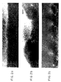
- Figures 2(a), 2(b) and 2(c) are TEM pictures of the growth of InGaAs on GaAs at various thicknesses.
- Figure 2(a) is after approximately 1 nm of growth which shows the growth as being essentially planar and pseudomorphic.
- Figure 2(b) shows the 3D island growth after approximately 5 nm.
- the presence of a small number of edge type dislocations are indicated by the letter E.
- Figure 2(c) is after 10 nm of growth showing that the growth has returned to planar.
- Substantially all of the defects are edge type dislocations with only one threading dislocation indicated by the letter T.
- the density of photoelectrically active threading dislocations is therefore very small during the partial relaxation growth period.
- the strain in the intermediate layer is partially relieved during this growth period substantially by a planar array of edge type dislocations.
- a heterostructure 20 of the invention includes a substrate 22 of a first semiconductor material with a bulk lattice constant a S .
- the heterostructure 20 also includes an upper epitaxially grown layer 24 of a second semiconductor material with a bulk lattice constant a L2 Interposed between layers 24 and 22 is an epitaxially grown layer 26 of a third semiconductor material.
- the intermediate layer 26 has a bulk lattice constant a L .
- the epitaxial growth of layer 26 begins pseudomorphically and strained to the lattice constant of the substrate, a S .
- the strain becomes partially relieved by the edge type dislocations and layer 26 then grows with a partially relaxed in-plane lattice constant, a L1 .
- the layer 26 continues to grow with the partially relaxed in-plane lattice constant for a predetermined thickness depending on growth conditions and the material used.
- the growth of layer 26 is halted while it is growing at the a L1 lattice constant.
- the bulk lattice mismatch between layers 26 and 22 for the InGaAs/GaAs system should be greater than the 2.5% and typically will be in the range 3% to 7.5%.
- the strain, at the time growth is interrupted for InAs is approximately 80% relieved, and therefore, the ⁇ L1-S for structure 20 will be approximately 80% of ⁇ L-S .
- the partial relaxation value, ⁇ L1 for the InGaAs 80% relaxed in-plane lattice constant is approximately 1-2%.
- the materials are selected for layers 24 and 26 so that the bulk lattice constant of layer 24, a L2 , is approximately equal to the partially relaxed lattice constant of layer 26, a L1 .
- layer 24 grows lattice matched with layer 26 and is therefore, unstrained and defect free.
- the absolute values are used in the above definition of ⁇ L1-S because the lattice constant a L1 can be either larger or smaller than a S .
- the only requirement is that the bulk unstrained lattice constant of layer 26, a L , be at least 2.5% different than a S .
- the bulk lattice constant of layer 24, a L1 will always be between the a L and a S values, whether a L is larger or smaller than a S .
- the thickness of layer 26 must be less than the second critical thickness, which is the thickness above which the left over strain is relieved by 60 degree type threading dislocations.
- the thickness at which InGaAs is growing with the 80% relaxed in-plane lattice constant is between 3 and 10 nm.
- a layer of In 0.72 Ga 0.28 As has been epitaxially grown by MBE on a GaAs substrate through the inclusion of an intermediate layer of In 0.9 Ga 0.1 As of less than 10 nm in thickness.
- the In 0.9 Ga 0.1 As layer contained the stabilized and localized damage necessary to relieve the strain in the system. Moreover, the damage consists primarily of defects confined to the interface plane which cause little or no effect on the optical properties or mobility in adjacent layers. Therefore, it is not necessary to include large buffer layers or drift fields within the heterostructure to separate the active carriers from the damaged region.
- Another system comprises an intermediate layer of GaInAs upon a substrate of GaAs.
- the upper epilayer may also comprise GaInAs, as long as the In concentration in the intermediate layer is greater than in the upper layer.
- AlInAs can also be used as an upper epilayer on the GaInAs/GaAs substrate ensemble.
- an intermediate layer of AlInAs upon a substrate of GaAs is used.
- the upper epilayer may comprise AlInAs as long as the In concentration in the intermediate layer is greater than in the upper layer.
- GaInAs can also be used as an upper epilayer on the AlInAs/GaAs substrate ensemble.
- a further system comprises a layer of InAs interposed between a GaAs substrate and an upper layer of In 0.8 Ga 0.2 As.
- a gradual relaxation of InAs on GaAs occurred on a GaAs substrate having a (100) crystallographic configuration.
- high growth temperature and low As4/In ratio may be the preferred conditions for growing the intermediate layer of the invention. It is known that such conditions provide better surface diffusion and high mobility which also is desirable.
- two intermediate layers are grown.
- MBE is used to grow an In 0.9 Ga 0.1 As intermediate layer 30 about 10 nm thick, where it has relaxed about 80% of its original 6.3% misfit by incorporating edge dislocations 32 at or near its interface with a GaAs substrate 34 during a 3-dimensional phase in its growth.
- the In 0.9 Ga 0.1 As layer coalesces into a continuous and substantially 2-dimensional film by 10 nm thickness, and has not exceeded the critical thickness (for the residual 1.3% lattice mismatch) needed to produce additional 60 degree misfit dislocations by glide.
- the in-plane lattice constant is approximately that of unstrained In 0.72 Ga 0.28 As.
- the residual compressive strain in the In 0.9 Ga 0.1 As can be offset by growing a layer 36 of 20 nm of In 0.63 Ga 0.37 As, which when grown with an in-plane lattice constant of In 0.72 Ga 0.28 As, has a net tensile strain that balances the net residual compressive strain energy in the 10 nm In 0.9 Ga 0.1 As layer 30.
- An upper In 0.72 Ga 0.28 As layer 38 can then be grown arbitrarily thick, nearly defect-free and unstrained, atop this substrate-double intermediate layer combination that contains little if any net strain energy. This transformation of lattice constant has been accomplished with 30 nm of growth, taking about 2 minutes at convenient MBE growth rates.
Landscapes
- Recrystallisation Techniques (AREA)
- Physical Deposition Of Substances That Are Components Of Semiconductor Devices (AREA)
- Crystals, And After-Treatments Of Crystals (AREA)
Claims (19)
- Hétérostructure monocristalline comprenant :
un substrat (22) d'un premier matériau semi-conducteur ayant une structure cristalline et une première constante de réseau massique aS,
une couche supérieure d'un second matériau semi-conducteur mis à croître de manière épitaxiale (24) qui est indéformée, ayant une seconde constante de réseau massique a₁₂ différente de ladite première constante de réseau massique aS, et
une couche intermédiaire d'un troisième matériau semi-conducteur mis à croître de manière épitaxiale (26) prise en sandwich entre ledit substrat (22) et ladite couche supérieure d'un second matériau semi-conducteur (24), ladite couche intermédiaire ayant une déformation partielle à l'intérieur due à sa croissance sur ledit substrat (22) et une constante de réseau dans le plan a₁₁ partiellement libérée égale ou approximativement égale à la seconde constante de réseau massique a₁₂,
dans laquelle l'épaisseur du troisième matériau semi-conducteur (26) est inférieure à l'épaisseur à laquelle ladite déformation est en outre diminuée par des dislocations pénétrantes de type à 60 degrés. - Hétérostructure selon la revendication 1, dans laquelle la couche intermédiaire d'un troisième matériau semi-conducteur (26) possède une constante de réseau massique a₁₁ suffisamment différente de la constante de réseau massique aS du premier matériau semi-conducteur (22) de sorte qu'un pourcentage de désadaptation entre ledit matériau semi-conducteur et ladite couche intermédiaire du troisième matériau semi-conducteur (26) est au moins de 2,5 %.
- Hétérostructure selon la revendication 1, dans laquelle la constante de réseau partiellement libérée dans le plan a₁₁ est libérée à environ 80 %.
- Hétérostructure selon la revendication 1, dans laquelle la déformation du troisième matériau semi-conducteur (26) est partiellement réduite à pratiquement un réseau planaire de dislocations de type bord (15) au niveau de l'interface entre le premier matériau semi-conducteur et ladite couche intermédiaire du troisième matériau semi-conducteur.
- Hétérostructure selon une ou plusieurs des revendications précédentes 1 à 4, dans laquelle le premier matériau semiconducteur (22) est du GaAs.
- Hétérostructure selon la revendication 5, dans laquelle le second matériau semi-conducteur (24) est du InGaAs et le troisième matériau semi-conducteur (26) est du InAs.
- Hétérostructure selon la revendication 5, dans laquelle le second matériau semi-conducteur (24) est du In0,8Ga0,2As.
- Hétérostructure selon la revendication 5, dans laquelle le troisième matériau semi-conducteur comprend l'un de GaInAs et AlInAS.
- Hétérostructure selon la revendication 8, dans laquelle le second matériau semi-conducteur comprend l'un de GaInAs et AlInAS et dans laquelle la concentration de In dans le troisième matériau semi-conducteur est supérieure à la concentration de In dans le second matériau semi-conducteur.
- Hétérostructure selon la revendication 5, dans laquelle le troisième matériau semi-conducteur comprend In0,9Ga0,1As et le second matériau semi-conducteur comprend In0,72Ga0,28As.
- Hétérostructure selon une ou plusieurs des revendications précédentes 1 à 4, dans laquelle le premier matériau semiconducteur (22) est du Si.
- Hétérostructure selon la revendication 11, dans laquelle le troisième matériau semi-conducteur (26) est du GaInAs.
- Hétérostructure selon la revendication 12, dans laquelle le matériau de GaInAs est constitué de 15 à 20 % de In.
- Hétérostructure selon la revendication 12, dans laquelle le second matériau semi-conducteur comprend l'un de GaAs et GaAlAs.
- Hétérostructure selon les revendications 6 et 10, dans laquelle la couche d'un troisième matériau semi-conducteur (26) est d'une épaisseur située entre 3 et 10 nm.
- Hétérostructure selon la revendication 1, comprenant en outre une seconde couche intermédiaire d'un quatrième matériau semiconducteur prise en sandwich entre ladite couche supérieure d'un second matériau semi-conducteur et ladite couche intermédiaire d'un troisième matériau semi-conducteur, ladite seconde couche intermédiaire du quatrième matériau semi-conducteur ayant une déformation partielle à l'intérieur due à sa croissance sur ledit troisième matériau semi-conducteur et une constante de réseau dans le plan partiellement libérée quasiment égale à la seconde constante de réseau massique.
- Hétérostructure selon la revendication 16, dans laquelle la seconde couche intermédiaire du quatrième matériau semiconducteur est constituée de In0,63Ga0,37As, ladite couche intermédiaire du troisième matériau semi-conducteur est constituée de In0,9Ga0,1As, ladite couche supérieure du second matériau semi-conducteur est constituée de In0,72Ga0,28As et ledit substrat est constitué de GaAs.
- Hétérostructure selon la revendication 17, dans laquelle la couche intermédiaire du troisième matériau semi-conducteur est d'une épaisseur d'environ 10 nm et la seconde couche intermédiaire du quatrième matériau semi-conducteur est d'une épaisseur d'environ 20 nm.
- Procédé pour procurer une couche semi-conductrice exempte de déformation dans une hétérostructure monocristalline comme décrit selon une ou plusieurs des revendications précédentes 1 à 18, comprenant les étapes consistant à :
procurer un substrat (22) d'un premier matériau semi-conducteur ayant une structure cristalline et une première constante de réseau massique aS,
faire croître de manière épitaxiale une couche intermédiaire d'un troisième matériau semi-conducteur (26) sur ledit substrat (22) ayant une troisième constante de réseau massique aL différente de ladite première constante de réseau massique aS et ayant une déformation à l'intérieur due à sa croissance sur ledit substrat (22) et une constante de réseau dans le plan a₁₁ partiellement libérée, la croissance ayant lieu à une épaisseur qui est inférieure à l'épaisseur à laquelle la déformation est en outre diminuée par des dislocations pénétrantes de type 60 degrés, et
faire croître de manière épitaxiale une couche supérieure (24) d'un second matériau semi-conducteur qui est indéformée et exempte de défaut, ayant une constante de réseau a₁₂ quasiment égale à ladite constante de réseau de déformation a₁₁ partiellement libérée dans le plan.
Applications Claiming Priority (2)
| Application Number | Priority Date | Filing Date | Title |
|---|---|---|---|
| US07/227,955 US5221367A (en) | 1988-08-03 | 1988-08-03 | Strained defect-free epitaxial mismatched heterostructures and method of fabrication |
| US227955 | 1988-08-03 |
Publications (3)
| Publication Number | Publication Date |
|---|---|
| EP0353423A2 EP0353423A2 (fr) | 1990-02-07 |
| EP0353423A3 EP0353423A3 (en) | 1990-12-27 |
| EP0353423B1 true EP0353423B1 (fr) | 1995-08-23 |
Family
ID=22855139
Family Applications (1)
| Application Number | Title | Priority Date | Filing Date |
|---|---|---|---|
| EP89110424A Expired - Lifetime EP0353423B1 (fr) | 1988-08-03 | 1989-06-09 | Hétérostructures épitaxiales désadaptées indéformées et libres de défauts; procédé pour leur fabrication |
Country Status (8)
| Country | Link |
|---|---|
| US (1) | US5221367A (fr) |
| EP (1) | EP0353423B1 (fr) |
| JP (1) | JPH062640B2 (fr) |
| KR (1) | KR930006524B1 (fr) |
| CN (1) | CN1016296B (fr) |
| CA (1) | CA1330194C (fr) |
| DE (1) | DE68923920T2 (fr) |
| ES (1) | ES2075837T3 (fr) |
Cited By (1)
| Publication number | Priority date | Publication date | Assignee | Title |
|---|---|---|---|---|
| US7049627B2 (en) | 2002-08-23 | 2006-05-23 | Amberwave Systems Corporation | Semiconductor heterostructures and related methods |
Families Citing this family (58)
| Publication number | Priority date | Publication date | Assignee | Title |
|---|---|---|---|---|
| FR2675948A1 (fr) * | 1991-04-23 | 1992-10-30 | Centre Nat Rech Scient | Materiaux semi-conducteurs a structure heteroepitaxiee et contrainte controlee, leur mode d'elaboration et leurs applications. |
| EP0631299A4 (fr) * | 1993-01-13 | 1997-05-14 | Sumitomo Chemical Co | Substrat epitaxial semiconducteur. |
| US5693140A (en) * | 1993-07-30 | 1997-12-02 | Lockheed Martin Energy Systems, Inc. | Process for growing a film epitaxially upon a MgO surface |
| MXPA94009540A (es) * | 1993-07-30 | 2005-04-29 | Martin Marietta Energy Systems | Procedimiento para hacer crecer una pelicula epitaxialmente sobre una superficie de oxido, y las estructuras formadas con el procedimiento. |
| JP3274246B2 (ja) * | 1993-08-23 | 2002-04-15 | コマツ電子金属株式会社 | エピタキシャルウェーハの製造方法 |
| US5456206A (en) * | 1994-12-07 | 1995-10-10 | Electronics And Telecommunications Research Institute | Method for two-dimensional epitaxial growth of III-V compound semiconductors |
| US6184144B1 (en) * | 1997-10-10 | 2001-02-06 | Cornell Research Foundation, Inc. | Methods for growing defect-free heteroepitaxial layers |
| US6693033B2 (en) | 2000-02-10 | 2004-02-17 | Motorola, Inc. | Method of removing an amorphous oxide from a monocrystalline surface |
| US6392257B1 (en) | 2000-02-10 | 2002-05-21 | Motorola Inc. | Semiconductor structure, semiconductor device, communicating device, integrated circuit, and process for fabricating the same |
| AU2001257346A1 (en) | 2000-05-31 | 2001-12-11 | Motorola, Inc. | Semiconductor device and method for manufacturing the same |
| US6477285B1 (en) | 2000-06-30 | 2002-11-05 | Motorola, Inc. | Integrated circuits with optical signal propagation |
| US6410941B1 (en) | 2000-06-30 | 2002-06-25 | Motorola, Inc. | Reconfigurable systems using hybrid integrated circuits with optical ports |
| US6427066B1 (en) | 2000-06-30 | 2002-07-30 | Motorola, Inc. | Apparatus and method for effecting communications among a plurality of remote stations |
| US6501973B1 (en) | 2000-06-30 | 2002-12-31 | Motorola, Inc. | Apparatus and method for measuring selected physical condition of an animate subject |
| US6515316B1 (en) | 2000-07-14 | 2003-02-04 | Trw Inc. | Partially relaxed channel HEMT device |
| US6555946B1 (en) | 2000-07-24 | 2003-04-29 | Motorola, Inc. | Acoustic wave device and process for forming the same |
| WO2002009187A2 (fr) | 2000-07-24 | 2002-01-31 | Motorola, Inc. | Diodes a heterojonction tunnel et processus de fabrication de celles-ci |
| US6638838B1 (en) * | 2000-10-02 | 2003-10-28 | Motorola, Inc. | Semiconductor structure including a partially annealed layer and method of forming the same |
| US6583034B2 (en) | 2000-11-22 | 2003-06-24 | Motorola, Inc. | Semiconductor structure including a compliant substrate having a graded monocrystalline layer and methods for fabricating the structure and semiconductor devices including the structure |
| US6563118B2 (en) | 2000-12-08 | 2003-05-13 | Motorola, Inc. | Pyroelectric device on a monocrystalline semiconductor substrate and process for fabricating same |
| KR100359739B1 (ko) * | 2000-12-28 | 2002-11-09 | 한국과학기술연구원 | 이종 단결정박막의 접합 및 덧성장방법 |
| US20020096683A1 (en) | 2001-01-19 | 2002-07-25 | Motorola, Inc. | Structure and method for fabricating GaN devices utilizing the formation of a compliant substrate |
| US6673646B2 (en) | 2001-02-28 | 2004-01-06 | Motorola, Inc. | Growth of compound semiconductor structures on patterned oxide films and process for fabricating same |
| US7046719B2 (en) | 2001-03-08 | 2006-05-16 | Motorola, Inc. | Soft handoff between cellular systems employing different encoding rates |
| WO2002082551A1 (fr) | 2001-04-02 | 2002-10-17 | Motorola, Inc. | Structure de semi-conducteur a courant de fuite attenue |
| US6653166B2 (en) * | 2001-05-09 | 2003-11-25 | Nsc-Nanosemiconductor Gmbh | Semiconductor device and method of making same |
| US6784074B2 (en) * | 2001-05-09 | 2004-08-31 | Nsc-Nanosemiconductor Gmbh | Defect-free semiconductor templates for epitaxial growth and method of making same |
| US7060131B2 (en) * | 2001-05-09 | 2006-06-13 | Hrl Laboratories, Llc | Epitaxy with compliant layers of group-V species |
| US6709989B2 (en) | 2001-06-21 | 2004-03-23 | Motorola, Inc. | Method for fabricating a semiconductor structure including a metal oxide interface with silicon |
| US6992321B2 (en) | 2001-07-13 | 2006-01-31 | Motorola, Inc. | Structure and method for fabricating semiconductor structures and devices utilizing piezoelectric materials |
| US6646293B2 (en) | 2001-07-18 | 2003-11-11 | Motorola, Inc. | Structure for fabricating high electron mobility transistors utilizing the formation of complaint substrates |
| US6693298B2 (en) | 2001-07-20 | 2004-02-17 | Motorola, Inc. | Structure and method for fabricating epitaxial semiconductor on insulator (SOI) structures and devices utilizing the formation of a compliant substrate for materials used to form same |
| US7019332B2 (en) | 2001-07-20 | 2006-03-28 | Freescale Semiconductor, Inc. | Fabrication of a wavelength locker within a semiconductor structure |
| US6472694B1 (en) | 2001-07-23 | 2002-10-29 | Motorola, Inc. | Microprocessor structure having a compound semiconductor layer |
| US6855992B2 (en) | 2001-07-24 | 2005-02-15 | Motorola Inc. | Structure and method for fabricating configurable transistor devices utilizing the formation of a compliant substrate for materials used to form the same |
| US6585424B2 (en) | 2001-07-25 | 2003-07-01 | Motorola, Inc. | Structure and method for fabricating an electro-rheological lens |
| US6667196B2 (en) | 2001-07-25 | 2003-12-23 | Motorola, Inc. | Method for real-time monitoring and controlling perovskite oxide film growth and semiconductor structure formed using the method |
| US6594414B2 (en) | 2001-07-25 | 2003-07-15 | Motorola, Inc. | Structure and method of fabrication for an optical switch |
| US6639249B2 (en) | 2001-08-06 | 2003-10-28 | Motorola, Inc. | Structure and method for fabrication for a solid-state lighting device |
| US6462360B1 (en) | 2001-08-06 | 2002-10-08 | Motorola, Inc. | Integrated gallium arsenide communications systems |
| US6589856B2 (en) | 2001-08-06 | 2003-07-08 | Motorola, Inc. | Method and apparatus for controlling anti-phase domains in semiconductor structures and devices |
| US20030034491A1 (en) | 2001-08-14 | 2003-02-20 | Motorola, Inc. | Structure and method for fabricating semiconductor structures and devices for detecting an object |
| US6673667B2 (en) | 2001-08-15 | 2004-01-06 | Motorola, Inc. | Method for manufacturing a substantially integral monolithic apparatus including a plurality of semiconductor materials |
| US20030071327A1 (en) | 2001-10-17 | 2003-04-17 | Motorola, Inc. | Method and apparatus utilizing monocrystalline insulator |
| US6916717B2 (en) | 2002-05-03 | 2005-07-12 | Motorola, Inc. | Method for growing a monocrystalline oxide layer and for fabricating a semiconductor device on a monocrystalline substrate |
| US7169619B2 (en) | 2002-11-19 | 2007-01-30 | Freescale Semiconductor, Inc. | Method for fabricating semiconductor structures on vicinal substrates using a low temperature, low pressure, alkaline earth metal-rich process |
| US6885065B2 (en) | 2002-11-20 | 2005-04-26 | Freescale Semiconductor, Inc. | Ferromagnetic semiconductor structure and method for forming the same |
| US7020374B2 (en) | 2003-02-03 | 2006-03-28 | Freescale Semiconductor, Inc. | Optical waveguide structure and method for fabricating the same |
| US6965128B2 (en) | 2003-02-03 | 2005-11-15 | Freescale Semiconductor, Inc. | Structure and method for fabricating semiconductor microresonator devices |
| FR2857751B1 (fr) * | 2003-07-18 | 2005-12-30 | Commissariat Energie Atomique | Procede de mesure de parametres physiques d'au moins une couche d'un materiau aux dimensions micrometriques |
| US7045836B2 (en) * | 2003-07-31 | 2006-05-16 | Taiwan Semiconductor Manufacturing Company, Ltd. | Semiconductor structure having a strained region and a method of fabricating same |
| CN100423291C (zh) * | 2003-09-05 | 2008-10-01 | 新科实业有限公司 | 具有带掩埋氧化层的金属-半导体-金属(msm)光探测器的系统和方法 |
| US7495267B2 (en) * | 2003-09-08 | 2009-02-24 | Taiwan Semiconductor Manufacturing Company, Ltd. | Semiconductor structure having a strained region and a method of fabricating same |
| US7923098B2 (en) * | 2008-01-02 | 2011-04-12 | The Board Of Regents Of The University Of Oklahoma | Low-defect-density crystalline structure and method for making same |
| JP6241939B2 (ja) * | 2014-02-27 | 2017-12-06 | 国立研究開発法人物質・材料研究機構 | デバイス作製用基板、その製造方法及び近赤外線発光デバイス |
| EP2919276B1 (fr) * | 2014-03-13 | 2019-07-10 | AZUR SPACE Solar Power GmbH | Cellule solaire à jonctions multiples |
| US10272861B2 (en) | 2016-09-15 | 2019-04-30 | Iddea California, Llc | Vehicle front bumper with lockable storage drawer |
| US11380813B2 (en) | 2019-02-11 | 2022-07-05 | Solaero Technologies Corp. | Metamorphic solar cells |
Family Cites Families (22)
| Publication number | Priority date | Publication date | Assignee | Title |
|---|---|---|---|---|
| US3995303A (en) * | 1975-06-05 | 1976-11-30 | Bell Telephone Laboratories, Incorporated | Growth and operation of a step-graded ternary III-V heterojunction p-n diode photodetector |
| US4075651A (en) * | 1976-03-29 | 1978-02-21 | Varian Associates, Inc. | High speed fet employing ternary and quarternary iii-v active layers |
| JPS55115380A (en) * | 1979-02-28 | 1980-09-05 | Oki Electric Ind Co Ltd | Semiconductor device |
| JPS5972717A (ja) * | 1982-10-20 | 1984-04-24 | Toshiba Corp | 半導体単結晶の製造方法 |
| US4632712A (en) * | 1983-09-12 | 1986-12-30 | Massachusetts Institute Of Technology | Reducing dislocations in semiconductors utilizing repeated thermal cycling during multistage epitaxial growth |
| US4568958A (en) * | 1984-01-03 | 1986-02-04 | General Electric Company | Inversion-mode insulated-gate gallium arsenide field-effect transistors |
| JPH0758774B2 (ja) * | 1984-10-26 | 1995-06-21 | 工業技術院長 | 半導体装置 |
| JPS61144015A (ja) * | 1984-12-18 | 1986-07-01 | Nec Corp | 基板のない半導体装置及びその製造方法 |
| JPS61166124A (ja) * | 1985-01-18 | 1986-07-26 | Oki Electric Ind Co Ltd | 気相エピタキシヤル成長法 |
| US4548658A (en) * | 1985-01-30 | 1985-10-22 | Cook Melvin S | Growth of lattice-graded epilayers |
| US4665415A (en) * | 1985-04-24 | 1987-05-12 | International Business Machines Corporation | Semiconductor device with hole conduction via strained lattice |
| JPS61291491A (ja) * | 1985-06-19 | 1986-12-22 | Mitsubishi Monsanto Chem Co | りん化ひ化ガリウム混晶エピタキシヤルウエハ |
| KR900002687B1 (ko) * | 1985-12-16 | 1990-04-23 | 후지쓰가부시끼가이샤 | Mbe법에 의한 기판에 격자 정합시키는 4원 또는 5원 흔정 반도체의 성장방법 |
| US4707216A (en) * | 1986-01-24 | 1987-11-17 | University Of Illinois | Semiconductor deposition method and device |
| JP2533086B2 (ja) * | 1986-03-07 | 1996-09-11 | 富士通株式会社 | GaInPのエピタキシヤル成長方法とその構造 |
| US4804639A (en) * | 1986-04-18 | 1989-02-14 | Bell Communications Research, Inc. | Method of making a DH laser with strained layers by MBE |
| US4819039A (en) * | 1986-12-22 | 1989-04-04 | American Telephone And Telegraph Co. At&T Laboratories | Devices and device fabrication with borosilicate glass |
| JPS63276267A (ja) * | 1987-05-08 | 1988-11-14 | Fujitsu Ltd | 半導体装置の製造方法 |
| US4807006A (en) * | 1987-06-19 | 1989-02-21 | International Business Machines Corporation | Heterojunction interdigitated schottky barrier photodetector |
| JPS63219057A (ja) * | 1987-09-29 | 1988-09-12 | Canon Inc | 文字処理装置 |
| HRP20100678T1 (hr) | 2005-03-29 | 2011-02-28 | Icos Corporation | Derivati heteroariluree korisni kao inhibitori chk1 |
| JP5134392B2 (ja) | 2008-02-20 | 2013-01-30 | カルソニックカンセイ株式会社 | 車両用表示装置 |
-
1988
- 1988-08-03 US US07/227,955 patent/US5221367A/en not_active Expired - Lifetime
-
1989
- 1989-05-25 CA CA000600745A patent/CA1330194C/fr not_active Expired - Fee Related
- 1989-06-09 ES ES89110424T patent/ES2075837T3/es not_active Expired - Lifetime
- 1989-06-09 EP EP89110424A patent/EP0353423B1/fr not_active Expired - Lifetime
- 1989-06-09 DE DE68923920T patent/DE68923920T2/de not_active Expired - Fee Related
- 1989-07-19 JP JP1184886A patent/JPH062640B2/ja not_active Expired - Lifetime
- 1989-07-31 CN CN89106257A patent/CN1016296B/zh not_active Expired
- 1989-08-02 KR KR8911115A patent/KR930006524B1/ko not_active Expired - Fee Related
Cited By (4)
| Publication number | Priority date | Publication date | Assignee | Title |
|---|---|---|---|---|
| US7049627B2 (en) | 2002-08-23 | 2006-05-23 | Amberwave Systems Corporation | Semiconductor heterostructures and related methods |
| US7368308B2 (en) | 2002-08-23 | 2008-05-06 | Amberwave Systems Corporation | Methods of fabricating semiconductor heterostructures |
| US7375385B2 (en) | 2002-08-23 | 2008-05-20 | Amberwave Systems Corporation | Semiconductor heterostructures having reduced dislocation pile-ups |
| US7829442B2 (en) | 2002-08-23 | 2010-11-09 | Taiwan Semiconductor Manufacturing Company, Ltd. | Semiconductor heterostructures having reduced dislocation pile-ups and related methods |
Also Published As
| Publication number | Publication date |
|---|---|
| CN1042273A (zh) | 1990-05-16 |
| EP0353423A3 (en) | 1990-12-27 |
| ES2075837T3 (es) | 1995-10-16 |
| KR900003969A (ko) | 1990-03-27 |
| KR930006524B1 (en) | 1993-07-16 |
| EP0353423A2 (fr) | 1990-02-07 |
| CN1016296B (zh) | 1992-04-15 |
| US5221367A (en) | 1993-06-22 |
| DE68923920D1 (de) | 1995-09-28 |
| CA1330194C (fr) | 1994-06-14 |
| DE68923920T2 (de) | 1996-04-18 |
| JPH0274600A (ja) | 1990-03-14 |
| JPH062640B2 (ja) | 1994-01-12 |
Similar Documents
| Publication | Publication Date | Title |
|---|---|---|
| US5221367A (en) | Strained defect-free epitaxial mismatched heterostructures and method of fabrication | |
| US4558336A (en) | MBE Growth technique for matching superlattices grown on GaAs substrates | |
| US4529455A (en) | Method for epitaxially growing Gex Si1-x layers on Si utilizing molecular beam epitaxy | |
| US5844260A (en) | Compound semiconductor device constructed on a heteroepitaxial substrate | |
| US4806996A (en) | Dislocation-free epitaxial layer on a lattice-mismatched porous or otherwise submicron patterned single crystal substrate | |
| US5091767A (en) | Article comprising a lattice-mismatched semiconductor heterostructure | |
| US6232138B1 (en) | Relaxed InxGa(1-x)as buffers | |
| US5997638A (en) | Localized lattice-mismatch-accomodation dislocation network epitaxy | |
| EP0840942B1 (fr) | SUBSTRAT DE GaAs PRESENTANT UN TAMPON A COMPOSITION PROGRESSIVE DE AlGaAsSb POUR LA REALISATION DE TRANSISTORS A EFFETS DE CHAMP A FORTE TENEUR EN INDIUM | |
| JP3114809B2 (ja) | 半導体装置 | |
| US4861393A (en) | Semiconductor heterostructures having Gex Si1-x layers on Si utilizing molecular beam epitaxy | |
| JPH03236218A (ja) | 化合物半導体装置およびその製造方法 | |
| US4517047A (en) | MBE growth technique for matching superlattices grown on GaAs substrates | |
| EP0332329B1 (fr) | Méthode pour fabriquer un substrat semi-conducteur comprenant une couche à structure de super réseau à couches de contrainte | |
| US5016065A (en) | Compound semiconductor substrate with InGaP layer | |
| Wakahara et al. | Surfactant effects of Sn on SiGeSi heteroepitaxy by molecular beam epitaxy | |
| US5183776A (en) | Heteroepitaxy by growth of thermally strained homojunction superlattice buffer layers | |
| US20020129762A1 (en) | Relaxed InxGa1-xAs layers integrated with Si | |
| Herman | Silicon‐based heterostructures: strained‐layer growth by molecular beam epitaxy | |
| EP0263866B1 (fr) | Dispositif a semiconducteurs comprenant une couche epitaxiale sur un substrat monocristal a discordance reticulaire | |
| JP3169057B2 (ja) | 化合物半導体層の成長方法 | |
| JPH1012914A (ja) | 半導体結晶の成長方法および半導体積層構造体 | |
| JPS63186416A (ja) | 化合物半導体基板 | |
| JPS63184320A (ja) | 半導体装置 | |
| JPH10284510A (ja) | 半導体基板 |
Legal Events
| Date | Code | Title | Description |
|---|---|---|---|
| PUAI | Public reference made under article 153(3) epc to a published international application that has entered the european phase |
Free format text: ORIGINAL CODE: 0009012 |
|
| AK | Designated contracting states |
Kind code of ref document: A2 Designated state(s): CH DE ES FR GB IT LI NL SE |
|
| 17P | Request for examination filed |
Effective date: 19900621 |
|
| PUAL | Search report despatched |
Free format text: ORIGINAL CODE: 0009013 |
|
| RHK1 | Main classification (correction) |
Ipc: H01L 21/20 |
|
| AK | Designated contracting states |
Kind code of ref document: A3 Designated state(s): CH DE ES FR GB IT LI NL SE |
|
| 17Q | First examination report despatched |
Effective date: 19930225 |
|
| GRAA | (expected) grant |
Free format text: ORIGINAL CODE: 0009210 |
|
| AK | Designated contracting states |
Kind code of ref document: B1 Designated state(s): CH DE ES FR GB IT LI NL SE |
|
| REF | Corresponds to: |
Ref document number: 68923920 Country of ref document: DE Date of ref document: 19950928 |
|
| REG | Reference to a national code |
Ref country code: ES Ref legal event code: FG2A Ref document number: 2075837 Country of ref document: ES Kind code of ref document: T3 |
|
| ET | Fr: translation filed | ||
| ITF | It: translation for a ep patent filed | ||
| PGFP | Annual fee paid to national office [announced via postgrant information from national office to epo] |
Ref country code: GB Payment date: 19960520 Year of fee payment: 8 |
|
| PGFP | Annual fee paid to national office [announced via postgrant information from national office to epo] |
Ref country code: FR Payment date: 19960607 Year of fee payment: 8 |
|
| PG25 | Lapsed in a contracting state [announced via postgrant information from national office to epo] |
Ref country code: SE Effective date: 19960610 Ref country code: ES Free format text: LAPSE BECAUSE OF EXPIRATION OF PROTECTION Effective date: 19960610 |
|
| PLBE | No opposition filed within time limit |
Free format text: ORIGINAL CODE: 0009261 |
|
| STAA | Information on the status of an ep patent application or granted ep patent |
Free format text: STATUS: NO OPPOSITION FILED WITHIN TIME LIMIT |
|
| 26N | No opposition filed | ||
| PGFP | Annual fee paid to national office [announced via postgrant information from national office to epo] |
Ref country code: CH Payment date: 19960925 Year of fee payment: 8 |
|
| PG25 | Lapsed in a contracting state [announced via postgrant information from national office to epo] |
Ref country code: NL Effective date: 19970101 |
|
| EUG | Se: european patent has lapsed |
Ref document number: 89110424.2 |
|
| NLV4 | Nl: lapsed or anulled due to non-payment of the annual fee |
Effective date: 19970101 |
|
| PG25 | Lapsed in a contracting state [announced via postgrant information from national office to epo] |
Ref country code: GB Free format text: LAPSE BECAUSE OF NON-PAYMENT OF DUE FEES Effective date: 19970609 |
|
| PGFP | Annual fee paid to national office [announced via postgrant information from national office to epo] |
Ref country code: DE Payment date: 19970624 Year of fee payment: 9 |
|
| PG25 | Lapsed in a contracting state [announced via postgrant information from national office to epo] |
Ref country code: LI Free format text: LAPSE BECAUSE OF NON-PAYMENT OF DUE FEES Effective date: 19970630 Ref country code: CH Free format text: LAPSE BECAUSE OF NON-PAYMENT OF DUE FEES Effective date: 19970630 |
|
| GBPC | Gb: european patent ceased through non-payment of renewal fee |
Effective date: 19970609 |
|
| REG | Reference to a national code |
Ref country code: CH Ref legal event code: PL |
|
| PG25 | Lapsed in a contracting state [announced via postgrant information from national office to epo] |
Ref country code: FR Free format text: LAPSE BECAUSE OF NON-PAYMENT OF DUE FEES Effective date: 19980227 |
|
| REG | Reference to a national code |
Ref country code: FR Ref legal event code: ST |
|
| REG | Reference to a national code |
Ref country code: FR Ref legal event code: ST |
|
| PG25 | Lapsed in a contracting state [announced via postgrant information from national office to epo] |
Ref country code: DE Free format text: LAPSE BECAUSE OF NON-PAYMENT OF DUE FEES Effective date: 19990401 |
|
| REG | Reference to a national code |
Ref country code: ES Ref legal event code: FD2A Effective date: 20000301 |
|
| PG25 | Lapsed in a contracting state [announced via postgrant information from national office to epo] |
Ref country code: IT Free format text: LAPSE BECAUSE OF NON-PAYMENT OF DUE FEES;WARNING: LAPSES OF ITALIAN PATENTS WITH EFFECTIVE DATE BEFORE 2007 MAY HAVE OCCURRED AT ANY TIME BEFORE 2007. THE CORRECT EFFECTIVE DATE MAY BE DIFFERENT FROM THE ONE RECORDED. Effective date: 20050609 |