EP0353504A2 - Automatische Vorrichtung zur Analyse/Behandlung einer Struktur - Google Patents
Automatische Vorrichtung zur Analyse/Behandlung einer Struktur Download PDFInfo
- Publication number
- EP0353504A2 EP0353504A2 EP89112714A EP89112714A EP0353504A2 EP 0353504 A2 EP0353504 A2 EP 0353504A2 EP 89112714 A EP89112714 A EP 89112714A EP 89112714 A EP89112714 A EP 89112714A EP 0353504 A2 EP0353504 A2 EP 0353504A2
- Authority
- EP
- European Patent Office
- Prior art keywords
- image
- observing
- memory
- image signal
- area
- Prior art date
- Legal status (The legal status is an assumption and is not a legal conclusion. Google has not performed a legal analysis and makes no representation as to the accuracy of the status listed.)
- Withdrawn
Links
- 239000000463 material Substances 0.000 claims abstract description 18
- 230000003287 optical effect Effects 0.000 claims description 16
- 230000007547 defect Effects 0.000 description 2
- XUIMIQQOPSSXEZ-UHFFFAOYSA-N Silicon Chemical compound [Si] XUIMIQQOPSSXEZ-UHFFFAOYSA-N 0.000 description 1
- 229910000831 Steel Inorganic materials 0.000 description 1
- 230000008602 contraction Effects 0.000 description 1
- 239000013078 crystal Substances 0.000 description 1
- 230000000694 effects Effects 0.000 description 1
- 230000006870 function Effects 0.000 description 1
- 238000007689 inspection Methods 0.000 description 1
- 238000011835 investigation Methods 0.000 description 1
- 238000000034 method Methods 0.000 description 1
- 238000003908 quality control method Methods 0.000 description 1
- 239000004065 semiconductor Substances 0.000 description 1
- 229910052710 silicon Inorganic materials 0.000 description 1
- 239000010703 silicon Substances 0.000 description 1
- 239000010959 steel Substances 0.000 description 1
Images

Classifications
-
- G—PHYSICS
- G02—OPTICS
- G02B—OPTICAL ELEMENTS, SYSTEMS OR APPARATUS
- G02B21/00—Microscopes
- G02B21/0004—Microscopes specially adapted for specific applications
- G02B21/002—Scanning microscopes
-
- G—PHYSICS
- G01—MEASURING; TESTING
- G01N—INVESTIGATING OR ANALYSING MATERIALS BY DETERMINING THEIR CHEMICAL OR PHYSICAL PROPERTIES
- G01N15/00—Investigating characteristics of particles; Investigating permeability, pore-volume or surface-area of porous materials
- G01N15/10—Investigating individual particles
- G01N15/14—Optical investigation techniques, e.g. flow cytometry
- G01N15/1429—Signal processing
- G01N15/1433—Signal processing using image recognition
-
- G—PHYSICS
- G01—MEASURING; TESTING
- G01N—INVESTIGATING OR ANALYSING MATERIALS BY DETERMINING THEIR CHEMICAL OR PHYSICAL PROPERTIES
- G01N21/00—Investigating or analysing materials by the use of optical means, i.e. using sub-millimetre waves, infrared, visible or ultraviolet light
- G01N21/84—Systems specially adapted for particular applications
- G01N21/88—Investigating the presence of flaws or contamination
- G01N21/8851—Scan or image signal processing specially adapted therefor, e.g. for scan signal adjustment, for detecting different kinds of defects, for compensating for structures, markings, edges
- G01N2021/8887—Scan or image signal processing specially adapted therefor, e.g. for scan signal adjustment, for detecting different kinds of defects, for compensating for structures, markings, edges based on image processing techniques
-
- G—PHYSICS
- G01—MEASURING; TESTING
- G01N—INVESTIGATING OR ANALYSING MATERIALS BY DETERMINING THEIR CHEMICAL OR PHYSICAL PROPERTIES
- G01N2201/00—Features of devices classified in G01N21/00
- G01N2201/10—Scanning
- G01N2201/103—Scanning by mechanical motion of stage
Definitions
- the present invention relates to an automatic structure analyzing/processing apparatus for use in material investigation and inspection for mechanical components and the like.
- a conventional structure analyzer such as an optical microscope or an electron microscope is used to observe and record a structure in a field of vision having a certain magnification in an area to be examined.
- the present invention has been made in view of the above problems and an object of the present invention is to solve the above problems and to provide an automatic structure analyzing/processing apparatus capable of automatically record (or store) an image of structure of a surface of material to be examined in a short time and readily.
- the automatic structure analyzing/processing apparatus comprises structure observing means for observing structure of a surface of material to produce an electrical image signal thereof, a sample stage disposed opposite to the observing means, image processing means for converting the image signal from the structure observing means to digital signal and expanding or contracting a desired image reproduced from a memory means or combining a plurality of images reproduced from the memory means to produce an image signal, the memory means storing the digital signal processed by the image processing means and display means for displaying the image signal produced from the image processing means as an image.
- the apparatus comprises a motor for driving a sample stage of a structure analyzing apparatus such as a conventional optical microscope, a computer for controlling the motor and positioning a small fractionated area of an area to be examined of a sample in a field of the optical microscope, an automatic focus adjusting mechanism, a digital signal memory such as an optical disk including a combined image storing and reproducing mechanism for forming a continuous image consisting of fractionated images corresponding to the small fractionated areas on the sample to be examined and digitizing the continuous image by an image processing device to store the digitized image signal, the image processing device combining stored images of any small areas of all of the small areas to produce the combined images in a desired position with any magnification, and a display device for displaying the combined images as a single image.
- a structure analyzing apparatus such as a conventional optical microscope
- a computer for controlling the motor and positioning a small fractionated area of an area to be examined of a sample in a field of the optical microscope
- an automatic focus adjusting mechanism a digital signal memory such as an optical
- a predetermined area to be observed on a surface of the material is fractionated into small areas each having any identical shape such as, for example, a square and each of the small areas is marked.
- Structure of each of the small areas is observed by an optical microscope or an electron microscope with a television camera having an automatic focus adjusting function and an image of each of the small areas is produced as an electrical signal, which is digitized by the image processing device to be stored in the digital signal memory such as an optical disk together with a mark of the small area.
- the sample stage is then moved to a next small area by the motor controlled by a computer, and an image thereof and a mark indicating a position of the image are stored by the above operation.
- the automatic structure analyzing/processing apparatus can automatically record (or store) an image of structure of material readily in a short time instead of the conventional analysis of the structure of material in which a point to be photographed of the structure of material is determined while the observer observes the structure by a microscope and many photographs of such points are taken. Accordingly, examination of the structure of material which is made in the quality control of material can be made readily in a short time.
- the observed image can be stored in a memory such as an optical disk, the effective custody and smooth search of data are possible and a data base for structure of material can formed.
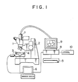
- Fig. 1 schematically illustrates an automatic structure analyzing/processing apparatus.
- numeral 1 denotes an optical microscope, to which an automatic focus adjusting mechanism 2 and a sample stage 4 controlled in X-axis and y-axis direction and having two set of gears and motors 3 having a positioning accuracy of ⁇ 1 ⁇ m are mounted.
- the apparatus of Fig. 1 denotes an optical microscope, to which an automatic focus adjusting mechanism 2 and a sample stage 4 controlled in X-axis and y-axis direction and having two set of gears and motors 3 having a positioning accuracy of ⁇ 1 ⁇ m are mounted.
- a computer 6 connected to the microscope 1 for moving the stage 4 by any amount of movement in the directions of the X and Y axes at any intervals of time to control a position of the stage 4 and storing information of a relative position of the stage 4 calculated back from the amount of movement into a memory 5, and a television camera 7 connected to the microscope 1 for taking a image of structure of a surface of material magnified by the optical microscope. Further, connected to the television camera 7 is an image processing device 8 which digitizes an electrical image signal and effects expansion or contraction of an image reproduced from the memory 5 or combination thereof to produce its image signal. The image processing device 8 is further connected to a display 9 and a printer 10, which displays and prints the image signal from the image processing device 8 as an image, respectively.
- the apparatus shown in Fig. 1 has been used to analyze structure of material used for a long time as a mechanical component.
- an area to be observed is a square area having 10mm x 10mm, which is fractionated vertically and horizontally into a plurality of small areas 11 having 0.2mm x 0.2mm. Then, the small areas 11 are marked with 1, 2, 3, ... starting from the upper left corner to the lower right corner in order and the relation of the small area and the marks is stored in the computer 6.
- An observation position at the upper left corner is determined with the optical microscope 1 and an image magnified to 300 times by the microscope of structure of the small area 11 marked by 1 is taken by the television camera 7 to supply it to the image processing device 8 as an electrical image signal, which is digitized to be stored in the memory 5 such as an optical disk together with the mark 1 of the small area 11. Then, the sample is moved by 0.2mm in the X-axis direction of Fig. 2 together with the sample stage 4 by the computer 6 so that the observation position of the optical microscope 1 is positioned to the small area 11 marked by 2 in Fig. 2. An image of structure of the small area 11 marked by 2 is stored in the memory 5 together with the mark 2 in the same manner as described above.
- the above operation is repeated 50 times to store the images of structure within 10 mm in the X-axis direction. Then, the sample is moved 0.2mm in the Y-axis direction and 9.8mm in the reverse direction to the X-axis direction together with the sample stage 4 by the computer 6 so that the observation position of the optical microscope 1 is positioned to the small area 11 marked by of Fig. 2. Images of structure of 50 small areas 11, which are magnified to 300 times by the microscope, are successively taken in the same manner as above and stored as image signals in the memory 5.
- the sample is moved 9.8mm by 0.2mm in the Y-axis direction while 50 images of structure are taken in the X-direction for each movement of 0.2mm in the Y-axis direction so that the recording operation is completed.
- a display screen of the display device 9 is fractionated into 50 x 50 small areas in the same manner as shown in Fig. 2 and the images of structure taken by the optical microscope and stored in the memory 5 are displayed on the small areas of the display 9 to combine all of the images into a signal image.
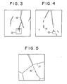
- Fig. 3 shows an image printed by the printer 10 of the combined image as described above. A broad distribution of cracked portions 12 in the component can be confirmed as shown in Fig. 3.
- Fig. 4 shows the enlarged image as obtained above. As can be seen from Fig. 4, it can be confirmed that there are many small cracks 14 at the end of the cracked portion 12 which could not be confirmed in the image shown in Fig. 3.
- the mark corresponding to the area 15 is detected by the computer 6 and only one image of the area 15 is displayed on the whole area of the display device 9 on an enlarged scale.
- Fig. 5 shows the enlarged image as obtained above. It can be confirmed that there exist many small cavities 16 on a crystal grain boundary 17 in the end of the small crack which could not be confirmed in the image shown in Figs. 3 and 4.
- the apparatus according to the present invention includes the automatic focus adjusting mechanism, structure having unevenness can be observed. Further, a small defect in a silicon wafer of a semiconductor or an optical disk, which can not be detected by a structure analyzer having a low magnification, can be inspected in a broad area and a position thereof can be displayed so that the apparatus of the present invention can be applied as a defect detector.
Landscapes
- Chemical & Material Sciences (AREA)
- Physics & Mathematics (AREA)
- Analytical Chemistry (AREA)
- General Physics & Mathematics (AREA)
- Biochemistry (AREA)
- Pathology (AREA)
- Signal Processing (AREA)
- Dispersion Chemistry (AREA)
- Health & Medical Sciences (AREA)
- Life Sciences & Earth Sciences (AREA)
- Optics & Photonics (AREA)
- General Health & Medical Sciences (AREA)
- Immunology (AREA)
- Engineering & Computer Science (AREA)
- Investigating Materials By The Use Of Optical Means Adapted For Particular Applications (AREA)
- Length Measuring Devices By Optical Means (AREA)
- Image Processing (AREA)
- Image Analysis (AREA)
- Investigating Or Analysing Materials By Optical Means (AREA)
- Microscoopes, Condenser (AREA)
- Sampling And Sample Adjustment (AREA)
- Analysing Materials By The Use Of Radiation (AREA)
Applications Claiming Priority (2)
| Application Number | Priority Date | Filing Date | Title |
|---|---|---|---|
| JP196287/88 | 1988-08-05 | ||
| JP63196287A JPH0245734A (ja) | 1988-08-05 | 1988-08-05 | 自動組織解析処理装置 |
Publications (2)
| Publication Number | Publication Date |
|---|---|
| EP0353504A2 true EP0353504A2 (de) | 1990-02-07 |
| EP0353504A3 EP0353504A3 (de) | 1991-04-03 |
Family
ID=16355292
Family Applications (1)
| Application Number | Title | Priority Date | Filing Date |
|---|---|---|---|
| EP19890112714 Withdrawn EP0353504A3 (de) | 1988-08-05 | 1989-07-12 | Automatische Vorrichtung zur Analyse/Behandlung einer Struktur |
Country Status (4)
| Country | Link |
|---|---|
| US (1) | US5038035A (de) |
| EP (1) | EP0353504A3 (de) |
| JP (1) | JPH0245734A (de) |
| KR (1) | KR910006221B1 (de) |
Cited By (4)
| Publication number | Priority date | Publication date | Assignee | Title |
|---|---|---|---|---|
| EP0557648A1 (de) * | 1992-02-21 | 1993-09-01 | Centro De Investigacion Y Desarrollo Condumex, S.A. De C.V. | Metallographisches Mikroskop zur Untersuchung von Zugdüsen für Leiter |
| EP0731371A1 (de) * | 1995-03-06 | 1996-09-11 | Perkin-Elmer Limited | Kontrolle eines Mikroskopprobenträgers |
| EP0819963A1 (de) * | 1996-07-16 | 1998-01-21 | Perkin-Elmer Limited | Kontrolle eines Infrarotmikroskops |
| WO1999049348A1 (de) * | 1998-03-23 | 1999-09-30 | Leica Microsystems Wetzlar Gmbh | Verfahren zur video-mikroskopie |
Families Citing this family (16)
| Publication number | Priority date | Publication date | Assignee | Title |
|---|---|---|---|---|
| JP2925647B2 (ja) * | 1990-04-16 | 1999-07-28 | オリンパス光学工業株式会社 | 顕微鏡変倍装置 |
| US5367401A (en) * | 1990-11-23 | 1994-11-22 | Perceptive Scientific Instruments, Inc. | Microscope slide rotary stage |
| US5587833A (en) * | 1993-07-09 | 1996-12-24 | Compucyte Corporation | Computerized microscope specimen encoder |
| CA2166464C (en) * | 1993-07-09 | 2002-01-01 | Louis A. Kamentsky | Computerized microscope specimen encoder |
| US5583464A (en) * | 1994-05-13 | 1996-12-10 | Thinking Machines Corporation | Resistor circuit for integrated circuit chip using insulated field effect transistors |
| CA2164369C (en) * | 1995-12-04 | 2006-01-24 | Roman Baldur | Portable fired cartridge imaging apparatus |
| DE69841245D1 (de) * | 1997-03-03 | 2009-11-26 | Olympus America Inc | Verfahren und Vorrichtung zur Erzeugung eines virtuellen Objektträgers für ein Mikroskop |
| KR20010015630A (ko) * | 1997-09-30 | 2001-02-26 | 칼 하인쯔 호르닝어 | 결함있는 전자 장치 식별 시스템 |
| EP1008956A1 (de) * | 1998-12-08 | 2000-06-14 | Synoptics Limited | Automatisches Bildmontagesystem |
| JP2002148526A (ja) * | 2000-11-06 | 2002-05-22 | Nikon Corp | 顕微鏡装置 |
| EP1368782A4 (de) * | 2001-01-16 | 2008-08-27 | Applied Precision Llc | Koordinatenkalibration für scan-systeme |
| JP2004343222A (ja) * | 2003-05-13 | 2004-12-02 | Olympus Corp | 画像処理装置 |
| CN100371762C (zh) * | 2005-02-25 | 2008-02-27 | 宝钢集团上海梅山有限公司 | 一种数码金相显微图像放大倍率的标定方法 |
| JP5321145B2 (ja) * | 2009-03-04 | 2013-10-23 | 日本電気株式会社 | 画像診断支援装置、画像診断支援方法、画像診断支援プログラム、及びその記憶媒体 |
| CN103163714A (zh) * | 2011-12-09 | 2013-06-19 | 无锡华润上华科技有限公司 | 显微镜机台结构 |
| EP3538941B1 (de) | 2016-11-10 | 2025-04-23 | The Trustees of Columbia University in the City of New York | Schnelles hochauflösendes bildgebungsverfahren für grosse proben |
Family Cites Families (18)
| Publication number | Priority date | Publication date | Assignee | Title |
|---|---|---|---|---|
| JPS5851664B2 (ja) * | 1979-03-28 | 1983-11-17 | 株式会社日立製作所 | 試料像表示装置 |
| US4366380A (en) * | 1979-10-11 | 1982-12-28 | George Mirkin | Method and apparatus for structural analysis |
| US4612614A (en) * | 1980-09-12 | 1986-09-16 | International Remote Imaging Systems, Inc. | Method of analyzing particles in a fluid sample |
| DE8105611U1 (de) * | 1981-02-27 | 1981-11-19 | Fa. Carl Zeiss, 7920 Heidenheim | Auswertevorrichtung fuer elektronenoptische bilder |
| US4468560A (en) * | 1982-02-11 | 1984-08-28 | Hitachi, Ltd. | Electron microscope equipped with measuring facility |
| JPS58153144A (ja) * | 1982-03-09 | 1983-09-12 | Nippon Kokan Kk <Nkk> | 反射率が異なる複数の組織を有する塊状物質における組織構成比率測定装置 |
| GB2134744B (en) * | 1983-01-15 | 1987-04-23 | Cambridge Instr Ltd | Movable energy probe microscope |
| US4680469A (en) * | 1984-08-17 | 1987-07-14 | Hitachi, Ltd. | Focusing device for a television electron microscope |
| EP0184810B1 (de) * | 1984-12-10 | 1994-06-29 | Fuji Photo Film Co., Ltd. | Verfahren zur Feststellung eines Fokussierungsfehlers eines elektronen-mikroskopischen Bildes |
| US4672559A (en) * | 1984-12-26 | 1987-06-09 | E. I. Du Pont De Nemours And Company | Method for operating a microscopical mapping system |
| JPS61226638A (ja) * | 1985-03-30 | 1986-10-08 | Shimadzu Corp | 顕微鏡分光像形成装置 |
| JPS62130305A (ja) * | 1985-12-03 | 1987-06-12 | Mitsutoyo Mfg Corp | 画像処理式測定装置 |
| NL8600685A (nl) * | 1986-03-18 | 1987-10-16 | Philips Nv | Apparaat voor energie selectieve afbeelding. |
| US4788426A (en) * | 1986-06-11 | 1988-11-29 | Kuehnle Manfred R | Interactive image recording method and means |
| NL8602175A (nl) * | 1986-08-27 | 1988-03-16 | Philips Nv | Werkwijze voor bundelcentrering. |
| JP2702114B2 (ja) * | 1986-10-03 | 1998-01-21 | 株式会社日立製作所 | 電子顕微鏡 |
| US4872052A (en) * | 1986-12-03 | 1989-10-03 | View Engineering, Inc. | Semiconductor device inspection system |
| JPH06105605B2 (ja) * | 1987-09-11 | 1994-12-21 | 株式会社日立製作所 | 電子顕微鏡の像観察装置 |
-
1988
- 1988-08-05 JP JP63196287A patent/JPH0245734A/ja active Pending
-
1989
- 1989-07-06 US US07/376,664 patent/US5038035A/en not_active Expired - Fee Related
- 1989-07-12 EP EP19890112714 patent/EP0353504A3/de not_active Withdrawn
- 1989-08-04 KR KR1019890011160A patent/KR910006221B1/ko not_active Expired
Cited By (6)
| Publication number | Priority date | Publication date | Assignee | Title |
|---|---|---|---|---|
| EP0557648A1 (de) * | 1992-02-21 | 1993-09-01 | Centro De Investigacion Y Desarrollo Condumex, S.A. De C.V. | Metallographisches Mikroskop zur Untersuchung von Zugdüsen für Leiter |
| EP0731371A1 (de) * | 1995-03-06 | 1996-09-11 | Perkin-Elmer Limited | Kontrolle eines Mikroskopprobenträgers |
| US6006140A (en) * | 1995-03-06 | 1999-12-21 | Perkin-Elmer Ltd. | Infrared microscope stage control |
| EP0819963A1 (de) * | 1996-07-16 | 1998-01-21 | Perkin-Elmer Limited | Kontrolle eines Infrarotmikroskops |
| WO1999049348A1 (de) * | 1998-03-23 | 1999-09-30 | Leica Microsystems Wetzlar Gmbh | Verfahren zur video-mikroskopie |
| US6944326B1 (en) | 1998-03-23 | 2005-09-13 | Leica Microsystems Wetzlar Gmbh | Video microscopy method |
Also Published As
| Publication number | Publication date |
|---|---|
| JPH0245734A (ja) | 1990-02-15 |
| EP0353504A3 (de) | 1991-04-03 |
| US5038035A (en) | 1991-08-06 |
| KR900003621A (ko) | 1990-03-26 |
| KR910006221B1 (ko) | 1991-08-17 |
Similar Documents
| Publication | Publication Date | Title |
|---|---|---|
| EP0353504A2 (de) | Automatische Vorrichtung zur Analyse/Behandlung einer Struktur | |
| KR100969413B1 (ko) | 압흔 경도 시험 시스템 | |
| US5539656A (en) | Crack monitoring apparatus | |
| US5117110A (en) | Composite scanning tunnelling microscope with a positioning function | |
| US4727179A (en) | Method and apparatus for position control of plant parts in a highly radioactive cell for an atomic plant | |
| JPH0735645A (ja) | 液晶パネルの検査装置 | |
| US5822875A (en) | Scanning electron microscopic ruler and method | |
| JP2991483B2 (ja) | 顕微鏡イメージマッピング装置及び方法 | |
| JPH1195125A5 (de) | ||
| JPS6249481A (ja) | イメ−ジのデイジタル化方法および装置 | |
| GB2138240A (en) | Method to superimpose a reference standard onto the image of a microscope | |
| JPS6126715B2 (de) | ||
| JPH07225121A (ja) | 外観検査装置 | |
| JPH01321151A (ja) | Ccd画素を用いた工具測定調整装置 | |
| JPH09280828A (ja) | 原子力燃料集合体の外観検査装置 | |
| JP2939323B2 (ja) | 非金属介在物検査方法並びに非金属介在物検査装置 | |
| EP1422648B1 (de) | System und Verfahren zur Inspektion von Probenbildern | |
| JPH07333517A (ja) | ステ−ジ座標記録機構を有する顕微鏡システム | |
| JPH0429363Y2 (de) | ||
| JP2968915B2 (ja) | プローブ顕微鏡装置の位置決め方法 | |
| JP4830775B2 (ja) | X線検査装置 | |
| JPH06288927A (ja) | 画像処理検査方法 | |
| JPH08327909A (ja) | 検鏡支援装置 | |
| US4574306A (en) | Apparatus and method for automatically measuring the shoe-length of a video disc stylus | |
| JP2000105167A (ja) | 画質検査装置のアドレス・キャリブレーション方法 |
Legal Events
| Date | Code | Title | Description |
|---|---|---|---|
| PUAI | Public reference made under article 153(3) epc to a published international application that has entered the european phase |
Free format text: ORIGINAL CODE: 0009012 |
|
| AK | Designated contracting states |
Kind code of ref document: A2 Designated state(s): DE FR GB |
|
| PUAL | Search report despatched |
Free format text: ORIGINAL CODE: 0009013 |
|
| AK | Designated contracting states |
Kind code of ref document: A3 Designated state(s): DE FR GB |
|
| 17P | Request for examination filed |
Effective date: 19910517 |
|
| 17Q | First examination report despatched |
Effective date: 19921201 |
|
| STAA | Information on the status of an ep patent application or granted ep patent |
Free format text: STATUS: THE APPLICATION IS DEEMED TO BE WITHDRAWN |
|
| 18D | Application deemed to be withdrawn |
Effective date: 19930414 |