EP0353885A2 - Anisotropie perpendiculaire dans des dispositifs en films minces - Google Patents
Anisotropie perpendiculaire dans des dispositifs en films minces Download PDFInfo
- Publication number
- EP0353885A2 EP0353885A2 EP89307057A EP89307057A EP0353885A2 EP 0353885 A2 EP0353885 A2 EP 0353885A2 EP 89307057 A EP89307057 A EP 89307057A EP 89307057 A EP89307057 A EP 89307057A EP 0353885 A2 EP0353885 A2 EP 0353885A2
- Authority
- EP
- European Patent Office
- Prior art keywords
- layer
- magnetic
- pole
- domains
- flux
- Prior art date
- Legal status (The legal status is an assumption and is not a legal conclusion. Google has not performed a legal analysis and makes no representation as to the accuracy of the status listed.)
- Granted
Links
- 239000010409 thin film Substances 0.000 title claims description 22
- 230000004907 flux Effects 0.000 claims abstract description 73
- 239000000758 substrate Substances 0.000 claims abstract description 31
- 230000007480 spreading Effects 0.000 claims abstract description 7
- 238000003892 spreading Methods 0.000 claims abstract description 7
- 238000000034 method Methods 0.000 claims description 58
- 239000010408 film Substances 0.000 claims description 16
- 238000000151 deposition Methods 0.000 claims description 14
- 230000005381 magnetic domain Effects 0.000 claims description 12
- 230000005415 magnetization Effects 0.000 claims description 5
- 229910000531 Co alloy Inorganic materials 0.000 claims description 4
- 229910000640 Fe alloy Inorganic materials 0.000 claims description 4
- 229910000990 Ni alloy Inorganic materials 0.000 claims description 4
- 239000002223 garnet Substances 0.000 claims description 4
- 238000007747 plating Methods 0.000 claims description 4
- 238000001771 vacuum deposition Methods 0.000 claims description 4
- 229910000859 α-Fe Inorganic materials 0.000 claims description 4
- 238000000137 annealing Methods 0.000 claims description 3
- 230000001939 inductive effect Effects 0.000 claims description 3
- 230000033001 locomotion Effects 0.000 description 6
- 230000007547 defect Effects 0.000 description 3
- 230000008021 deposition Effects 0.000 description 3
- 239000000463 material Substances 0.000 description 3
- 230000008569 process Effects 0.000 description 3
- 230000005330 Barkhausen effect Effects 0.000 description 2
- XEEYBQQBJWHFJM-UHFFFAOYSA-N Iron Chemical compound [Fe] XEEYBQQBJWHFJM-UHFFFAOYSA-N 0.000 description 2
- 230000008901 benefit Effects 0.000 description 2
- 230000015572 biosynthetic process Effects 0.000 description 2
- 239000000919 ceramic Substances 0.000 description 2
- 239000013078 crystal Substances 0.000 description 2
- 238000004519 manufacturing process Methods 0.000 description 2
- 230000003068 static effect Effects 0.000 description 2
- 229910001030 Iron–nickel alloy Inorganic materials 0.000 description 1
- 229910018104 Ni-P Inorganic materials 0.000 description 1
- 229910018536 Ni—P Inorganic materials 0.000 description 1
- PNEYBMLMFCGWSK-UHFFFAOYSA-N aluminium oxide Inorganic materials [O-2].[O-2].[O-2].[Al+3].[Al+3] PNEYBMLMFCGWSK-UHFFFAOYSA-N 0.000 description 1
- 230000005540 biological transmission Effects 0.000 description 1
- 230000008859 change Effects 0.000 description 1
- 239000010941 cobalt Substances 0.000 description 1
- GUTLYIVDDKVIGB-UHFFFAOYSA-N cobalt atom Chemical compound [Co] GUTLYIVDDKVIGB-UHFFFAOYSA-N 0.000 description 1
- 229910052802 copper Inorganic materials 0.000 description 1
- 229910052593 corundum Inorganic materials 0.000 description 1
- 238000000469 dry deposition Methods 0.000 description 1
- 238000005516 engineering process Methods 0.000 description 1
- 229910052737 gold Inorganic materials 0.000 description 1
- 239000011810 insulating material Substances 0.000 description 1
- 230000007246 mechanism Effects 0.000 description 1
- 239000002184 metal Substances 0.000 description 1
- 229910052751 metal Inorganic materials 0.000 description 1
- 230000003094 perturbing effect Effects 0.000 description 1
- 230000000644 propagated effect Effects 0.000 description 1
- 230000001902 propagating effect Effects 0.000 description 1
- 230000035945 sensitivity Effects 0.000 description 1
- 238000004544 sputter deposition Methods 0.000 description 1
- 238000000992 sputter etching Methods 0.000 description 1
- 229910001845 yogo sapphire Inorganic materials 0.000 description 1
- 229910052727 yttrium Inorganic materials 0.000 description 1
Images

Classifications
-
- G—PHYSICS
- G11—INFORMATION STORAGE
- G11B—INFORMATION STORAGE BASED ON RELATIVE MOVEMENT BETWEEN RECORD CARRIER AND TRANSDUCER
- G11B5/00—Recording by magnetisation or demagnetisation of a record carrier; Reproducing by magnetic means; Record carriers therefor
- G11B5/127—Structure or manufacture of heads, e.g. inductive
- G11B5/31—Structure or manufacture of heads, e.g. inductive using thin films
- G11B5/3109—Details
- G11B5/3113—Details for improving the magnetic domain structure or avoiding the formation or displacement of undesirable magnetic domains
-
- G—PHYSICS
- G11—INFORMATION STORAGE
- G11B—INFORMATION STORAGE BASED ON RELATIVE MOVEMENT BETWEEN RECORD CARRIER AND TRANSDUCER
- G11B5/00—Recording by magnetisation or demagnetisation of a record carrier; Reproducing by magnetic means; Record carriers therefor
- G11B5/127—Structure or manufacture of heads, e.g. inductive
- G11B5/31—Structure or manufacture of heads, e.g. inductive using thin films
- G11B5/3109—Details
- G11B5/3116—Shaping of layers, poles or gaps for improving the form of the electrical signal transduced, e.g. for shielding, contour effect, equalizing, side flux fringing, cross talk reduction between heads or between heads and information tracks
-
- G—PHYSICS
- G11—INFORMATION STORAGE
- G11B—INFORMATION STORAGE BASED ON RELATIVE MOVEMENT BETWEEN RECORD CARRIER AND TRANSDUCER
- G11B5/00—Recording by magnetisation or demagnetisation of a record carrier; Reproducing by magnetic means; Record carriers therefor
- G11B5/127—Structure or manufacture of heads, e.g. inductive
- G11B5/33—Structure or manufacture of flux-sensitive heads, i.e. for reproduction only; Combination of such heads with means for recording or erasing only
- G11B5/332—Structure or manufacture of flux-sensitive heads, i.e. for reproduction only; Combination of such heads with means for recording or erasing only using thin films
-
- H—ELECTRICITY
- H01—ELECTRIC ELEMENTS
- H01F—MAGNETS; INDUCTANCES; TRANSFORMERS; SELECTION OF MATERIALS FOR THEIR MAGNETIC PROPERTIES
- H01F41/00—Apparatus or processes specially adapted for manufacturing or assembling magnets, inductances or transformers; Apparatus or processes specially adapted for manufacturing materials characterised by their magnetic properties
- H01F41/14—Apparatus or processes specially adapted for manufacturing or assembling magnets, inductances or transformers; Apparatus or processes specially adapted for manufacturing materials characterised by their magnetic properties for applying magnetic films to substrates
-
- Y—GENERAL TAGGING OF NEW TECHNOLOGICAL DEVELOPMENTS; GENERAL TAGGING OF CROSS-SECTIONAL TECHNOLOGIES SPANNING OVER SEVERAL SECTIONS OF THE IPC; TECHNICAL SUBJECTS COVERED BY FORMER USPC CROSS-REFERENCE ART COLLECTIONS [XRACs] AND DIGESTS
- Y10—TECHNICAL SUBJECTS COVERED BY FORMER USPC
- Y10T—TECHNICAL SUBJECTS COVERED BY FORMER US CLASSIFICATION
- Y10T428/00—Stock material or miscellaneous articles
- Y10T428/11—Magnetic recording head
- Y10T428/1171—Magnetic recording head with defined laminate structural detail
- Y10T428/1186—Magnetic recording head with defined laminate structural detail with head pole component
Definitions
- the present invention relates to thin film magnetic devices having perpendicular anisotropy.
- Magnetic devices such as thin film recording heads, whether read, read/write, or write, are designed to have particular magnetic orientations, or domains, within the active regions of the device material.
- the static state of each of these domains can be configured as desired, by control of the manufacturing process. Performance is critically linked to domain formation, and, therefore, control can be exerted over device performance by controlling domain formation.
- Conduction of flux is achieved by two mechanisms: domain wall motion and domain rotation.
- Domain wall motion results in flux being transmitted through a thin film head along the walls of a domain, or domains, the flux spreading out along the domain walls as the flux seeks to return to equilibrium.
- domain wall motion facilitates conduction of flux at low frequencies, it is a poor vehicle for conduction of flux at high frequencies.
- defects in the material in a magnetic head can be the source of Barkhausen noise during conduction of flux by wall motion as the flux is perturbed by these defects. Such noise can result in erroneous readings of recorded data.
- Conduction of flux by domain rotation may be achieved by configuring a series of neighboring domains axially aligned along parallel axes, where flux impinged upon the first domain at a given angle will cause the magnetization of that domain to rotate from its static orientation by that angle radially into and impinging upon the neighboring domain.
- Such rotation can be transmitted in a like manner along an axis of flux transmission by each neighboring domain of the series.
- flux can be conducted in the pole and through the yoke of a thin film head in a series of domain rotations.
- the yoke enables conduction of flux through a transducer which produces electrical signals proportional to flux levels or the rate of change of flux. Where the yoke reluctance is high, a significant amount of flux will bypass the transducer, and thus the device output will be reduced.
- Certain prior art devices such as thin film heads, are commonly produced having an anisotropy (at rest domain orientation) parallel to the plane of the substrate and transverse to the signal flux axis.
- anisotropy at rest domain orientation
- the region of transverse magnetization which can transmit flux by rotation, shrinks toward zero. This results from edge domains (longitudinally oriented flux closure regions) dominating the flux path and preventing conduction by rotation.
- the head will therefore exhibit high reluctance at high frequencies.
- a further artifact in conventional recording heads having the above orientation is that even where flux is conducted by rotation, the flux cannot substantially spread as it travels longitudinally from the pole tip through the yoke, since domain rotation can conduct flux efficiently only in the in-plane longitudinal direction in such devices, the other available direction being out-of plane and of high reluctance.
- One aspect of the present invention relates to enabling rotational flux conduction through magnetic film devices by creating a magnetic film layer with anisotropy perpendicular to the plane of the film layer, the film layer deposited in sufficient thickness so that there is a rest state rotational conduction path in the plane of the film layer.
- One feature of the present invention enables forming perpendicularly oriented central domains in a magnetic device so that the path for conduction of signal flux by rotation remains open even for very narrow signal flux paths.
- Another feature of the invention is to orient at rest domain states of a magnetic device pole (or poles) perpendicular to two desired in-plane rotational flux travel directions.
- Another feature of the invention is to orient edge domains in this type of magnetic pole into a plane where their relative widths do not impact substantially on rotational flux flow through the pole for narrow track heads.
- Another aspect of the invention is to provide for flux spreading in a magnetic device having perpendicular anisotropy.
- a preferred embodiment of the present invention includes at least one layer of a magnetic device, formed on a substrate, having a preferred at rest pole domain orientation perpendicular to the substrate plane.
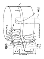
- Fig. 1 is a perspective view from a magnetic recording medium (not shown) looking into the pole tips 16, 18 of a conventional two pole magnetic recording head 10. Pole tips 16, 18, of respective poles 12, 14, are shown exposed to the medium, each pole having a thickness t at its tip.
- each pole of such conventional device typically has a center region 21 defined by a plurality of transverse domains 20, all aligned along common parallel axes perpendicular to the axis of signal flux flow. The rest state magnetic orientation of each domain 20 is as indicated by the arrow within each such domain, and lies in the X-axis.
- This transverse orientation will facilitate rotational flux conduction, where flux will be propagated serially through adjacent domains 20 as it flows toward the rear 17 of yoke section 15 along the longitudinal Y-axis.
- the Z-axis is out of plane and is therefore a high reluctance path.
- An inductive transducer 13 is shown schematically in the yoke midsection where it will be capable of sensing or inducing signal flux flow.
- edge domains 22 On either side of central region A, in the transverse direction, are edge domains 22. Each of these edge domains has a width W x . They are oriented longitudinally as indicated by the arrow within each such domain. The domains 22 do not facilitate conduction by rotation, but rather act as closure domains in conjunction with adjacent domains 20 and also act to reduce rotational conduction efficiency.
- Poles 12 and 14 are separated by a gap layer g, which in Fig. 1 is shown disproportionately large. It will be appreciated by those skilled in the art that gap g ordinarily would take the form of an insulating material such as Al2O3, laid down as part of a multistep growth process of forming a plurality of heads 10 upon a substrate. A typical gap width range might be 0.2 to 1.0 microns.
- a track of oriented magnetization will be created having a width which is defined by the operational width W t of head 10. Furthermore, as shown in fig. 1, track width W t will be understood as the sum of undesired edge domain 22 width 2W x (i.e., W x +W x ) and desired central region width W r .
- the signal from the track will be conducted from tip to yoke only in the central transversely oriented region W r of head 10.
- track width is driven smaller.
- the width W r of central region 21 reduces by an even greater proportion toward zero.
- rotational conduction is driven toward zero as track width narrows in conventional heads.
- a thin film magnetic device such as a recording head 30, has two poles 32 and 34.
- the poles are formed, one on top of the other, parallel to the substrate deposition plane in the direction of film thickness axis T, separated by gap layer g.
- Pole 32 is configured having a plurality of central domains 36.
- Pole 34 is similarly configured. These domains are anisotropically oriented perpendicular to the substrate deposition plane.
- the desired central domain width W r becomes equal to track width W t .
- width W t can be reduced substantially without concern for the perturbing effect of the 2W x edge domain factor.
- edge domains are inherent in thin film heads, and edge domains 38 now will be seen located on the far interior or exterior edges of poles 32, 34.
- these edge domains will have been relegated by this configuration to the head thickness dimension (which is not critical to maintaining the rotational beam provided that the poles are of sufficient thickness) rather than width (which is critical).
- the head may be plated to sufficient thickness T, where the edge domains 38 at the far horizontal surfaces of the poles are small relative to central domains 36, and thus do not dominate flux conduction.
- domains 36 will have varying widths, spreading out from the narrow tip toward the center of the yoke. Hence, the width of domain 36 o at the pole tip will be less than the width W n of domain 36 n near the yoke midsection. Depending upon yoke configuration, domains 36 may begin to reduce in width heading toward the very back of the yoke. This narrowing will not prevent conduction by rotation.
- transducer in this device will be associated with the yoke section, and is shown schematically as inductor 13. However, various transducer configurations would be operable within practice of the present invention.
- Premagnetization of domains 36 is in the perpendicular (Z) direction (thickness), which leaves two horizontal (X, Y) directions (transverse and longitudinal) available for conduction by rotation in the planes of the poles.
- Z perpendicular
- X, Y horizontal
- transverse and longitudinal available for conduction by rotation in the planes of the poles.
- signal flux from the medium interacts with the head pole tips 42, 44. Then, sequentially, each domain 36 reacts by rotating by an angle phi, thus propagating the signal flux down to the yoke of the device. This avoids the defects of conduction by wall motion, by removing the perturbation of edge domains, suppressing unwanted Barkhausen noise, and also enables flux spreading.
- the film thicker than normal, perhaps about or greater than three microns.
- the gap g at the pole tips may be of conventional thickness.
- the ideal track width at which it pays to utilize the present invention is defined at the point where the width W t is almost equal to 2W x (i.e., W r and the rotational signal flux path are approaching zero).
- the perpendicularly oriented layer (or layers) can be deposited on a wafer substrate by placing the wafer in a perpendicularly oriented magnetic field during deposition.
- the perpendicularly oriented magnetic field can be supplied by coils or by the magnetron target magnets of a sputtering machine, for example.
- orientation can be accomplished by growing the film with a crystal orientation that places a crystallographically oriented axis in the perpendicularly oriented direction.
- Another approach includes the steps of depositing a pole with negative magnetostriction and tensile stress such that magnetic anisotropy is induced in the perpendicular direction.
- a gap layer (non magnetic) can be deposited.
- a ceramic For dry deposition, it is convenient to use a ceramic.
- the yoke and the transducer may be formed by means of a masked ion milling process.
- each pole layer is deposited through a plating mask in a bias field to establish appropriate magnetic domain orientation.
- the non-magnetic layer can be plated if it is a metal, for example Ni-P, Au, Cu, etc. If a ceramic is used for the buffer layer, then this must be sputtered after the mask has been removed.
- the structure is now ready to receive the next magnetic pole, whereupon a seed layer and mask will be laid down, and the pole will be plated thereon.
- a problem with the technology described above resides in that any exposure to very high temperatures (for example, greater than 200°C for greater than half an hour for NiFe or NiFeCo poles) will degrade the induced anisotropy obtained by depositing in a field. This sensitivity can be overcome by annealing at high temperatures in a strong perpendicular field.
- Pole materials which may be used in the above processes including alloys of nickel, iron and cobalt, and magnetic garnet and magnetic ferrite crystals, to name a few alternatives
Landscapes
- Engineering & Computer Science (AREA)
- Manufacturing & Machinery (AREA)
- Power Engineering (AREA)
- Magnetic Heads (AREA)
- Physical Deposition Of Substances That Are Components Of Semiconductor Devices (AREA)
- Laminated Bodies (AREA)
- Crystals, And After-Treatments Of Crystals (AREA)
- Thin Magnetic Films (AREA)
Applications Claiming Priority (2)
| Application Number | Priority Date | Filing Date | Title |
|---|---|---|---|
| US22781388A | 1988-08-03 | 1988-08-03 | |
| US227813 | 1988-08-03 |
Publications (3)
| Publication Number | Publication Date |
|---|---|
| EP0353885A2 true EP0353885A2 (fr) | 1990-02-07 |
| EP0353885A3 EP0353885A3 (fr) | 1993-06-30 |
| EP0353885B1 EP0353885B1 (fr) | 1995-08-30 |
Family
ID=22854573
Family Applications (1)
| Application Number | Title | Priority Date | Filing Date |
|---|---|---|---|
| EP89307057A Expired - Lifetime EP0353885B1 (fr) | 1988-08-03 | 1989-07-12 | Anisotropie perpendiculaire dans des dispositifs en films minces |
Country Status (6)
| Country | Link |
|---|---|
| US (1) | US5384680A (fr) |
| EP (1) | EP0353885B1 (fr) |
| JP (1) | JPH0289207A (fr) |
| AT (1) | ATE127264T1 (fr) |
| CA (1) | CA1334447C (fr) |
| DE (1) | DE68924017T2 (fr) |
Cited By (3)
| Publication number | Priority date | Publication date | Assignee | Title |
|---|---|---|---|---|
| EP0401983B1 (fr) * | 1989-06-02 | 1995-11-15 | Quantum Corporation | Dispositif de film mince avec conduction rotative de flux magnétique |
| EP0353911B1 (fr) * | 1988-08-03 | 1996-01-31 | Quantum Corporation | Dispositifs en films minces magnétiques pour propagation de flux |
| AU2002319964B2 (en) * | 2002-07-30 | 2009-10-29 | Nestec S.A. | A system for dispensing a liquid substance |
Families Citing this family (6)
| Publication number | Priority date | Publication date | Assignee | Title |
|---|---|---|---|---|
| US5170303A (en) * | 1990-04-30 | 1992-12-08 | Seagate Technology Inc. | Inductive thin film head having improved readback characteristics |
| JPH0773412A (ja) * | 1993-06-24 | 1995-03-17 | Sanyo Electric Co Ltd | 薄膜磁気ヘッド |
| JP2001256608A (ja) * | 2000-03-14 | 2001-09-21 | Toshiba Corp | 磁気ヘッド及び磁気記憶再生装置 |
| JP4061139B2 (ja) * | 2002-07-04 | 2008-03-12 | 新科實業有限公司 | 垂直磁気記録ヘッドおよびその製造方法 |
| US7113366B1 (en) * | 2002-11-07 | 2006-09-26 | Western Digital (Fremont), Inc. | Double-nosed inductive transducer with reduced off-track writing |
| US8817417B2 (en) | 2012-12-26 | 2014-08-26 | Tdk Corporation | Perpendicular magnetic write head and magnetic recording device |
Family Cites Families (38)
| Publication number | Priority date | Publication date | Assignee | Title |
|---|---|---|---|---|
| US3880602A (en) * | 1967-07-28 | 1975-04-29 | Centre Nat Rech Scient | Thin layer magnetic structures for binary information stores |
| US3961299A (en) * | 1969-10-28 | 1976-06-01 | Commissariat A L'energie Atomique | Magnetic circuit having low reluctance |
| US3967368A (en) * | 1972-10-11 | 1976-07-06 | International Business Machines Corporation | Method for manufacturing and using an internally biased magnetoresistive magnetic transducer |
| FR2248566B1 (fr) * | 1973-10-23 | 1976-11-19 | Cii | |
| JPS52131711A (en) * | 1976-04-28 | 1977-11-04 | Kokusai Denshin Denwa Co Ltd | Thin film magnetic head |
| US4103315A (en) * | 1977-06-24 | 1978-07-25 | International Business Machines Corporation | Antiferromagnetic-ferromagnetic exchange bias films |
| JPS5459915A (en) * | 1977-10-20 | 1979-05-15 | Sony Corp | Method and apparatus for reading of magnetic recording signal |
| US4242710A (en) * | 1979-01-29 | 1980-12-30 | International Business Machines Corporation | Thin film head having negative magnetostriction |
| US4374403A (en) * | 1979-06-27 | 1983-02-15 | Matsushita Electric Industrial Co., Ltd. | Magnetic recording and reproducing system |
| US4413296A (en) * | 1979-07-16 | 1983-11-01 | Eastman Kodak Company | Thin film magnetoresistive head |
| US4295173A (en) * | 1979-10-18 | 1981-10-13 | International Business Machines Corporation | Thin film inductive transducer |
| JPS56163517A (en) * | 1980-05-19 | 1981-12-16 | Fujitsu Ltd | Vertical magnetization recording head |
| US4356523A (en) * | 1980-06-09 | 1982-10-26 | Ampex Corporation | Narrow track magnetoresistive transducer assembly |
| JPS57141013A (en) * | 1981-02-25 | 1982-09-01 | Canon Electronics Inc | Thin film magnetic sensor |
| JPS57164416A (en) * | 1981-03-31 | 1982-10-09 | Fujitsu Ltd | Magnetic head |
| NL8200481A (nl) * | 1982-02-09 | 1983-09-01 | Philips Nv | Magneetkop. |
| DE3374622D1 (en) * | 1982-04-14 | 1987-12-23 | Matsushita Electric Industrial Co Ltd | A playback head for perpendicular magnetic recordings |
| US4564877A (en) * | 1982-04-28 | 1986-01-14 | Tdk Corporation | Magnetic recording/reproducing system with wide-gapped transducer and method for using same |
| NL8204897A (nl) * | 1982-12-20 | 1984-07-16 | Philips Nv | Magneetkop met een kern van mn-zn-co-ferroferriet. |
| JPS59121611A (ja) * | 1982-12-28 | 1984-07-13 | Fujitsu Ltd | 磁気ヘツド |
| US4566050A (en) * | 1982-12-30 | 1986-01-21 | International Business Machines Corp. (Ibm) | Skew insensitive magnetic read head |
| US4535375A (en) * | 1983-01-14 | 1985-08-13 | Magnetic Peripherals, Inc. | Magnetoresistive head |
| DE3346876A1 (de) * | 1983-12-23 | 1985-07-11 | Siemens AG, 1000 Berlin und 8000 München | Kombinierter schreib- und lese-magnetkopf zur senkrechten magnetisierung eines entsprechenden aufzeichnungsmediums |
| US4626946A (en) * | 1984-02-28 | 1986-12-02 | International Business Machines Corporation | Twin track vertical read-write head structure |
| DE3527468A1 (de) * | 1984-08-01 | 1986-02-06 | Matsushita Electric Industrial Co., Ltd., Kadoma, Osaka | Magnetkopf fuer quermagnetische aufzeichnung und wiedergabe |
| US4656546A (en) * | 1985-01-22 | 1987-04-07 | Digital Equipment Corporation | Vertical magnetic recording arrangement |
| JPS61192011A (ja) * | 1985-02-20 | 1986-08-26 | Hitachi Ltd | 薄膜磁気ヘツド |
| US4668913A (en) * | 1985-03-14 | 1987-05-26 | International Business Machines Corporation | Constant flux magneto resistive magnetic reluctance sensing apparatus |
| JPH069083B2 (ja) * | 1985-04-04 | 1994-02-02 | 日本電気株式会社 | 垂直磁気ヘッド |
| US4663685A (en) * | 1985-08-15 | 1987-05-05 | International Business Machines | Magnetoresistive read transducer having patterned longitudinal bias |
| US4649447A (en) * | 1985-08-15 | 1987-03-10 | International Business Machines | Combed MR sensor |
| US4698711A (en) * | 1985-10-02 | 1987-10-06 | International Business Machines Corporation | Simplified, shielded twin-track read/write head structure |
| US4695351A (en) * | 1986-07-10 | 1987-09-22 | Digital Equipment Corporation | Method for producing magnetic heads |
| US4803580A (en) * | 1987-02-17 | 1989-02-07 | Magnetic Peripherals Inc. | Double-gap magnetoresistive head having an elongated central write/shield pole completely shielding the magnetoresistive sensor strip in the read gap |
| US4891725A (en) * | 1987-02-17 | 1990-01-02 | Magnetic Peripherals Inc. | Magnetoresistive sensor having antiferromagnetic exchange-biased ends |
| US4825318A (en) * | 1987-06-05 | 1989-04-25 | Carnegie-Mellon University | Compound read/write element for rigid magnetic disk files |
| US4816947A (en) * | 1987-11-12 | 1989-03-28 | International Business Machines | Single track vertical and horizontal recording read/write head design |
| US4912584A (en) * | 1988-03-09 | 1990-03-27 | Digital Equipment Corporation | Method for fabricating magnetic recording poles |
-
1989
- 1989-07-04 CA CA000604710A patent/CA1334447C/fr not_active Expired - Fee Related
- 1989-07-12 EP EP89307057A patent/EP0353885B1/fr not_active Expired - Lifetime
- 1989-07-12 AT AT89307057T patent/ATE127264T1/de not_active IP Right Cessation
- 1989-07-12 DE DE68924017T patent/DE68924017T2/de not_active Expired - Fee Related
- 1989-08-01 JP JP1200125A patent/JPH0289207A/ja active Pending
-
1993
- 1993-02-16 US US08/017,998 patent/US5384680A/en not_active Expired - Fee Related
Cited By (3)
| Publication number | Priority date | Publication date | Assignee | Title |
|---|---|---|---|---|
| EP0353911B1 (fr) * | 1988-08-03 | 1996-01-31 | Quantum Corporation | Dispositifs en films minces magnétiques pour propagation de flux |
| EP0401983B1 (fr) * | 1989-06-02 | 1995-11-15 | Quantum Corporation | Dispositif de film mince avec conduction rotative de flux magnétique |
| AU2002319964B2 (en) * | 2002-07-30 | 2009-10-29 | Nestec S.A. | A system for dispensing a liquid substance |
Also Published As
| Publication number | Publication date |
|---|---|
| JPH0289207A (ja) | 1990-03-29 |
| DE68924017T2 (de) | 1996-01-25 |
| EP0353885B1 (fr) | 1995-08-30 |
| CA1334447C (fr) | 1995-02-14 |
| EP0353885A3 (fr) | 1993-06-30 |
| DE68924017D1 (de) | 1995-10-05 |
| ATE127264T1 (de) | 1995-09-15 |
| US5384680A (en) | 1995-01-24 |
Similar Documents
| Publication | Publication Date | Title |
|---|---|---|
| EP0463753B1 (fr) | Configuration de pÔle magnétique pour tête d'enregistrement de film mince à haute densité | |
| US6223420B1 (en) | Method of making a read head with high resistance soft magnetic flux guide layer for enhancing read sensor efficiency | |
| US4896235A (en) | Magnetic transducer head utilizing magnetoresistance effect | |
| US5085935A (en) | Flux spreading thin film magnetic devices | |
| JPS59210630A (ja) | 磁気薄膜構造体の製造方法 | |
| JPH03254412A (ja) | 磁性薄膜構造体及びその製造方法 | |
| EP0353911B1 (fr) | Dispositifs en films minces magnétiques pour propagation de flux | |
| EP0353885B1 (fr) | Anisotropie perpendiculaire dans des dispositifs en films minces | |
| JPH0687287B2 (ja) | 複数個の磁気抵抗読取り変換器を一括製造する方法 | |
| US6376108B1 (en) | Magnetic material and magnetic head using the same and magnetic storage device having thereof | |
| JP3394266B2 (ja) | 磁気書込/読取ヘッドの製造方法 | |
| EP0480324B1 (fr) | Tête magnétique en films minces | |
| US5331496A (en) | Thin-film magnetic transducer with a multitude of magnetic flux interactions | |
| US4394699A (en) | Thin-film magnetic head | |
| JP3130407B2 (ja) | 磁性膜の製法および薄膜磁気ヘッド | |
| JPS61179509A (ja) | 磁性材料 | |
| JPS6032885B2 (ja) | 薄膜磁気ヘッド | |
| EP0694911B1 (fr) | Tête à effet de magnétorésistance pour lecture et écriture | |
| JP2614203B2 (ja) | 磁気抵抗効果ヘツド | |
| JPS60124014A (ja) | 垂直磁気ヘッド装置およびその製造方法 | |
| JPH01196711A (ja) | 薄膜磁気ヘッド | |
| JPS6233413A (ja) | 軟磁性薄膜コアの製造方法 | |
| JPH0289206A (ja) | 薄膜磁気ヘッド | |
| JPH07107731B2 (ja) | ヨ−ク型薄膜磁気ヘツド | |
| JPH0276111A (ja) | 薄膜磁気ヘッド |
Legal Events
| Date | Code | Title | Description |
|---|---|---|---|
| PUAI | Public reference made under article 153(3) epc to a published international application that has entered the european phase |
Free format text: ORIGINAL CODE: 0009012 |
|
| 17P | Request for examination filed |
Effective date: 19890721 |
|
| AK | Designated contracting states |
Kind code of ref document: A2 Designated state(s): AT BE CH DE ES FR GB GR IT LI LU NL SE |
|
| PUAL | Search report despatched |
Free format text: ORIGINAL CODE: 0009013 |
|
| AK | Designated contracting states |
Kind code of ref document: A3 Designated state(s): AT BE CH DE ES FR GB GR IT LI LU NL SE |
|
| 17Q | First examination report despatched |
Effective date: 19931022 |
|
| RAP1 | Party data changed (applicant data changed or rights of an application transferred) |
Owner name: QUANTUM CORPORATION |
|
| GRAA | (expected) grant |
Free format text: ORIGINAL CODE: 0009210 |
|
| AK | Designated contracting states |
Kind code of ref document: B1 Designated state(s): AT BE CH DE ES FR GB GR IT LI LU NL SE |
|
| PG25 | Lapsed in a contracting state [announced via postgrant information from national office to epo] |
Ref country code: GR Free format text: LAPSE BECAUSE OF FAILURE TO SUBMIT A TRANSLATION OF THE DESCRIPTION OR TO PAY THE FEE WITHIN THE PRESCRIBED TIME-LIMIT Effective date: 19950830 |
|
| REF | Corresponds to: |
Ref document number: 127264 Country of ref document: AT Date of ref document: 19950915 Kind code of ref document: T |
|
| ITF | It: translation for a ep patent filed | ||
| REF | Corresponds to: |
Ref document number: 68924017 Country of ref document: DE Date of ref document: 19951005 |
|
| PG25 | Lapsed in a contracting state [announced via postgrant information from national office to epo] |
Ref country code: SE Effective date: 19951130 |
|
| ET | Fr: translation filed | ||
| PG25 | Lapsed in a contracting state [announced via postgrant information from national office to epo] |
Ref country code: ES Free format text: LAPSE BECAUSE OF FAILURE TO SUBMIT A TRANSLATION OF THE DESCRIPTION OR TO PAY THE FEE WITHIN THE PRESCRIBED TIME-LIMIT Effective date: 19951211 |
|
| PLBE | No opposition filed within time limit |
Free format text: ORIGINAL CODE: 0009261 |
|
| STAA | Information on the status of an ep patent application or granted ep patent |
Free format text: STATUS: NO OPPOSITION FILED WITHIN TIME LIMIT |
|
| 26N | No opposition filed | ||
| PGFP | Annual fee paid to national office [announced via postgrant information from national office to epo] |
Ref country code: ES Payment date: 19970717 Year of fee payment: 9 |
|
| PGFP | Annual fee paid to national office [announced via postgrant information from national office to epo] |
Ref country code: AT Payment date: 19980623 Year of fee payment: 10 |
|
| PGFP | Annual fee paid to national office [announced via postgrant information from national office to epo] |
Ref country code: CH Payment date: 19980706 Year of fee payment: 10 |
|
| PGFP | Annual fee paid to national office [announced via postgrant information from national office to epo] |
Ref country code: BE Payment date: 19980714 Year of fee payment: 10 |
|
| PGFP | Annual fee paid to national office [announced via postgrant information from national office to epo] |
Ref country code: LU Payment date: 19980727 Year of fee payment: 10 |
|
| PG25 | Lapsed in a contracting state [announced via postgrant information from national office to epo] |
Ref country code: LU Free format text: LAPSE BECAUSE OF NON-PAYMENT OF DUE FEES Effective date: 19990712 Ref country code: AT Free format text: LAPSE BECAUSE OF NON-PAYMENT OF DUE FEES Effective date: 19990712 |
|
| PG25 | Lapsed in a contracting state [announced via postgrant information from national office to epo] |
Ref country code: LI Free format text: LAPSE BECAUSE OF NON-PAYMENT OF DUE FEES Effective date: 19990731 Ref country code: CH Free format text: LAPSE BECAUSE OF NON-PAYMENT OF DUE FEES Effective date: 19990731 Ref country code: BE Free format text: LAPSE BECAUSE OF NON-PAYMENT OF DUE FEES Effective date: 19990731 |
|
| BERE | Be: lapsed |
Owner name: QUANTUM CORP. Effective date: 19990731 |
|
| REG | Reference to a national code |
Ref country code: CH Ref legal event code: PL |
|
| PGFP | Annual fee paid to national office [announced via postgrant information from national office to epo] |
Ref country code: FR Payment date: 20000619 Year of fee payment: 12 |
|
| PGFP | Annual fee paid to national office [announced via postgrant information from national office to epo] |
Ref country code: NL Payment date: 20000620 Year of fee payment: 12 Ref country code: GB Payment date: 20000620 Year of fee payment: 12 Ref country code: DE Payment date: 20000620 Year of fee payment: 12 |
|
| PG25 | Lapsed in a contracting state [announced via postgrant information from national office to epo] |
Ref country code: GB Free format text: LAPSE BECAUSE OF NON-PAYMENT OF DUE FEES Effective date: 20010712 |
|
| PG25 | Lapsed in a contracting state [announced via postgrant information from national office to epo] |
Ref country code: NL Free format text: LAPSE BECAUSE OF NON-PAYMENT OF DUE FEES Effective date: 20020201 |
|
| GBPC | Gb: european patent ceased through non-payment of renewal fee |
Effective date: 20010712 |
|
| PG25 | Lapsed in a contracting state [announced via postgrant information from national office to epo] |
Ref country code: FR Free format text: LAPSE BECAUSE OF NON-PAYMENT OF DUE FEES Effective date: 20020329 |
|
| NLV4 | Nl: lapsed or anulled due to non-payment of the annual fee |
Effective date: 20020201 |
|
| PG25 | Lapsed in a contracting state [announced via postgrant information from national office to epo] |
Ref country code: DE Free format text: LAPSE BECAUSE OF NON-PAYMENT OF DUE FEES Effective date: 20020501 |
|
| REG | Reference to a national code |
Ref country code: FR Ref legal event code: ST |
|
| PG25 | Lapsed in a contracting state [announced via postgrant information from national office to epo] |
Ref country code: IT Free format text: LAPSE BECAUSE OF NON-PAYMENT OF DUE FEES;WARNING: LAPSES OF ITALIAN PATENTS WITH EFFECTIVE DATE BEFORE 2007 MAY HAVE OCCURRED AT ANY TIME BEFORE 2007. THE CORRECT EFFECTIVE DATE MAY BE DIFFERENT FROM THE ONE RECORDED. Effective date: 20050712 |