EP0354717A2 - Halbleiteranordnung und Verfahren zum Herstellen einer solchen Anordnung - Google Patents
Halbleiteranordnung und Verfahren zum Herstellen einer solchen Anordnung Download PDFInfo
- Publication number
- EP0354717A2 EP0354717A2 EP89307849A EP89307849A EP0354717A2 EP 0354717 A2 EP0354717 A2 EP 0354717A2 EP 89307849 A EP89307849 A EP 89307849A EP 89307849 A EP89307849 A EP 89307849A EP 0354717 A2 EP0354717 A2 EP 0354717A2
- Authority
- EP
- European Patent Office
- Prior art keywords
- semi
- refractory metal
- layer
- insulating film
- conductor device
- Prior art date
- Legal status (The legal status is an assumption and is not a legal conclusion. Google has not performed a legal analysis and makes no representation as to the accuracy of the status listed.)
- Ceased
Links
Images



Classifications
-
- H—ELECTRICITY
- H10—SEMICONDUCTOR DEVICES; ELECTRIC SOLID-STATE DEVICES NOT OTHERWISE PROVIDED FOR
- H10W—GENERIC PACKAGES, INTERCONNECTIONS, CONNECTORS OR OTHER CONSTRUCTIONAL DETAILS OF DEVICES COVERED BY CLASS H10
- H10W20/00—Interconnections in chips, wafers or substrates
- H10W20/01—Manufacture or treatment
- H10W20/031—Manufacture or treatment of conductive parts of the interconnections
- H10W20/032—Manufacture or treatment of conductive parts of the interconnections of conductive barrier, adhesion or liner layers
- H10W20/047—Manufacture or treatment of conductive parts of the interconnections of conductive barrier, adhesion or liner layers by introducing additional elements therein
- H10W20/048—Manufacture or treatment of conductive parts of the interconnections of conductive barrier, adhesion or liner layers by introducing additional elements therein by using plasmas or gaseous environments, e.g. by nitriding
-
- H—ELECTRICITY
- H10—SEMICONDUCTOR DEVICES; ELECTRIC SOLID-STATE DEVICES NOT OTHERWISE PROVIDED FOR
- H10D—INORGANIC ELECTRIC SEMICONDUCTOR DEVICES
- H10D64/00—Electrodes of devices having potential barriers
- H10D64/01—Manufacture or treatment
- H10D64/011—Manufacture or treatment of electrodes ohmically coupled to a semiconductor
- H10D64/0111—Manufacture or treatment of electrodes ohmically coupled to a semiconductor to Group IV semiconductors
- H10D64/0112—Manufacture or treatment of electrodes ohmically coupled to a semiconductor to Group IV semiconductors using conductive layers comprising silicides
-
- H—ELECTRICITY
- H10—SEMICONDUCTOR DEVICES; ELECTRIC SOLID-STATE DEVICES NOT OTHERWISE PROVIDED FOR
- H10D—INORGANIC ELECTRIC SEMICONDUCTOR DEVICES
- H10D64/00—Electrodes of devices having potential barriers
- H10D64/01—Manufacture or treatment
- H10D64/011—Manufacture or treatment of electrodes ohmically coupled to a semiconductor
- H10D64/0111—Manufacture or treatment of electrodes ohmically coupled to a semiconductor to Group IV semiconductors
- H10D64/0112—Manufacture or treatment of electrodes ohmically coupled to a semiconductor to Group IV semiconductors using conductive layers comprising silicides
- H10D64/01125—Manufacture or treatment of electrodes ohmically coupled to a semiconductor to Group IV semiconductors using conductive layers comprising silicides the silicides being formed by chemical reaction with the semiconductor after the contact hole formation
-
- H—ELECTRICITY
- H10—SEMICONDUCTOR DEVICES; ELECTRIC SOLID-STATE DEVICES NOT OTHERWISE PROVIDED FOR
- H10D—INORGANIC ELECTRIC SEMICONDUCTOR DEVICES
- H10D64/00—Electrodes of devices having potential barriers
- H10D64/01—Manufacture or treatment
- H10D64/025—Manufacture or treatment forming recessed gates, e.g. by using local oxidation
-
- H—ELECTRICITY
- H10—SEMICONDUCTOR DEVICES; ELECTRIC SOLID-STATE DEVICES NOT OTHERWISE PROVIDED FOR
- H10W—GENERIC PACKAGES, INTERCONNECTIONS, CONNECTORS OR OTHER CONSTRUCTIONAL DETAILS OF DEVICES COVERED BY CLASS H10
- H10W20/00—Interconnections in chips, wafers or substrates
- H10W20/01—Manufacture or treatment
- H10W20/031—Manufacture or treatment of conductive parts of the interconnections
- H10W20/032—Manufacture or treatment of conductive parts of the interconnections of conductive barrier, adhesion or liner layers
- H10W20/033—Manufacture or treatment of conductive parts of the interconnections of conductive barrier, adhesion or liner layers in openings in dielectrics
-
- H—ELECTRICITY
- H10—SEMICONDUCTOR DEVICES; ELECTRIC SOLID-STATE DEVICES NOT OTHERWISE PROVIDED FOR
- H10W—GENERIC PACKAGES, INTERCONNECTIONS, CONNECTORS OR OTHER CONSTRUCTIONAL DETAILS OF DEVICES COVERED BY CLASS H10
- H10W20/00—Interconnections in chips, wafers or substrates
- H10W20/01—Manufacture or treatment
- H10W20/031—Manufacture or treatment of conductive parts of the interconnections
- H10W20/032—Manufacture or treatment of conductive parts of the interconnections of conductive barrier, adhesion or liner layers
- H10W20/047—Manufacture or treatment of conductive parts of the interconnections of conductive barrier, adhesion or liner layers by introducing additional elements therein
-
- H—ELECTRICITY
- H10—SEMICONDUCTOR DEVICES; ELECTRIC SOLID-STATE DEVICES NOT OTHERWISE PROVIDED FOR
- H10W—GENERIC PACKAGES, INTERCONNECTIONS, CONNECTORS OR OTHER CONSTRUCTIONAL DETAILS OF DEVICES COVERED BY CLASS H10
- H10W20/00—Interconnections in chips, wafers or substrates
- H10W20/01—Manufacture or treatment
- H10W20/071—Manufacture or treatment of dielectric parts thereof
- H10W20/081—Manufacture or treatment of dielectric parts thereof by forming openings in the dielectric parts
-
- H—ELECTRICITY
- H10—SEMICONDUCTOR DEVICES; ELECTRIC SOLID-STATE DEVICES NOT OTHERWISE PROVIDED FOR
- H10W—GENERIC PACKAGES, INTERCONNECTIONS, CONNECTORS OR OTHER CONSTRUCTIONAL DETAILS OF DEVICES COVERED BY CLASS H10
- H10W20/00—Interconnections in chips, wafers or substrates
- H10W20/40—Interconnections external to wafers or substrates, e.g. back-end-of-line [BEOL] metallisations or vias connecting to gate electrodes
- H10W20/41—Interconnections external to wafers or substrates, e.g. back-end-of-line [BEOL] metallisations or vias connecting to gate electrodes characterised by their conductive parts
- H10W20/425—Barrier, adhesion or liner layers
-
- Y—GENERAL TAGGING OF NEW TECHNOLOGICAL DEVELOPMENTS; GENERAL TAGGING OF CROSS-SECTIONAL TECHNOLOGIES SPANNING OVER SEVERAL SECTIONS OF THE IPC; TECHNICAL SUBJECTS COVERED BY FORMER USPC CROSS-REFERENCE ART COLLECTIONS [XRACs] AND DIGESTS
- Y10—TECHNICAL SUBJECTS COVERED BY FORMER USPC
- Y10S—TECHNICAL SUBJECTS COVERED BY FORMER USPC CROSS-REFERENCE ART COLLECTIONS [XRACs] AND DIGESTS
- Y10S148/00—Metal treatment
- Y10S148/019—Contacts of silicides
Definitions
- the present invention concerns a semi-conductor device and a method of manufacturing such a device.
- the invention relates to the formation of connections in semi-conductor devices.
- connectors are provided by a dual layer structure comprising a barrier metal such as TiW or W, and an Al alloy with the Al alloy layer formed contiguous with the barrier metal layer.
- the connector has a portion in connection with a semi-conductor substrate formed from silicon or polycrystalline silicon or silicide within a contact hole in an insulating film, and a second portion which lies on the insulating film. In the prior art, both these portions have an identical structure.
- This structure has to satisfy the two requirements of preventing reaction between the Al alloy and the Si in order to avoid spiking into the substrate and of generating a close bond with the insulating film (SiO2) as the underlying layer.
- SiO2 insulating film
- the close bond with the insulating film is only improved when the barrier metal is readily reactive with Si, which generates spiking into the substrate, the improvement of the bond and the prevention of spiking are in a trade-off relationship and cannot simultaneously be satisfied.
- a further disadvantage of the prior art is that step coverage by the connector in the region of the contact hole often deteriorates and results in a disrupted connection if the size of the contact hole is less than 1 micro-metre.
- a semi-conductor device having a semi-conductor substrate and a connector separated from one another by an insulating film and connected to one another at a contact region by way of a contact hole formed in the insulating film, the connector including a barrier layer structure and the semi-conductor device being characterised in that the barrier layer structure comprises a first layer of a refractory metal nitride and a second layer, which bonds the connector to the insulating film and which, in the contact region, comprises a refractory metal silicide.
- the invention provides an arrangement in which the structure of the connector in the contact region is different from the structure of the connector else strictlywhere, i.e. on the insulating film.
- a method of manufacturing a semi-conductor device comprising the steps of forming an insulating film on a semi-conductor substrate, forming a contact hole in the insulating film, and forming a connector on the insulating film and in the contact hole, characterised in that the step of forming the connector includes forming a first layer of a refractory metal nitride and a second layer of a refractory metal on the insulating film and in the contact hole, and subjecting the first and second layers to rapid thermal annealing at a temperature from 600°C to 1000°C.
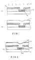
- a silicon oxide layer 102 providing an inter-layer insulating film and prepared by reacting SiH4 with 02 or N20 by means of plasma or heat, is formed on a semi-conductor substrate 101, which has transistors etc. provided thereon, to a thickness of about 0.3 to 0.6 micro-metres by means of gas phase growing. If flattening is required, it is desirable to provide a coating of glass, by means of spin coating, followed by heat treatment to improve the flatness.
- the silicon oxide layer 102 is patterned by dry etching using CHF3, for example, and a Ti photo-resist layer 103 as a mask to produce a contact hole 104.
- a Ti layer 105 is formed on the patterned layer 102 to a thickness of 20 nm by sputtering and a TiN layer 106 is formed contiguous with the Ti layer 105 to a thickness of 100 nm by means of reactive sputtering using a Ti target in a gas mixture of Ar and N2, or by means of sputtering using a TiN target.
- a dual layer structure comprising a Ti silicide layer 108 and a TiN layer 109, is generated in the contact region by fast heat treatment at a temperature from 600°C to 800°C in an N2 atmosphere at an 02 concentration of lower than 10 ppm.
- Si diffuses through into the grain boundary in the TiN layer 109 in the contact region.
- 0 atoms intrude slighly into the surface 110 of the TiN layer 109 due to the extremely low 02 concentration (lower than 10 ppm).
- an Al - 0.3% Cu layer 111 is formed to a thickness of 0.8 micro-metres on the TiN layer 109 by means of heat sputtering or bias sputtering at a temperature higher than 250°C.
- Si atoms contained in the TiN layer 109 in the contact region easily intrude into the Al - 0.3% Cu layer 111 to lower the melting point of the Al alloy and, at the same time, improve the wettability of the Al alloy.
- the oxygen in the TiN layer 109 and especially in the surface 110 thereof also improves the Al wettability, Al atoms can easily intrude into the contact region to provide satisfactory coverage even for a hole of sub-micron size with an aspect ratio greater than 1.
- the Si-containing TiN layer 109 prevents reaction between the Al alloy and the Si substrate.
- Figure 3 shows the results of measurement of the junction current leak with respect to a semi-conductor device in which rapid thermal annealing is not applied ( Figure 3 (a)) and a semi-conductor device according to the invention in which rapid thermal annealing is applied ( Figure 3 (b)).
- the device was subjected to fast heat treatment at 700°C for thirty seconds as described above.
- the device was subjected three times to thermal annealing at 450°C for thirty minutes after the formation of the Al - 0.3% Cu layer 111.
- the current was measured when a reverse bias voltage of 5V was applied to an N+ - P ⁇ junction.
- Figure 4 shows the results of measurements for electro-migration, in which the symbol “o” relates to devices which have not been subjected to rapid thermal annealing and the symbol " ⁇ " relates to an embodiment according to the present invention.
- the semi-conductor device according to the present invention has a working life increased by about one order of magnitude by comparison with the device which has not been subjected to rapid thermal annealing.
- FIG. 2 A further embodiment is shown in Figure 2. This embodiment corresponds with the embodiment of Figure 1 (and similar elements are designated by references numerals which are increased by 200) with the exception that a TiN layer 312 is formed to a thickness of 30 to 50 nm on the Al - 0.3% Cu layer 311 to provide an anti-reflection layer and thereby prevent halation during a photo-etching step in which the upper layers are formed into a desired connector pattern.
- Ti has been used for the layer which is subjected to rapid thermal annealing in the above embodiments
- W, Mo, Ta, etc. may also be used.
- Al - 0.3% Cu has been used as the Al alloy, another Al - Cu alloy, Al - Ti alloy, Al - Si alloy, etc. may also be employed.
- the present invention provides a highly reliable semi-conductor device, in which reaction between an Al alloy layer and an Si substrate and the disruption of contacts due to electro-migration are avoided, and which provides a close bond between the connector layers and the interlayer insulating film, and good step coverage of the Al alloy layer.
Landscapes
- Internal Circuitry In Semiconductor Integrated Circuit Devices (AREA)
Applications Claiming Priority (8)
| Application Number | Priority Date | Filing Date | Title |
|---|---|---|---|
| JP63196495A JP2764934B2 (ja) | 1988-08-06 | 1988-08-06 | 半導体装置 |
| JP196494/88 | 1988-08-06 | ||
| JP196495/88 | 1988-08-06 | ||
| JP63196494A JP2764933B2 (ja) | 1988-08-06 | 1988-08-06 | 半導体装置及びその製造方法 |
| JP196493/88 | 1988-08-06 | ||
| JP63196493A JP2764932B2 (ja) | 1988-08-06 | 1988-08-06 | 半導体装置及びその製造方法 |
| JP219819/88 | 1988-09-02 | ||
| JP63219819A JPH0268926A (ja) | 1988-09-02 | 1988-09-02 | 半導体装置の製造方法 |
Publications (2)
| Publication Number | Publication Date |
|---|---|
| EP0354717A2 true EP0354717A2 (de) | 1990-02-14 |
| EP0354717A3 EP0354717A3 (de) | 1990-06-13 |
Family
ID=27475811
Family Applications (1)
| Application Number | Title | Priority Date | Filing Date |
|---|---|---|---|
| EP89307849A Ceased EP0354717A3 (de) | 1988-08-06 | 1989-08-02 | Halbleiteranordnung und Verfahren zum Herstellen einer solchen Anordnung |
Country Status (3)
| Country | Link |
|---|---|
| US (2) | US4998157A (de) |
| EP (1) | EP0354717A3 (de) |
| KR (1) | KR950013737B1 (de) |
Cited By (6)
| Publication number | Priority date | Publication date | Assignee | Title |
|---|---|---|---|---|
| EP0459690A1 (de) * | 1990-05-31 | 1991-12-04 | AT&T Corp. | Verbindung einer integrierten Schaltung |
| US5268329A (en) * | 1990-05-31 | 1993-12-07 | At&T Bell Laboratories | Method of fabricating an integrated circuit interconnection |
| EP0690503A1 (de) * | 1994-05-31 | 1996-01-03 | Advanced Micro Devices, Inc. | Verbesserte Struktur einer Verbindungsleitung und Verfahren dafür |
| US5569961A (en) * | 1992-12-30 | 1996-10-29 | Samsung Electronics Co., Ltd. | Semiconductor device having a multi-layer metallization structure |
| WO1997006562A1 (en) * | 1995-08-10 | 1997-02-20 | Siemens Aktiengesellschaft | Metal interconnect structure for an integrated circuit with improved electromigration reliability |
| EP0740334B1 (de) * | 1995-04-27 | 2003-03-12 | Infineon Technologies AG | Verfahren zum isotropen Ätzen von Silizium, das hochselektiv gegenüber Wolfram ist |
Families Citing this family (42)
| Publication number | Priority date | Publication date | Assignee | Title |
|---|---|---|---|---|
| US5162262A (en) * | 1989-03-14 | 1992-11-10 | Mitsubishi Denki Kabushiki Kaisha | Multi-layered interconnection structure for a semiconductor device and manufactured method thereof |
| JPH038359A (ja) * | 1989-06-06 | 1991-01-16 | Fujitsu Ltd | 半導体装置の製造方法 |
| JPH07109829B2 (ja) * | 1989-11-20 | 1995-11-22 | 三菱電機株式会社 | 半導体装置の製造方法 |
| US5472912A (en) * | 1989-11-30 | 1995-12-05 | Sgs-Thomson Microelectronics, Inc. | Method of making an integrated circuit structure by using a non-conductive plug |
| US5478780A (en) * | 1990-03-30 | 1995-12-26 | Siemens Aktiengesellschaft | Method and apparatus for producing conductive layers or structures for VLSI circuits |
| JPH0430516A (ja) * | 1990-05-28 | 1992-02-03 | Canon Inc | 半導体装置及びその製造方法 |
| JPH05198525A (ja) * | 1992-01-21 | 1993-08-06 | Sony Corp | 配線構造及び配線の形成方法 |
| US5532031A (en) * | 1992-01-29 | 1996-07-02 | International Business Machines Corporation | I/O pad adhesion layer for a ceramic substrate |
| US5378660A (en) * | 1993-02-12 | 1995-01-03 | Applied Materials, Inc. | Barrier layers and aluminum contacts |
| JP3201061B2 (ja) * | 1993-03-05 | 2001-08-20 | ソニー株式会社 | 配線構造の製造方法 |
| JPH06268083A (ja) * | 1993-03-11 | 1994-09-22 | Sony Corp | 半導体装置の配線 |
| JP3216345B2 (ja) * | 1993-04-06 | 2001-10-09 | ソニー株式会社 | 半導体装置及びその作製方法 |
| KR960015564B1 (ko) * | 1993-04-16 | 1996-11-18 | 현대전자산업 주식회사 | 반도체 장치의 금속배선 형성방법 |
| US5412250A (en) * | 1993-09-24 | 1995-05-02 | Vlsi Technology, Inc. | Barrier enhancement at the salicide layer |
| US5429975A (en) * | 1993-10-25 | 1995-07-04 | United Microelectronics Corporation | Method of implanting during manufacture of ROM device |
| US5550084A (en) * | 1994-01-19 | 1996-08-27 | Advanced Micro Devices, Inc. | Integrated circuit fabrication using a metal silicide having a sputterdeposited metal nitride layer |
| US5514908A (en) * | 1994-04-29 | 1996-05-07 | Sgs-Thomson Microelectronics, Inc. | Integrated circuit with a titanium nitride contact barrier having oxygen stuffed grain boundaries |
| KR0147870B1 (ko) * | 1994-10-24 | 1998-11-02 | 문정환 | 반도체 소자의 콘택 전도층 형성방법 |
| US5614437A (en) * | 1995-01-26 | 1997-03-25 | Lsi Logic Corporation | Method for fabricating reliable metallization with Ta-Si-N barrier for semiconductors |
| US5612253A (en) * | 1995-01-31 | 1997-03-18 | Advanced Micro Devices, Inc. | Method for forming ordered titanium nitride and titanium silicide upon a semiconductor wafer using a three-step anneal process |
| KR0148325B1 (ko) * | 1995-03-04 | 1998-12-01 | 김주용 | 반도체 소자의 금속 배선 형성방법 |
| JP2754176B2 (ja) * | 1995-03-13 | 1998-05-20 | エルジイ・セミコン・カンパニイ・リミテッド | 緻密なチタン窒化膜及び緻密なチタン窒化膜/薄膜のチタンシリサイドの形成方法及びこれを用いた半導体素子の製造方法 |
| US5494860A (en) * | 1995-03-14 | 1996-02-27 | International Business Machines Corporation | Two step annealing process for decreasing contact resistance |
| DE69625265T2 (de) * | 1995-03-28 | 2003-09-04 | Texas Instruments Inc., Dallas | Halbleiterstrukturen |
| US5653019A (en) * | 1995-08-31 | 1997-08-05 | Regents Of The University Of California | Repairable chip bonding/interconnect process |
| US5776831A (en) * | 1995-12-27 | 1998-07-07 | Lsi Logic Corporation | Method of forming a high electromigration resistant metallization system |
| US6191032B1 (en) | 1997-02-04 | 2001-02-20 | Advanced Micro Devices, Inc. | Thin titanium film as self-regulating filter for silicon migration into aluminum metal lines |
| KR100241506B1 (ko) * | 1997-06-23 | 2000-03-02 | 김영환 | 반도체 소자의 금속 배선 형성 방법 |
| US6054768A (en) * | 1997-10-02 | 2000-04-25 | Micron Technology, Inc. | Metal fill by treatment of mobility layers |
| KR100457409B1 (ko) * | 1997-12-30 | 2005-02-23 | 주식회사 하이닉스반도체 | 반도체소자의금속배선형성방법 |
| US6376369B1 (en) | 1998-02-12 | 2002-04-23 | Micron Technology, Inc. | Robust pressure aluminum fill process |
| US6100186A (en) * | 1998-04-14 | 2000-08-08 | Micron Technology, Inc. | Method of selectively forming a contact in a contact hole |
| KR20000007410A (ko) * | 1998-07-03 | 2000-02-07 | 김영환 | 반도체 소자의 금속배선 형성방법 |
| US6117793A (en) * | 1998-09-03 | 2000-09-12 | Micron Technology, Inc. | Using silicide cap as an etch stop for multilayer metal process and structures so formed |
| US6207568B1 (en) | 1998-11-27 | 2001-03-27 | Taiwan Semiconductor Manufacturing Company | Ionized metal plasma (IMP) method for forming (111) oriented aluminum containing conductor layer |
| JP3353727B2 (ja) * | 1998-12-21 | 2002-12-03 | 日本電気株式会社 | 半導体装置の配線構造の形成方法 |
| US6080657A (en) * | 1999-07-16 | 2000-06-27 | Taiwan Semiconductor Manufacturing Company | Method of reducing AlCu hillocks |
| JP2001274143A (ja) * | 2000-03-28 | 2001-10-05 | Tdk Corp | ドライエッチング方法、微細加工方法及びドライエッチング用マスク |
| US8791572B2 (en) * | 2007-07-26 | 2014-07-29 | International Business Machines Corporation | Buried metal-semiconductor alloy layers and structures and methods for fabrication thereof |
| US9312121B1 (en) * | 2014-10-09 | 2016-04-12 | United Microelectronics Corporation | Method for cleaning contact hole and forming contact plug therein |
| US10153175B2 (en) | 2015-02-13 | 2018-12-11 | Taiwan Semiconductor Manufacturing Company, Ltd. | Metal oxide layered structure and methods of forming the same |
| US10236207B2 (en) * | 2016-06-20 | 2019-03-19 | Applied Materials, Inc. | Hydrogenation and nitridization processes for reducing oxygen content in a film |
Family Cites Families (28)
| Publication number | Priority date | Publication date | Assignee | Title |
|---|---|---|---|---|
| US3669730A (en) * | 1970-04-24 | 1972-06-13 | Bell Telephone Labor Inc | Modifying barrier layer devices |
| US4141022A (en) * | 1977-09-12 | 1979-02-20 | Signetics Corporation | Refractory metal contacts for IGFETS |
| USRE30412E (en) * | 1979-04-26 | 1980-10-07 | Eastman Kodak Company | CdTe Barrier type photovoltaic cells with enhanced open-circuit voltage, and process of manufacture |
| US4339869A (en) * | 1980-09-15 | 1982-07-20 | General Electric Company | Method of making low resistance contacts in semiconductor devices by ion induced silicides |
| JPS59175763A (ja) * | 1983-03-25 | 1984-10-04 | Fujitsu Ltd | 半導体装置 |
| FR2557712B1 (fr) * | 1983-12-30 | 1988-12-09 | Trt Telecom Radio Electr | Processeur pour traiter des donnees en fonction d'instructions provenant d'une memoire-programme |
| US4700465A (en) * | 1984-01-27 | 1987-10-20 | Zoran Corporation | Method of selectively making contact structures both with barrier metal and without barrier metal in a single process flow |
| US4829363A (en) * | 1984-04-13 | 1989-05-09 | Fairchild Camera And Instrument Corp. | Structure for inhibiting dopant out-diffusion |
| US4640004A (en) * | 1984-04-13 | 1987-02-03 | Fairchild Camera & Instrument Corp. | Method and structure for inhibiting dopant out-diffusion |
| JPS61183942A (ja) * | 1985-02-08 | 1986-08-16 | Fujitsu Ltd | 半導体装置の製造方法 |
| JPS61208869A (ja) * | 1985-03-14 | 1986-09-17 | Nec Corp | 半導体装置及びその製造方法 |
| CN1012310B (zh) * | 1985-05-01 | 1991-04-03 | 得克萨斯仪器公司 | 超大规模集成电路的局部互连方法及其结构 |
| US4676866A (en) * | 1985-05-01 | 1987-06-30 | Texas Instruments Incorporated | Process to increase tin thickness |
| US4890141A (en) * | 1985-05-01 | 1989-12-26 | Texas Instruments Incorporated | CMOS device with both p+ and n+ gates |
| US4713358A (en) * | 1986-05-02 | 1987-12-15 | Gte Laboratories Incorporated | Method of fabricating recessed gate static induction transistors |
| JP2658019B2 (ja) * | 1986-07-03 | 1997-09-30 | ソニー株式会社 | 半導体装置の製造方法 |
| US4782380A (en) * | 1987-01-22 | 1988-11-01 | Advanced Micro Devices, Inc. | Multilayer interconnection for integrated circuit structure having two or more conductive metal layers |
| US4884123A (en) * | 1987-02-19 | 1989-11-28 | Advanced Micro Devices, Inc. | Contact plug and interconnect employing a barrier lining and a backfilled conductor material |
| KR920002350B1 (ko) * | 1987-05-21 | 1992-03-21 | 마쯔시다덴기산교 가부시기가이샤 | 반도체장치의 제조방법 |
| JPS63314850A (ja) * | 1987-06-18 | 1988-12-22 | Fujitsu Ltd | 半導体装置 |
| US4784973A (en) * | 1987-08-24 | 1988-11-15 | Inmos Corporation | Semiconductor contact silicide/nitride process with control for silicide thickness |
| JP2776826B2 (ja) * | 1988-04-15 | 1998-07-16 | 株式会社日立製作所 | 半導体装置およびその製造方法 |
| US4990997A (en) * | 1988-04-20 | 1991-02-05 | Fujitsu Limited | Crystal grain diffusion barrier structure for a semiconductor device |
| US5084417A (en) * | 1989-01-06 | 1992-01-28 | International Business Machines Corporation | Method for selective deposition of refractory metals on silicon substrates and device formed thereby |
| US5196360A (en) * | 1990-10-02 | 1993-03-23 | Micron Technologies, Inc. | Methods for inhibiting outgrowth of silicide in self-aligned silicide process |
| US5242860A (en) * | 1991-07-24 | 1993-09-07 | Applied Materials, Inc. | Method for the formation of tin barrier layer with preferential (111) crystallographic orientation |
| US5240880A (en) * | 1992-05-05 | 1993-08-31 | Zilog, Inc. | Ti/TiN/Ti contact metallization |
| US5187120A (en) * | 1992-08-24 | 1993-02-16 | Hewlett-Packard Company | Selective deposition of metal on metal nitride to form interconnect |
-
1989
- 1989-08-01 US US07/387,834 patent/US4998157A/en not_active Expired - Lifetime
- 1989-08-02 EP EP89307849A patent/EP0354717A3/de not_active Ceased
- 1989-08-03 KR KR1019890011087A patent/KR950013737B1/ko not_active Expired - Fee Related
-
1992
- 1992-04-01 US US07/863,462 patent/US5312772A/en not_active Expired - Lifetime
Non-Patent Citations (3)
| Title |
|---|
| IEEE TRANSACTIONS ON ELECTRON DEVICES, vol. ED-34, no. 3, March 1987, pages 599-606, IEEE, New York, US; T. MAEDA et al.: "A highly reliable interconnection for a BF+2-implanted junction utilizing a TiN/Ti barrier metal system" * |
| JOURNAL OF VACUUM SCIENCE & TECHNOLOGY/A, vol. 4, no. 3, part 1, May-June 1986, pages 993-997, American Vacuum Society, Woodbury, NY, US; L.J. BRILLSON et al.: "Titanium-silicon and silicon dioxide reactions controlled by low temperature rapid thermal annealing" * |
| SOLID STATE TECHNOLOGY, vol. 28, no. 10, October 1985, pages 161-166, Port Washington, New York, US; J.R. SHAPPIRIO: "Diffusion barriers in advanced semiconductor device technology" * |
Cited By (8)
| Publication number | Priority date | Publication date | Assignee | Title |
|---|---|---|---|---|
| EP0459690A1 (de) * | 1990-05-31 | 1991-12-04 | AT&T Corp. | Verbindung einer integrierten Schaltung |
| US5268329A (en) * | 1990-05-31 | 1993-12-07 | At&T Bell Laboratories | Method of fabricating an integrated circuit interconnection |
| US5569961A (en) * | 1992-12-30 | 1996-10-29 | Samsung Electronics Co., Ltd. | Semiconductor device having a multi-layer metallization structure |
| EP0690503A1 (de) * | 1994-05-31 | 1996-01-03 | Advanced Micro Devices, Inc. | Verbesserte Struktur einer Verbindungsleitung und Verfahren dafür |
| US5675186A (en) * | 1994-05-31 | 1997-10-07 | Advanced Micro Devices, Inc. | Construction that prevents the undercut of interconnect lines in plasma metal etch systems |
| US5688717A (en) * | 1994-05-31 | 1997-11-18 | Advanced Micro Devices, Inc. | Construction that prevents the undercut of interconnect lines in plasma metal etch systems |
| EP0740334B1 (de) * | 1995-04-27 | 2003-03-12 | Infineon Technologies AG | Verfahren zum isotropen Ätzen von Silizium, das hochselektiv gegenüber Wolfram ist |
| WO1997006562A1 (en) * | 1995-08-10 | 1997-02-20 | Siemens Aktiengesellschaft | Metal interconnect structure for an integrated circuit with improved electromigration reliability |
Also Published As
| Publication number | Publication date |
|---|---|
| US4998157A (en) | 1991-03-05 |
| US5312772A (en) | 1994-05-17 |
| KR900003998A (ko) | 1990-03-27 |
| KR950013737B1 (ko) | 1995-11-15 |
| EP0354717A3 (de) | 1990-06-13 |
Similar Documents
| Publication | Publication Date | Title |
|---|---|---|
| EP0354717A2 (de) | Halbleiteranordnung und Verfahren zum Herstellen einer solchen Anordnung | |
| EP0516279B1 (de) | Verbindungsstruktur einer Halbleiteranordnung und ein Herstellungsverfahren dafür | |
| JP2700103B2 (ja) | 改良された集積回路構造および改良された集積回路構造を形成する方法 | |
| JP2915828B2 (ja) | 半導体の配線構造およびその製造方法 | |
| EP0499433A2 (de) | Halbleiter-Vorrichtung mit Verdrahtung der verbesserten Zuverlässigkeit und Verfahren zu ihner Herstellung | |
| KR920005701B1 (ko) | 반도체 집적회로 내의 소자 연결용 금속배선층 및 그 제조방법 | |
| JPS5846192B2 (ja) | 接点構造体 | |
| JPS61183942A (ja) | 半導体装置の製造方法 | |
| EP0542262A1 (de) | Verfahren zur Bildung eines Metalleiters für ein Halbleiterbauelement | |
| US4916397A (en) | Semiconductor device with bonding pad | |
| JPH05102155A (ja) | 銅配線構造体及びその製造方法 | |
| US4745089A (en) | Self-aligned barrier metal and oxidation mask method | |
| US5528081A (en) | High temperature refractory metal contact in silicon integrated circuits | |
| IE54310B1 (en) | Multilayer electrode of a semiconductor device | |
| JPH06204170A (ja) | 半導体装置およびその製造方法 | |
| JP3128961B2 (ja) | 半導体装置及びその製造方法 | |
| US20030006504A1 (en) | Contact structure, method of forming the same, semiconductor device, and method of manufacturing the same | |
| US6004877A (en) | Method of forming a tungsten layer with N2 plasma treatment | |
| KR100327092B1 (ko) | 반도체 소자의 구리 합금배선 형성방법 | |
| US5350711A (en) | Method of fabricating high temperature refractory metal nitride contact and interconnect structure | |
| JP3120471B2 (ja) | 半導体装置の製造方法 | |
| JP3230909B2 (ja) | 半導体装置およびその製造方法 | |
| JPH05102154A (ja) | 半導体装置 | |
| JP2764934B2 (ja) | 半導体装置 | |
| JPS62165342A (ja) | 半導体装置 |
Legal Events
| Date | Code | Title | Description |
|---|---|---|---|
| PUAI | Public reference made under article 153(3) epc to a published international application that has entered the european phase |
Free format text: ORIGINAL CODE: 0009012 |
|
| AK | Designated contracting states |
Kind code of ref document: A2 Designated state(s): DE FR GB NL |
|
| PUAL | Search report despatched |
Free format text: ORIGINAL CODE: 0009013 |
|
| AK | Designated contracting states |
Kind code of ref document: A3 Designated state(s): DE FR GB NL |
|
| 17P | Request for examination filed |
Effective date: 19901120 |
|
| 17Q | First examination report despatched |
Effective date: 19920723 |
|
| STAA | Information on the status of an ep patent application or granted ep patent |
Free format text: STATUS: THE APPLICATION HAS BEEN REFUSED |
|
| 18R | Application refused |
Effective date: 19941209 |