EP0355922A1 - Circuit d'entrée à commutation accélérée - Google Patents
Circuit d'entrée à commutation accélérée Download PDFInfo
- Publication number
- EP0355922A1 EP0355922A1 EP89202109A EP89202109A EP0355922A1 EP 0355922 A1 EP0355922 A1 EP 0355922A1 EP 89202109 A EP89202109 A EP 89202109A EP 89202109 A EP89202109 A EP 89202109A EP 0355922 A1 EP0355922 A1 EP 0355922A1
- Authority
- EP
- European Patent Office
- Prior art keywords
- transistor
- base
- collector
- ref
- point
- Prior art date
- Legal status (The legal status is an assumption and is not a legal conclusion. Google has not performed a legal analysis and makes no representation as to the accuracy of the status listed.)
- Granted
Links
- 101150109657 ureF gene Proteins 0.000 abstract 1
- 102220502002 U3 small nucleolar RNA-interacting protein 2_R10S_mutation Human genes 0.000 description 3
- 102220534634 Aryl hydrocarbon receptor nuclear translocator-like protein 1_R11I_mutation Human genes 0.000 description 1
- 230000000295 complement effect Effects 0.000 description 1
- 230000000694 effects Effects 0.000 description 1
- 238000000034 method Methods 0.000 description 1
- 238000004377 microelectronic Methods 0.000 description 1
- 230000001052 transient effect Effects 0.000 description 1
- 230000007704 transition Effects 0.000 description 1
Images
Classifications
-
- H—ELECTRICITY
- H03—ELECTRONIC CIRCUITRY
- H03K—PULSE TECHNIQUE
- H03K17/00—Electronic switching or gating, i.e. not by contact-making and –breaking
- H03K17/04—Modifications for accelerating switching
-
- H—ELECTRICITY
- H03—ELECTRONIC CIRCUITRY
- H03K—PULSE TECHNIQUE
- H03K3/00—Circuits for generating electric pulses; Monostable, bistable or multistable circuits
- H03K3/02—Generators characterised by the type of circuit or by the means used for producing pulses
- H03K3/26—Generators characterised by the type of circuit or by the means used for producing pulses by the use, as active elements, of bipolar transistors with internal or external positive feedback
- H03K3/28—Generators characterised by the type of circuit or by the means used for producing pulses by the use, as active elements, of bipolar transistors with internal or external positive feedback using means other than a transformer for feedback
- H03K3/281—Generators characterised by the type of circuit or by the means used for producing pulses by the use, as active elements, of bipolar transistors with internal or external positive feedback using means other than a transformer for feedback using at least two transistors so coupled that the input of one is derived from the output of another, e.g. multivibrator
- H03K3/286—Generators characterised by the type of circuit or by the means used for producing pulses by the use, as active elements, of bipolar transistors with internal or external positive feedback using means other than a transformer for feedback using at least two transistors so coupled that the input of one is derived from the output of another, e.g. multivibrator bistable
- H03K3/2893—Bistables with hysteresis, e.g. Schmitt trigger
Definitions
- the invention relates to a switching input circuit having a stage of the coupled transmitter type (ECL) with two transistors, the first receiving on its base an input signal and the second receiving on its base a control signal, which is produced by a control circuit from the signal from the collector of the first transistor, so as to obtain on the collector of the second transistor an output signal switching faster than the input signal.
- ECL coupled transmitter type
- Such a circuit generally used to compensate for the switching slowdown due to highly capacitive input lines, is known from MOTOROLA's "Microelectronic Cell Data Book", the control circuit consisting of a simple resistive divider bridge between the collector of the first transistor, the base of the second transistor and the ground.
- MOTOROLA Metal Organic Cell Data Book
- the control circuit consisting of a simple resistive divider bridge between the collector of the first transistor, the base of the second transistor and the ground.
- the present invention provides an input circuit of the aforementioned type in which the value and the amplitude of the control voltage can be chosen.
- the circuit according to the invention is for this purpose characterized in that the control circuit comprises a third transistor whose collector is connected to a supply voltage source, the base of which is connected to the collector of the first transistor and in that '' it successively includes a first, a second and a third resistance arranged in series between the emitter of the third transistor and a reference point to which a reference voltage source and a first reference current source are connected, the point common to the first and to the second resistor being connected to a second source of reference current, and the point common to the second and to the third resistance delivering said control signal.
- the control circuit comprises a third transistor whose collector is connected to a supply voltage source, the base of which is connected to the collector of the first transistor and in that '' it successively includes a first, a second and a third resistance arranged in series between the emitter of the third transistor and a reference point to which a reference voltage source and a first reference current source are connected, the point common to the first and to the second resistor being connected to a second source
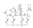
- the circuit comprises an input follower stage comprising a transistor T1 receiving on its base input signals e, and producing on an emitter signals E, this emitter being conventionally connected to a current source (T2, R2) .
- This buffer stage is conventional and has only an optional decoupling function.
- the actual input circuit comprises a gate of the type with coupled emitters (ECL) comprising two transistors T3 and T4 whose coupled emitters are connected to a current source (R5, T5) of intensity I d'int.
- the collectors of the transistors T3 and T4 are connected to a supply voltage source V c through resistors R3 and R4 respectively.
- the base of transistor T3 receives the signal E from the first emitter of transistor T1.
- the output signal S is that supplied by the collector of transistor T4, the collector of transistor T3 providing the complementary signal S .
- the base voltage of transistor T4 is determined from the collector voltage of transistor T3. With regard to the prior art, we have already specified that this was done by potentiometrically dividing the collector voltage of the transistor T3. This has the disadvantage of considerably limiting the control of the effect thus produced. We can thus choose the central value of the base voltage of transistor T4, but at this time, the amplitude of its varia cannot be chosen. On the other hand, if one wants to choose the amplitude of the amplitude of this variation, then the central value cannot be it and in any case, the value of this amplitude is limited to a fraction of the switching amplitude ⁇ V of the ECL door.
- the base of a transistor T6 is connected to the collector of the transistor T3.
- the collector of transistor T6 is connected to a supply voltage voltage V c , and its emitter is connected to a point C through three resistors in series respectively R10, R11 and R12, a direct diode T10 possibly being interposed between l emitter of transistor T10 and resistance R10 so as to achieve level compensation.
- the point A common to resistors R10 and R11 is connected to a current source (R8, T8) of intensity I c .
- the point B common to the resistors R11 and R12 is connected to the base of the transistor T4, possibly through a resistor R4.
- the aforementioned point C, another end of the resistor R12 is connected to a reference voltage source U REF .
- This reference voltage source includes a transistor T7 whose collector is connected to the supply voltage source V c , whose base receives a reference voltage (V c -V REF ), and whose emitter is connected to the point C as well as a current source (R9, T9) of intensity I D.
- This value ⁇ V of the switching amplitude is fixed by the standards defining the circuit (800mV for ECL).
- the third state is a state of transient equilibrium.
- the voltage on the emitter of the transistor T10 (point O) is at the high level which is greater than the voltage at the point C and all of the current I c passes through the resistor R10 .
- the voltage at point O is at the low level which is less than the voltage at point C
- the voltage at point A is less than that at point C
- the current I c is divided between the two branches R10 and (R11, R12). This is what makes it possible to adjust the amplitude of the voltage variation on the basis of the transistor T4 and therefore to use the input circuit for values different from ⁇ V.
- V BE6 base-emitter voltage of transistor T6
- V BE7 base-emitter voltage of transistor T7
- V BE6 + V D + I10R10) V c - V REF - V BE7 + I11 (R11 + R12) I11 designating the current passing through the resistors R11 and R12.
- Equations (2 ′) and (8) allow the values of the elements of the input circuit to be chosen as a function of both the switching amplitude ⁇ V of the coupled transmitter stage and the central switching value E0 on the base of transistor T3.
- V D 0.75V
- R10 1k ⁇
- 112.5mV
Landscapes
- Engineering & Computer Science (AREA)
- Power Engineering (AREA)
- Electronic Switches (AREA)
- Logic Circuits (AREA)
- Manipulation Of Pulses (AREA)
- Amplifiers (AREA)
Abstract
Description
- L'invention concerne un circuit d'entrée de commutation présentant un étage du type à émetteurs couplés (ECL) à deux transistors, le premier recevant sur sa base un signal d'entrée et le deuxième recevant sur sa base un signal de commande, lequel est élaboré par un circuit de commande à partir du signal du collecteur du premier transistor, de manière à obtenir sur le collecteur du deuxième transistor un signal de sortie commutant plus rapidement que le signal d'entrée.
- Un tel circuit, généralement utilisé pour compenser le ralentissement de commutation dû à des lignes d'entrée fortement capacitives, est connu du "Microelectronic Cell Data Book" de MOTOROLA, le circuit de commande consistant en un simple pont diviseur résistif entre le collecteur du premier transistor, la base du deuxième transistor et la masse. Lorsque par exemple la tension E passe d'un état bas à un état haut, la mise en conduction du premier transistor entraîne la baisse de la tension sur la base du deuxième transistor, ce qui accélère la commutation. Ce phénomène est le même, en sens inverse, pour une transition du signal E d'un état haut à un état bas. La dépendance directe entre la tension de commande et le signal du collecteur du premier transistor fait qu'il n'est pas possible de choisir tous les paramètres de fonctionnement.
- La présente invention propose un circuit d'entrée du type précité dans lequel la valeur et l'amplitude de la tension de commande peuvent être choisies.
- Le circuit selon l'invention est dans ce but caractérisé en ce que le circuit de commande comporte un troisième transistor dont le collecteur est connecté à une source de tension d'alimentation, dont la base est connectée au collecteur du premier transistor et en ce qu'il comporte successivement une première, une deuxième et une troisième résistance disposées en série entre l'émetteur du troisième transistor et un point de référence auxquels sont connectés une source de tension de référence et une première source de courant de référence, le point commun à la première et à la deuxième résistance étant connecté à une deuxième source de courant de référence, et le point commun à la deuxième et à la troisième résistance délivrant ledit signal de commande.
- L'invention sera mieux comprise à la lecture de la description qui va suivre en liaison avec la figure unique qui représente le mode de réalisation préféré de l'invention.
- Le circuit comporte un étage suiveur d'entrée comportant un transistor T₁ recevant sur sa base des signaux d'entrée e, et produisant sur un émetteur des signaux E, cet émetteur étant connecté de manière classique à une source de courant (T₂,R₂). Cet étage tampon est classique et n'a qu'une fonction facultative de découplage. Le circuit d'entrée proprement dit comporte une porte du type à émetteurs couplés (ECL) comprenant deux transistors T₃ et T₄ dont les émetteurs couplés sont connectés à une source de courant (R₅,T₅) d'intensité I₁. Les collecteurs des transistors T₃ et T₄ sont reliés à une source de tension d'alimentation Vc à travers des résistances respectivement R₃ et R₄. La base du transistor T₃ reçoit le signal E du premier émetteur du transistor T₁. Le signal de sortie S est celui fourni par le collecteur du transistor T₄, le collecteur du transistor T₃ fournissant le signal complémentaire
S . - La tension de base du transistor T₄ est déterminée à partir de la tension de collecteur du transistor T₃. En ce qui concerne l'art antérieur, nous avons déjà précisé que cela était effectué en divisant potentiométriquement la tension de collecteur du transistor T₃. Ceci a pour inconvénient de limiter considérablement le contrôle de l'effet ainsi produit. On peut ainsi choisir la valeur centrale de la tension de base du transistor T₄, mais à ce moment là, l'amplitude de sa varia tion ne peut être choisie. Par contre, si on veut choisir l'amplitude de l'amplitude de cette variation, alors la valeur centrale ne peut l'être et de toutes façons, la valeur de cette amplitude est limitée à une fraction de l'amplitude de commutation ΔV de la porte ECL.
- Le circuit qui va maintenant être décrit permet de choisir les deux paramètres et de plus dans une gamme de valeurs aussi large que désirée.
- La base d'un transistor T₆ est connectée au collecteur du transistor T₃. Le collecteur du transistor T₆ est connecté à une tension de tension d'alimentation Vc, et son émetteur est relié à un point C à travers trois résistances en série respectivement R₁₀, R₁₁ et R₁₂, une diode en direct T₁₀ étant éventuellement intercalée entre l'émetteur du transistor T₁₀ et la résistance R₁₀ de manière à réaliser une compensation de niveau. Le point A commun aux résistances R₁₀ et R₁₁ est connecté à une source de courant (R₈,T₈) d'intensité Ic. Le point B commun aux résistances R₁₁ et R₁₂ est connecté à la base du transistor T₄, éventuellement à travers une résistance R₄. Le point C précité, autre extrémité de la résistance R₁₂ est connecté à une source de tension de référence UREF. Cette source de tension de référence comporte un transistor T₇ dont le collecteur est connecté à la source de tension d'alimentation Vc, dont la base reçoit une tension de référence (Vc-VREF), et dont un émetteur est connecté au point C ainsi qu'à une source de courant (R₉,T₉) d'intensité ID. Ce courant ID assure que notamment ledit émetteur soit toujours traversé par un courant Ir, de telle sorte que l'on ait toujours :
UREF = Vc- VREF - VBE
VBE désignant la tension base-émetteur d'un transistor, soit environ 0,7V. - On peut distinguer trois états principaux. Lorsque le signal d'entrée E est au niveau bas (premier état), le transistor T₃ est bloqué et le collecteur du transistor T₃ est est à la tension Vc. Lorsque le signal E est au niveau haut (deuxième état), le transistor T₃ est passant et le collecteur du transistor T₃ est à la tension Vc-ΔV avec :
ΔV = R₃I₁ - Cette valeur ΔV de l'amplitude de commutation est fixée par les normes définissant le circuit (800mV pour de l'ECL).
- Le troisième état est un état d'équilibre transitoire.
- Dans le premier état (E au niveau bas), la tension sur l'émetteur du transistor T₁₀ (point O) est au niveau haut qui est supérieur à la tension au point C et la totalité du courant Ic passe à travers la résistance R₁₀. Dans le deuxième état (E au niveau haut), la tension au point O est au niveau bas qui est inférieur à la tension au point C, la tension au point A est inférieure à celle au point C et le courant Ic se divise entre les deux branches R₁₀ et (R₁₁, R₁₂). C'est ce qui permet d'effectuer un réglage de l'amplitude de variation de tension sur la base du transistor T₄ et donc d'utiliser le circuit d'entrée pour des valeurs différentes de ΔV. Dans le troisième état, les tensions au point A et au point C sont égales, il n'y a pas de courant dans la branche (R₁₁, R₁₂) et la tension au point B a donc la valeur UREF, qui doit, pour un fonctionnement symétrique, être égale à la valeur E₀ du signal d'entrée E à mi-pente.
- On a dans ce cas :
E₀ = UREF = Vc - VREF - VD
d'où on déduit la valeur de VREF
VREF = Vc -VD - E₀ - On va maintenant décrire un mode de calcul des élément du circuit permettant d'obtenir en fonctionnement symétrique.
- Pour un fonctionnement symétrique, on choisit que le circuit soit dans le troisième état pour une demi-amplitude de commutation soit :
S = Vc -
- La relation d'équilibre s'écrit alors :
Vc
avec VD : chute de tension dans une diode
VBE6 : tension base-émetteur du transistor T₆
VBE7 : tension base-émetteur du transistor T₇ - Les transistors T₆ et T₇ étant traversés respectivement par Ic et ID, (Ir=ID), on obtient la première condition :

- On a tout intérêt à choisir Ic = ID, d'où :
R₁₀Ic = VREF -
d'où :
R₁₀Ic = Vc - 2VD - E₀-
- Dans le premier état, on a (en écrivant l'égalité des tensions au point A)
Vc-(VBE6 + VD + I₁₀R₁₀) = Vc - VREF - VBE7 + I₁₁(R₁₁+R₁₂)
I₁₁ désignant le courant traversant les résistances R₁₁ et R₁₂.
Soit VBE6 +VD + I₁₀R₁₀ + I₁₁(R₁₁+R₁₂) = VREF + VBE7
et
I₁₀ = Ic + I₁₁ ; I₁₁ + IR = ID
D'où :
VBE6 + VD +(Ic+ID-IR)R₁₀+(ID - IR)(R₁₁+R₁₂)= VREF + VBE7 - Les transistors T₆ et T₇ étant parcourus par des courants égaux respectivement à Ic+ ID- IRet IR, on obtient la deuxième condition.

- On peut choisir le rapport n entre ID et IR, soit par exemple 2.
- On a alors pour n=2 et Ic=ID

- Dans le deuxième état, le courant I₁₁ circule dans l'autre sens et le courant Ic se divise entre R₁₀ d'une part et R₁₁ et R₁₂ d'autre part :
Vc-ΔV - (VBE6+VD+I₁₀R₁₀) = Vc-VREF-VBE7-I₁₁(R₁₁+R₁₂)
soit
ΔV+VBE6+ VD+ I₁₀R₁₀ = VREF+VBE7+ I₁₁(R₁₁+R₁₂).
I₁₀ + I₁₁ = Ic
IR = ID + I₁₁
d'où :
- On choisit

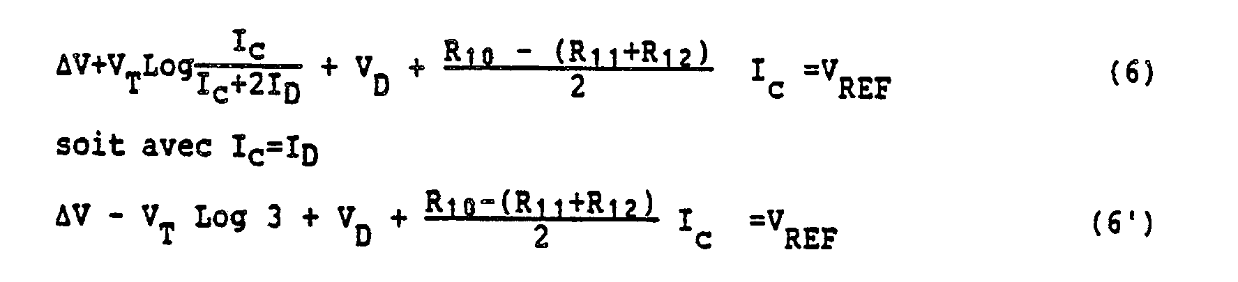
- En rapprochant les équations (4) et (6′), il vient :
(R₁₀ + R₁₁ + R₁₂) Ic = ΔV - 2 VT Log 3 (7) - En utilisant l'équation (2′), on a alors :
(R₁₁ + R₁₂)Ic =
- Les équations (2′) et (8) permettent de choisir les valeurs des éléments du circuit d'entrée en fonction à la fois de l'amplitude de commutation ΔV de l'étage à émetteur couplés et de la valeur centrale de commutation E₀ sur la base du transistor T₃.
- Il est en outre possible de choisir la valeur de l'écart |VB-EO| dans le premier et le deuxième état. Cet écart est le même dans ces deux états, car on a choisi un fonctionnement symétrique (voir plus haut).
- Dans le premier état, on a :

- En remplaçant R₁₀ Ic par sa valeur tirée de (2′), et Vc-EO par VREF + VD, on obtient :

- En choisissant la valeur de R₁₁Ic, on choisit |VB-EO| , donc l'amplitude du signal de commande.
- VREF = 1,3V
ΔV = 600 mV
Ic = ID = 250µA
VD = 0,75V
R₁₀ = 1kΩ
R₁₁ = R₁₂ = 500Ω
|VB-EO| = 112,5mV
Claims (3)
Applications Claiming Priority (2)
| Application Number | Priority Date | Filing Date | Title |
|---|---|---|---|
| FR8811033 | 1988-08-19 | ||
| FR8811033A FR2635620B1 (fr) | 1988-08-19 | 1988-08-19 | Circuit d'entree a commutation acceleree |
Publications (2)
| Publication Number | Publication Date |
|---|---|
| EP0355922A1 true EP0355922A1 (fr) | 1990-02-28 |
| EP0355922B1 EP0355922B1 (fr) | 1993-06-16 |
Family
ID=9369416
Family Applications (1)
| Application Number | Title | Priority Date | Filing Date |
|---|---|---|---|
| EP89202109A Expired - Lifetime EP0355922B1 (fr) | 1988-08-19 | 1989-08-17 | Circuit d'entrée à commutation accélérée |
Country Status (7)
| Country | Link |
|---|---|
| US (1) | US4972103A (fr) |
| EP (1) | EP0355922B1 (fr) |
| JP (1) | JP2911494B2 (fr) |
| KR (1) | KR900004107A (fr) |
| DE (1) | DE68907151T2 (fr) |
| FR (1) | FR2635620B1 (fr) |
| HK (1) | HK20495A (fr) |
Cited By (1)
| Publication number | Priority date | Publication date | Assignee | Title |
|---|---|---|---|---|
| US9647307B2 (en) | 2012-04-28 | 2017-05-09 | Huawei Technologies Co., Ltd. | Tunable filter and duplexer including filter |
Families Citing this family (5)
| Publication number | Priority date | Publication date | Assignee | Title |
|---|---|---|---|---|
| US5068552A (en) * | 1990-09-10 | 1991-11-26 | Kabushiki Kaisha Toshiba | Voltage follower circuit having improved dynamic range |
| USRE34771E (en) * | 1989-09-11 | 1994-11-01 | Kabushiki Kaisha Toshiba | Voltage follower circuit having improved dynamic range |
| KR930008554A (ko) * | 1991-10-25 | 1993-05-21 | 김광호 | 콤페레이터 |
| JPH0637626A (ja) * | 1992-03-27 | 1994-02-10 | Toshiba Corp | バイアス電流供給回路 |
| US5945848A (en) * | 1996-11-19 | 1999-08-31 | Rockwell Semiconductor Systems, Inc. | Effectively differential, multiple input OR/NOR gate architecture |
Citations (2)
| Publication number | Priority date | Publication date | Assignee | Title |
|---|---|---|---|---|
| US3646361A (en) * | 1970-10-16 | 1972-02-29 | Hughes Aircraft Co | High-speed sample and hold signal level comparator |
| EP0192907A1 (fr) * | 1984-12-28 | 1986-09-03 | Fujitsu Limited | Dispositif semi-conducteur ayant une partie d'entrée de signaux |
Family Cites Families (6)
| Publication number | Priority date | Publication date | Assignee | Title |
|---|---|---|---|---|
| FR1594389A (fr) * | 1967-12-20 | 1970-06-01 | ||
| US3694198A (en) * | 1971-02-19 | 1972-09-26 | Mallory & Co Inc P R | Silver-cadmium oxide alloys having periodic precipitation |
| DE3217512A1 (de) * | 1982-05-10 | 1983-11-10 | Siemens AG, 1000 Berlin und 8000 München | Schaltungsanordnung zur pegelumsetzung |
| JPS61264909A (ja) * | 1985-05-20 | 1986-11-22 | Fujitsu Ltd | シユミツトトリガ回路 |
| JPS62264909A (ja) * | 1986-05-14 | 1987-11-17 | 松下電工株式会社 | 電動ろくろ |
| US4835455A (en) * | 1988-09-15 | 1989-05-30 | Honeywell Inc. | Reference voltage generator |
-
1988
- 1988-08-19 FR FR8811033A patent/FR2635620B1/fr not_active Expired - Fee Related
-
1989
- 1989-07-28 US US07/387,454 patent/US4972103A/en not_active Expired - Fee Related
- 1989-08-16 KR KR1019890011630A patent/KR900004107A/ko not_active Ceased
- 1989-08-17 EP EP89202109A patent/EP0355922B1/fr not_active Expired - Lifetime
- 1989-08-17 DE DE89202109T patent/DE68907151T2/de not_active Expired - Fee Related
- 1989-08-18 JP JP1211533A patent/JP2911494B2/ja not_active Expired - Lifetime
-
1995
- 1995-02-16 HK HK20495A patent/HK20495A/xx not_active IP Right Cessation
Patent Citations (2)
| Publication number | Priority date | Publication date | Assignee | Title |
|---|---|---|---|---|
| US3646361A (en) * | 1970-10-16 | 1972-02-29 | Hughes Aircraft Co | High-speed sample and hold signal level comparator |
| EP0192907A1 (fr) * | 1984-12-28 | 1986-09-03 | Fujitsu Limited | Dispositif semi-conducteur ayant une partie d'entrée de signaux |
Non-Patent Citations (3)
| Title |
|---|
| ELEKTRONIK, vol. 35, no. 12, 13 juin 1986, page 120; H. PELKA: "Schmitt-Trigger-Inverter mit einstellbarer Hysterese" * |
| IEEE JOURNAL OF SOLID-STATE CIRCUITS, vol. SC-17, no. 6, décembre 1982, IEEE, New York, US; E.J. DICKES et al.: "A graphical analysis of the Schmitt trigger circuit" * |
| PATENT ABSTRACTS OF JAPAN, vol. 11, no. 117 (E-498)[2564], 11 avril 1987, page 159 E 498; & JP-A-61 264 910 (FUJITSU LTD) 22-11-1986 * |
Cited By (1)
| Publication number | Priority date | Publication date | Assignee | Title |
|---|---|---|---|---|
| US9647307B2 (en) | 2012-04-28 | 2017-05-09 | Huawei Technologies Co., Ltd. | Tunable filter and duplexer including filter |
Also Published As
| Publication number | Publication date |
|---|---|
| HK20495A (en) | 1995-02-24 |
| US4972103A (en) | 1990-11-20 |
| EP0355922B1 (fr) | 1993-06-16 |
| DE68907151T2 (de) | 1994-01-05 |
| FR2635620A1 (fr) | 1990-02-23 |
| KR900004107A (ko) | 1990-03-27 |
| JPH02101812A (ja) | 1990-04-13 |
| FR2635620B1 (fr) | 1991-08-02 |
| DE68907151D1 (de) | 1993-07-22 |
| JP2911494B2 (ja) | 1999-06-23 |
Similar Documents
| Publication | Publication Date | Title |
|---|---|---|
| EP0414319B1 (fr) | Circuit destiné à fournir une tension de référence | |
| EP0562916B1 (fr) | Dispositif de génération de tensions de référence | |
| KR0152701B1 (ko) | 감쇠 귀환형 차동증폭기 | |
| FR2676149A1 (fr) | Amplificateur differentiel notamment du type a cascode. | |
| EP0296762A2 (fr) | Amplificateur opérationnel de transconductance utilisé dans des circuits d'échantillonnage et de mémoire et circuits comparables | |
| FR2589649A1 (fr) | Dispositif destine a augmenter la puissance de sortie d'un appareil radioelectrique alimente a basse tension, par exemple du type autoradio | |
| EP0587509B1 (fr) | Circuit convertisseur tension/courant | |
| FR2535552A1 (fr) | Appareil et procede pour la synthese d'un signal d'excitation destine au test actif d'un circuit integre | |
| EP0355922B1 (fr) | Circuit d'entrée à commutation accélérée | |
| EP0649079A1 (fr) | Circuit générateur de tension stabilisée du type bandgap | |
| US4472678A (en) | Test apparatus for circuits having a multiplex input/output terminal including a load connected to the terminal together with circuitry for monitoring the current flow through the load when inputting a signal to the terminal | |
| US5874861A (en) | Amplifier circuit | |
| US4533844A (en) | Peak storage amplifier | |
| EP0055320B1 (fr) | Comparateur de tension ayant une large gamme de tension d'entrée de mode commun | |
| FR2579045A1 (fr) | Transducteur optoelectronique | |
| EP0801846B1 (fr) | Tampon-commutateur entierement bipolaire a trois modes a grande vitesse et a vitesse de balayage elevee, et procede correspondant | |
| JP2002111410A (ja) | 増幅回路の改善されたスルーレート | |
| EP0655176B1 (fr) | Etage amplificateur a faible distorsion thermique | |
| US4513242A (en) | Electronic impedance device for providing a variable impedance | |
| EP0305301B1 (fr) | Circuit compresseur de signal, en particulier pour appareil téléphonique | |
| EP0533230A1 (fr) | Amplificateur différentiel et mélangeur oscillateur l'incorportant | |
| FR2673340A1 (fr) | Amplificateur a etage d'entree bipolaire a courant d'entree compense. | |
| EP0242304B1 (fr) | Amplificateur suiveur à grande vitesse | |
| FR2681961A1 (fr) | Generateur de courant precis. | |
| EP0387990A1 (fr) | Procédé et appareil pour augmenter la réponse de validation d'une diode laser employée dans un système de communication optique |
Legal Events
| Date | Code | Title | Description |
|---|---|---|---|
| PUAI | Public reference made under article 153(3) epc to a published international application that has entered the european phase |
Free format text: ORIGINAL CODE: 0009012 |
|
| AK | Designated contracting states |
Kind code of ref document: A1 Designated state(s): DE FR GB IT NL |
|
| RAP1 | Party data changed (applicant data changed or rights of an application transferred) |
Owner name: N.V. PHILIPS' GLOEILAMPENFABRIEKEN Owner name: PHILIPS COMPOSANTS |
|
| 17P | Request for examination filed |
Effective date: 19900822 |
|
| 17Q | First examination report despatched |
Effective date: 19911107 |
|
| GRAA | (expected) grant |
Free format text: ORIGINAL CODE: 0009210 |
|
| AK | Designated contracting states |
Kind code of ref document: B1 Designated state(s): DE FR GB IT NL |
|
| RAP2 | Party data changed (patent owner data changed or rights of a patent transferred) |
Owner name: N.V. PHILIPS' GLOEILAMPENFABRIEKEN Owner name: PHILIPS COMPOSANTS |
|
| ITF | It: translation for a ep patent filed | ||
| REF | Corresponds to: |
Ref document number: 68907151 Country of ref document: DE Date of ref document: 19930722 |
|
| GBT | Gb: translation of ep patent filed (gb section 77(6)(a)/1977) |
Effective date: 19930913 |
|
| PLBE | No opposition filed within time limit |
Free format text: ORIGINAL CODE: 0009261 |
|
| STAA | Information on the status of an ep patent application or granted ep patent |
Free format text: STATUS: NO OPPOSITION FILED WITHIN TIME LIMIT |
|
| 26N | No opposition filed | ||
| ITPR | It: changes in ownership of a european patent |
Owner name: CAMBIO RAGIONE SOCIALE;PHILIPS ELECTRONICS N.V. |
|
| NLT1 | Nl: modifications of names registered in virtue of documents presented to the patent office pursuant to art. 16 a, paragraph 1 |
Owner name: PHILIPS ELECTRONICS N.V. |
|
| REG | Reference to a national code |
Ref country code: FR Ref legal event code: CD |
|
| PGFP | Annual fee paid to national office [announced via postgrant information from national office to epo] |
Ref country code: NL Payment date: 19960828 Year of fee payment: 8 |
|
| PGFP | Annual fee paid to national office [announced via postgrant information from national office to epo] |
Ref country code: GB Payment date: 19970801 Year of fee payment: 9 |
|
| PG25 | Lapsed in a contracting state [announced via postgrant information from national office to epo] |
Ref country code: NL Free format text: LAPSE BECAUSE OF NON-PAYMENT OF DUE FEES Effective date: 19980301 |
|
| NLV4 | Nl: lapsed or anulled due to non-payment of the annual fee |
Effective date: 19980301 |
|
| PG25 | Lapsed in a contracting state [announced via postgrant information from national office to epo] |
Ref country code: GB Free format text: LAPSE BECAUSE OF NON-PAYMENT OF DUE FEES Effective date: 19980817 |
|
| PGFP | Annual fee paid to national office [announced via postgrant information from national office to epo] |
Ref country code: FR Payment date: 19980818 Year of fee payment: 10 |
|
| PGFP | Annual fee paid to national office [announced via postgrant information from national office to epo] |
Ref country code: DE Payment date: 19981022 Year of fee payment: 10 |
|
| GBPC | Gb: european patent ceased through non-payment of renewal fee |
Effective date: 19980817 |
|
| PG25 | Lapsed in a contracting state [announced via postgrant information from national office to epo] |
Ref country code: FR Free format text: LAPSE BECAUSE OF NON-PAYMENT OF DUE FEES Effective date: 20000428 |
|
| PG25 | Lapsed in a contracting state [announced via postgrant information from national office to epo] |
Ref country code: DE Free format text: LAPSE BECAUSE OF NON-PAYMENT OF DUE FEES Effective date: 20000601 |
|
| REG | Reference to a national code |
Ref country code: FR Ref legal event code: ST |
|
| PG25 | Lapsed in a contracting state [announced via postgrant information from national office to epo] |
Ref country code: IT Free format text: LAPSE BECAUSE OF NON-PAYMENT OF DUE FEES;WARNING: LAPSES OF ITALIAN PATENTS WITH EFFECTIVE DATE BEFORE 2007 MAY HAVE OCCURRED AT ANY TIME BEFORE 2007. THE CORRECT EFFECTIVE DATE MAY BE DIFFERENT FROM THE ONE RECORDED. Effective date: 20050817 |