EP0356202B1 - Transistor à effet de champ MOS et procédé pour sa fabrication - Google Patents
Transistor à effet de champ MOS et procédé pour sa fabrication Download PDFInfo
- Publication number
- EP0356202B1 EP0356202B1 EP89308501A EP89308501A EP0356202B1 EP 0356202 B1 EP0356202 B1 EP 0356202B1 EP 89308501 A EP89308501 A EP 89308501A EP 89308501 A EP89308501 A EP 89308501A EP 0356202 B1 EP0356202 B1 EP 0356202B1
- Authority
- EP
- European Patent Office
- Prior art keywords
- region
- silicon
- layer
- sidewall spacers
- channel
- Prior art date
- Legal status (The legal status is an assumption and is not a legal conclusion. Google has not performed a legal analysis and makes no representation as to the accuracy of the status listed.)
- Expired - Lifetime
Links
- 238000000034 method Methods 0.000 title claims description 24
- 238000004519 manufacturing process Methods 0.000 title claims description 10
- 125000006850 spacer group Chemical group 0.000 claims description 42
- XUIMIQQOPSSXEZ-UHFFFAOYSA-N Silicon Chemical compound [Si] XUIMIQQOPSSXEZ-UHFFFAOYSA-N 0.000 claims description 39
- 229910052710 silicon Inorganic materials 0.000 claims description 37
- 239000010703 silicon Substances 0.000 claims description 37
- 239000002019 doping agent Substances 0.000 claims description 24
- 230000004888 barrier function Effects 0.000 claims description 18
- VYPSYNLAJGMNEJ-UHFFFAOYSA-N Silicium dioxide Chemical compound O=[Si]=O VYPSYNLAJGMNEJ-UHFFFAOYSA-N 0.000 claims description 14
- 238000002513 implantation Methods 0.000 claims description 14
- 238000002955 isolation Methods 0.000 claims description 14
- 239000012535 impurity Substances 0.000 claims description 13
- 239000007943 implant Substances 0.000 claims description 11
- 238000005530 etching Methods 0.000 claims description 9
- 230000000295 complement effect Effects 0.000 claims description 8
- 229910052581 Si3N4 Inorganic materials 0.000 claims description 7
- 230000000873 masking effect Effects 0.000 claims description 7
- HQVNEWCFYHHQES-UHFFFAOYSA-N silicon nitride Chemical compound N12[Si]34N5[Si]62N3[Si]51N64 HQVNEWCFYHHQES-UHFFFAOYSA-N 0.000 claims description 7
- 238000000151 deposition Methods 0.000 claims description 5
- 229910052814 silicon oxide Inorganic materials 0.000 claims description 4
- 239000011810 insulating material Substances 0.000 claims description 2
- 239000010410 layer Substances 0.000 description 57
- 229910021420 polycrystalline silicon Inorganic materials 0.000 description 24
- 229920005591 polysilicon Polymers 0.000 description 24
- 239000000463 material Substances 0.000 description 7
- 235000012239 silicon dioxide Nutrition 0.000 description 5
- 239000000377 silicon dioxide Substances 0.000 description 5
- 238000009792 diffusion process Methods 0.000 description 4
- 229920002120 photoresistant polymer Polymers 0.000 description 4
- 230000008021 deposition Effects 0.000 description 3
- 238000005516 engineering process Methods 0.000 description 3
- 239000011521 glass Substances 0.000 description 3
- 150000004767 nitrides Chemical class 0.000 description 3
- KRHYYFGTRYWZRS-UHFFFAOYSA-N Fluorane Chemical compound F KRHYYFGTRYWZRS-UHFFFAOYSA-N 0.000 description 2
- 230000003071 parasitic effect Effects 0.000 description 2
- 229910021332 silicide Inorganic materials 0.000 description 2
- FVBUAEGBCNSCDD-UHFFFAOYSA-N silicide(4-) Chemical compound [Si-4] FVBUAEGBCNSCDD-UHFFFAOYSA-N 0.000 description 2
- 230000003068 static effect Effects 0.000 description 2
- 230000004913 activation Effects 0.000 description 1
- 230000015572 biosynthetic process Effects 0.000 description 1
- 239000004020 conductor Substances 0.000 description 1
- 239000003989 dielectric material Substances 0.000 description 1
- 230000000694 effects Effects 0.000 description 1
- 230000005684 electric field Effects 0.000 description 1
- 238000005755 formation reaction Methods 0.000 description 1
- 238000001465 metallisation Methods 0.000 description 1
- 230000003647 oxidation Effects 0.000 description 1
- 238000007254 oxidation reaction Methods 0.000 description 1
- 239000011241 protective layer Substances 0.000 description 1
- 239000000758 substrate Substances 0.000 description 1
Images
Classifications
-
- H—ELECTRICITY
- H10—SEMICONDUCTOR DEVICES; ELECTRIC SOLID-STATE DEVICES NOT OTHERWISE PROVIDED FOR
- H10D—INORGANIC ELECTRIC SEMICONDUCTOR DEVICES
- H10D30/00—Field-effect transistors [FET]
- H10D30/01—Manufacture or treatment
- H10D30/021—Manufacture or treatment of FETs having insulated gates [IGFET]
- H10D30/0223—Manufacture or treatment of FETs having insulated gates [IGFET] having source and drain regions or source and drain extensions self-aligned to sides of the gate
- H10D30/0227—Manufacture or treatment of FETs having insulated gates [IGFET] having source and drain regions or source and drain extensions self-aligned to sides of the gate having both lightly-doped source and drain extensions and source and drain regions self-aligned to the sides of the gate, e.g. lightly-doped drain [LDD] MOSFET or double-diffused drain [DDD] MOSFET
-
- H—ELECTRICITY
- H10—SEMICONDUCTOR DEVICES; ELECTRIC SOLID-STATE DEVICES NOT OTHERWISE PROVIDED FOR
- H10D—INORGANIC ELECTRIC SEMICONDUCTOR DEVICES
- H10D30/00—Field-effect transistors [FET]
- H10D30/60—Insulated-gate field-effect transistors [IGFET]
-
- H—ELECTRICITY
- H10—SEMICONDUCTOR DEVICES; ELECTRIC SOLID-STATE DEVICES NOT OTHERWISE PROVIDED FOR
- H10D—INORGANIC ELECTRIC SEMICONDUCTOR DEVICES
- H10D84/00—Integrated devices formed in or on semiconductor substrates that comprise only semiconducting layers, e.g. on Si wafers or on GaAs-on-Si wafers
- H10D84/01—Manufacture or treatment
- H10D84/0123—Integrating together multiple components covered by H10D12/00 or H10D30/00, e.g. integrating multiple IGBTs
- H10D84/0126—Integrating together multiple components covered by H10D12/00 or H10D30/00, e.g. integrating multiple IGBTs the components including insulated gates, e.g. IGFETs
- H10D84/0165—Integrating together multiple components covered by H10D12/00 or H10D30/00, e.g. integrating multiple IGBTs the components including insulated gates, e.g. IGFETs the components including complementary IGFETs, e.g. CMOS devices
- H10D84/0184—Manufacturing their gate sidewall spacers
-
- H—ELECTRICITY
- H10—SEMICONDUCTOR DEVICES; ELECTRIC SOLID-STATE DEVICES NOT OTHERWISE PROVIDED FOR
- H10D—INORGANIC ELECTRIC SEMICONDUCTOR DEVICES
- H10D84/00—Integrated devices formed in or on semiconductor substrates that comprise only semiconducting layers, e.g. on Si wafers or on GaAs-on-Si wafers
- H10D84/01—Manufacture or treatment
- H10D84/02—Manufacture or treatment characterised by using material-based technologies
- H10D84/03—Manufacture or treatment characterised by using material-based technologies using Group IV technology, e.g. silicon technology or silicon-carbide [SiC] technology
- H10D84/038—Manufacture or treatment characterised by using material-based technologies using Group IV technology, e.g. silicon technology or silicon-carbide [SiC] technology using silicon technology, e.g. SiGe
Definitions
- the present invention relates to a method of fabricating complementary self-aligned MOSFETs more particularly wherein a lightly doped drain n-channel device is complementarily arranged with a zero drain overlap p-channel device.
- LDO lightly doped drain
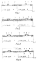
- the polysilicon structures 38 are covered by the resist masks 20 and 26.
- the polysilicon structures 38 do not receive any implants enabling them to serve as, for example, undoped polysilicon resistors of the type often used in static RAM cell loads. Since the polysilicon structures 38 are masked also during the isotropic etching step to remove the sidewall spacers 18 from the gates 12, in the final structure the sidewall spacers 40 remain on the polysilicon structures 38.
Landscapes
- Metal-Oxide And Bipolar Metal-Oxide Semiconductor Integrated Circuits (AREA)
Claims (5)
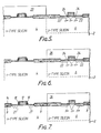
- Procédé de fabrication de transistors MOS à effet de champ à canal p et à canal n complémentaires, le procédé comportant les étapes qui consistent à:(a) réaliser des électrodes de grille (12) pour des transistors MOS à effet de champ (36, 34) à canal p et à canal n complémentaires, chaque électrode de grille (12) étant située sur une couche d'oxyde respective (10) qui s'étend sur une région respective de silicium (4, 6) respectivement dopée par une impureté de type n ou p, les électrodes de grille (12) étant séparées par une région d'oxyde d'isolation (8);(b) former sur les électrodes de grille (12) et les parties exposées adjacentes de la couche d'oxyde (10), une couche d'arrêt isolante (14);(c) former sur la couche d'arrêt isolante (4) une couche (16) pouvant être attaquée; et(d) à attaquer de façon anisotrope la couche (16) pouvant être attaquée pour disposer des espaceurs latéraux (18) de la couche (16) pouvant être attaquée sur la couche d'arrêt isolante (14) et au voisinage des électrodes de grille (12);
dans lequel le transistor MOS à effet de champ (34) à canal n est un transistor MOS à effet de champ (34) à drain légèrement dopé et est réalisé par les étapes (e) à (i) qui consiste à:(e) masquer la région n du silicium (4);(f) implanter une impureté dopante de type n+ dans la région p non masquée du silicium, les espaceurs latéraux (18) situés au-dessus de la région p jouant le rôle de masques empêchant l'implantation dans des parties de la région p (6) qui sont situées sous lesdits espaceurs latéraux (18);(g) attaquer lesdits espaceurs latéraux (18) à partir de la couche d'arrêt isolante (14);(h) implanter une impureté dopante de type n- dans lesdites parties de la région p (6); et(i) retirer le masque de la région n (4) du silicium; et
dans lequel le transistor MOS à effet de champ (36) à canal p est réalisé soit avant soit après le transistor MOS à effet de champ (34) à canal n par les étapes (j) à (1) qui consistent à:(j) masquer la région p (6) du silicium;(k) implanter une impureté dopante de type p+ dans la région n (4) non masquée du silicium, les espaceurs latéraux (18) situés au-dessus de la région n (4) jouant le rôle de masques empêchant l'implantation dans des parties de la région n (4) qui sont situées sous lesdits espaceurs latéraux (18); et(l) retirer le masque de la région p (6) du silicium;
caractérisé en ce que la couche (16) pouvant être attaquée est composée d'un matériau isolant; et
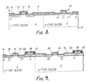
en ce que la réalisation du transistor MOS à effet de champ (36) à canal p comprend l'étape supplémentaire qui consiste à:(m) faire diffuser l'implant de type p+ vers la grille respective (12) afin de produire ainsi un transistor MOS à effet de champ (36) à canal p à chevauchement de drain nul. - Procédé selon la revendication 1, dans lequel le transistor MOS à effet de champ (36) à canal p est réalisé avec un chevauchement de drain nul sans retirer les espaceurs latéraux (18) situés au-dessus de la région n, et dans lequel l'impureté de type p+ implantée est amenée à diffuser vers des emplacements situés sous lesdits espaceurs latéraux (18).
- Procédé selon la revendication 1 ou la revendication 2, comportant en outre l'étape consistant, avant l'étape (b), à déposer sur la région d'oxyde d'isolation (8) une structure (38) permettant de former un élément résistif, et dans lequel, lors de l'étape (b), la couche isolante est formée sur l'oxyde d'isolation (8) et ladite structure (38).
- Procédé selon l'une quelconque des revendications 1 à 3, dans lequel la couche isolante (14) est composée de nitrure de silicium.
- Procédé selon l'une quelconque des revendications 1 à 4, dans lequel la couche (16) pouvant être attaquée est composée d'oxyde de silicium.
Applications Claiming Priority (2)
| Application Number | Priority Date | Filing Date | Title |
|---|---|---|---|
| GB888820058A GB8820058D0 (en) | 1988-08-24 | 1988-08-24 | Mosfet & fabrication method |
| GB8820058 | 1988-08-24 |
Publications (3)
| Publication Number | Publication Date |
|---|---|
| EP0356202A2 EP0356202A2 (fr) | 1990-02-28 |
| EP0356202A3 EP0356202A3 (en) | 1990-10-10 |
| EP0356202B1 true EP0356202B1 (fr) | 1994-11-02 |
Family
ID=10642609
Family Applications (1)
| Application Number | Title | Priority Date | Filing Date |
|---|---|---|---|
| EP89308501A Expired - Lifetime EP0356202B1 (fr) | 1988-08-24 | 1989-08-22 | Transistor à effet de champ MOS et procédé pour sa fabrication |
Country Status (5)
| Country | Link |
|---|---|
| US (1) | US5087582A (fr) |
| EP (1) | EP0356202B1 (fr) |
| JP (1) | JP3270038B2 (fr) |
| DE (1) | DE68919172T2 (fr) |
| GB (1) | GB8820058D0 (fr) |
Families Citing this family (21)
| Publication number | Priority date | Publication date | Assignee | Title |
|---|---|---|---|---|
| US5399514A (en) * | 1990-04-24 | 1995-03-21 | Seiko Epson Corporation | Method for manufacturing improved lightly doped diffusion (LDD) semiconductor device |
| EP0456318B1 (fr) * | 1990-05-11 | 2001-08-22 | Koninklijke Philips Electronics N.V. | Procédé du type CMOS utilisant des espaceurs de nitrure de silicium placés temporairement pour faire des transistors à drains faiblement dopés |
| JP2994128B2 (ja) * | 1991-03-04 | 1999-12-27 | シャープ株式会社 | 半導体装置の製造方法 |
| JP2982383B2 (ja) * | 1991-06-25 | 1999-11-22 | 日本電気株式会社 | Cmosトランジスタの製造方法 |
| US5514616A (en) * | 1991-08-26 | 1996-05-07 | Lsi Logic Corporation | Depositing and densifying glass to planarize layers in semi-conductor devices based on CMOS structures |
| JPH06151828A (ja) * | 1992-10-30 | 1994-05-31 | Toshiba Corp | 半導体装置及びその製造方法 |
| US5468666A (en) * | 1993-04-29 | 1995-11-21 | Texas Instruments Incorporated | Using a change in doping of poly gate to permit placing both high voltage and low voltage transistors on the same chip |
| EP0637073A1 (fr) * | 1993-07-29 | 1995-02-01 | STMicroelectronics S.r.l. | Procédé de réalisation de transistors M.O.S. à canaux P pour dispositifs complémentairs (CMOS) |
| US5416036A (en) * | 1993-10-04 | 1995-05-16 | United Microelectronics Corporation | Method of improvement ESD for LDD process |
| US5786247A (en) | 1994-05-06 | 1998-07-28 | Vlsi Technology, Inc. | Low voltage CMOS process with individually adjustable LDD spacers |
| US5405791A (en) * | 1994-10-04 | 1995-04-11 | Micron Semiconductor, Inc. | Process for fabricating ULSI CMOS circuits using a single polysilicon gate layer and disposable spacers |
| US5661069A (en) * | 1995-06-06 | 1997-08-26 | Lsi Logic Corporation | Method of forming an MOS-type integrated circuit structure with a diode formed in the substrate under a polysilicon gate electrode to conserve space |
| US5714413A (en) * | 1995-12-11 | 1998-02-03 | Intel Corporation | Method of making a transistor having a deposited dual-layer spacer structure |
| US5783470A (en) * | 1995-12-14 | 1998-07-21 | Lsi Logic Corporation | Method of making CMOS dynamic random-access memory structures and the like |
| US5956583A (en) * | 1997-06-30 | 1999-09-21 | Fuller; Robert T. | Method for forming complementary wells and self-aligned trench with a single mask |
| US6221709B1 (en) | 1997-06-30 | 2001-04-24 | Stmicroelectronics, Inc. | Method of fabricating a CMOS integrated circuit device with LDD N-channel transistor and non-LDD P-channel transistor |
| GB2362028B (en) * | 2000-05-04 | 2004-10-20 | Mitel Corp | Method of forming spacers in CMOS devices |
| TW480733B (en) * | 2001-04-10 | 2002-03-21 | Ind Tech Res Inst | Self-aligned lightly doped drain polysilicon thin film transistor |
| US6770921B2 (en) | 2001-08-31 | 2004-08-03 | Micron Technology, Inc. | Sidewall strap for complementary semiconductor structures and method of making same |
| US20150214345A1 (en) * | 2014-01-27 | 2015-07-30 | Globalfoundries Inc. | Dopant diffusion barrier to form isolated source/drains in a semiconductor device |
| US9804046B2 (en) * | 2015-10-27 | 2017-10-31 | DunAn Sensing, LLC | Pressure sensor with support structure for non-silicon diaphragm |
Citations (1)
| Publication number | Priority date | Publication date | Assignee | Title |
|---|---|---|---|---|
| US4209716A (en) * | 1977-05-31 | 1980-06-24 | Texas Instruments Incorporated | Semiconductor integrated circuit with implanted resistor element in second-level polycrystalline silicon layer |
Family Cites Families (9)
| Publication number | Priority date | Publication date | Assignee | Title |
|---|---|---|---|---|
| DE3583472D1 (de) * | 1984-08-28 | 1991-08-22 | Toshiba Kawasaki Kk | Verfahren zum herstellen einer halbleiteranordnung mit gateelektrode. |
| EP0218408A3 (fr) * | 1985-09-25 | 1988-05-25 | Hewlett-Packard Company | Procédé pour fabriquer une structure de drain faible dopée (LLD) dans des circuits intégrés |
| US4843023A (en) * | 1985-09-25 | 1989-06-27 | Hewlett-Packard Company | Process for forming lightly-doped-drain (LDD) without extra masking steps |
| EP0216053A3 (fr) * | 1985-09-26 | 1988-01-20 | Motorola, Inc. | Ecarteur enlevable accolé à une paroi pour la formation à l'aide d'un seul niveau de masquage d'un drain faiblement dopé |
| JPS62190862A (ja) * | 1986-02-18 | 1987-08-21 | Matsushita Electronics Corp | 相補型mos集積回路の製造方法 |
| JPS62290176A (ja) * | 1986-06-09 | 1987-12-17 | Oki Electric Ind Co Ltd | 半導体装置の製造方法 |
| FR2601817B1 (fr) * | 1986-07-18 | 1988-09-16 | Bois Daniel | Procede de fabrication d'un circuit integre comportant un transistor a effet de champ a doubles jonctions et un condensateur |
| US4757026A (en) * | 1986-11-04 | 1988-07-12 | Intel Corporation | Source drain doping technique |
| US4764477A (en) * | 1987-04-06 | 1988-08-16 | Motorola, Inc. | CMOS process flow with small gate geometry LDO N-channel transistors |
-
1988
- 1988-08-24 GB GB888820058A patent/GB8820058D0/en active Pending
-
1989
- 1989-08-21 US US07/396,844 patent/US5087582A/en not_active Expired - Lifetime
- 1989-08-22 DE DE68919172T patent/DE68919172T2/de not_active Expired - Fee Related
- 1989-08-22 EP EP89308501A patent/EP0356202B1/fr not_active Expired - Lifetime
- 1989-08-23 JP JP21716489A patent/JP3270038B2/ja not_active Expired - Fee Related
Patent Citations (1)
| Publication number | Priority date | Publication date | Assignee | Title |
|---|---|---|---|---|
| US4209716A (en) * | 1977-05-31 | 1980-06-24 | Texas Instruments Incorporated | Semiconductor integrated circuit with implanted resistor element in second-level polycrystalline silicon layer |
Also Published As
| Publication number | Publication date |
|---|---|
| JPH02162761A (ja) | 1990-06-22 |
| DE68919172T2 (de) | 1995-04-13 |
| US5087582A (en) | 1992-02-11 |
| EP0356202A3 (en) | 1990-10-10 |
| EP0356202A2 (fr) | 1990-02-28 |
| GB8820058D0 (en) | 1988-09-28 |
| DE68919172D1 (de) | 1994-12-08 |
| JP3270038B2 (ja) | 2002-04-02 |
Similar Documents
| Publication | Publication Date | Title |
|---|---|---|
| EP0356202B1 (fr) | Transistor à effet de champ MOS et procédé pour sa fabrication | |
| US5024959A (en) | CMOS process using doped glass layer | |
| JP3077630B2 (ja) | 半導体装置およびその製造方法 | |
| US5714393A (en) | Diode-connected semiconductor device and method of manufacture | |
| US5406111A (en) | Protection device for an intergrated circuit and method of formation | |
| US5359219A (en) | Silicon on insulator device comprising improved substrate doping | |
| US5880502A (en) | Low and high voltage CMOS devices and process for fabricating same | |
| US5489546A (en) | Method of forming CMOS devices using independent thickness spacers in a split-polysilicon DRAM process | |
| US5674760A (en) | Method of forming isolation regions in a MOS transistor device | |
| US6759717B2 (en) | CMOS integrated circuit device with LDD n-channel transistor and non-LDD p-channel transistor | |
| US20030176033A1 (en) | Disposable spacer technology for reduced cost CMOS processing | |
| US4849364A (en) | Semiconductor devices | |
| JP2003142601A (ja) | 半導体素子のcmos及びその製造方法 | |
| EP0465045B1 (fr) | Procédé pour fabriquer des transistors à effet de champ pour circuits intégrés | |
| US5686324A (en) | Process for forming LDD CMOS using large-tilt-angle ion implantation | |
| US5705439A (en) | Method to make an asymmetrical LDD structure for deep sub-micron MOSFETS | |
| EP0418670B1 (fr) | Procédé pour la fabrication de circuits BiMOS de haute performance | |
| KR100395668B1 (ko) | Cmos집적회로제조방법 | |
| US6583013B1 (en) | Method for forming a mixed voltage circuit having complementary devices | |
| US20010035558A1 (en) | Sacrificial spacer for integrated circuit transistors | |
| US5070029A (en) | Semiconductor process using selective deposition | |
| EP0399231B1 (fr) | Procédé pour la fabrication d'un dispositif à semi-conducteur | |
| US5731240A (en) | Manufacturing method for semiconductor depositing device | |
| JPH06104272A (ja) | 半導体装置及び製造方法 | |
| US7560779B2 (en) | Method for forming a mixed voltage circuit having complementary devices |
Legal Events
| Date | Code | Title | Description |
|---|---|---|---|
| PUAI | Public reference made under article 153(3) epc to a published international application that has entered the european phase |
Free format text: ORIGINAL CODE: 0009012 |
|
| AK | Designated contracting states |
Kind code of ref document: A2 Designated state(s): DE FR GB IT NL |
|
| PUAL | Search report despatched |
Free format text: ORIGINAL CODE: 0009013 |
|
| RHK1 | Main classification (correction) |
Ipc: H01L 21/84 |
|
| AK | Designated contracting states |
Kind code of ref document: A3 Designated state(s): DE FR GB IT NL |
|
| 17P | Request for examination filed |
Effective date: 19901210 |
|
| 17Q | First examination report despatched |
Effective date: 19921023 |
|
| GRAA | (expected) grant |
Free format text: ORIGINAL CODE: 0009210 |
|
| AK | Designated contracting states |
Kind code of ref document: B1 Designated state(s): DE FR GB IT NL |
|
| PG25 | Lapsed in a contracting state [announced via postgrant information from national office to epo] |
Ref country code: NL Effective date: 19941102 |
|
| REF | Corresponds to: |
Ref document number: 68919172 Country of ref document: DE Date of ref document: 19941208 |
|
| ITF | It: translation for a ep patent filed | ||
| ET | Fr: translation filed | ||
| NLV1 | Nl: lapsed or annulled due to failure to fulfill the requirements of art. 29p and 29m of the patents act | ||
| PLBE | No opposition filed within time limit |
Free format text: ORIGINAL CODE: 0009261 |
|
| STAA | Information on the status of an ep patent application or granted ep patent |
Free format text: STATUS: NO OPPOSITION FILED WITHIN TIME LIMIT |
|
| 26N | No opposition filed | ||
| REG | Reference to a national code |
Ref country code: FR Ref legal event code: TP |
|
| REG | Reference to a national code |
Ref country code: GB Ref legal event code: 732E |
|
| REG | Reference to a national code |
Ref country code: FR Ref legal event code: D6 |
|
| PGFP | Annual fee paid to national office [announced via postgrant information from national office to epo] |
Ref country code: FR Payment date: 20000811 Year of fee payment: 12 |
|
| PGFP | Annual fee paid to national office [announced via postgrant information from national office to epo] |
Ref country code: DE Payment date: 20000814 Year of fee payment: 12 |
|
| REG | Reference to a national code |
Ref country code: GB Ref legal event code: IF02 |
|
| PG25 | Lapsed in a contracting state [announced via postgrant information from national office to epo] |
Ref country code: FR Free format text: LAPSE BECAUSE OF NON-PAYMENT OF DUE FEES Effective date: 20020430 |
|
| PG25 | Lapsed in a contracting state [announced via postgrant information from national office to epo] |
Ref country code: DE Free format text: LAPSE BECAUSE OF NON-PAYMENT OF DUE FEES Effective date: 20020501 |
|
| REG | Reference to a national code |
Ref country code: FR Ref legal event code: ST |
|
| PGFP | Annual fee paid to national office [announced via postgrant information from national office to epo] |
Ref country code: GB Payment date: 20020821 Year of fee payment: 14 |
|
| PG25 | Lapsed in a contracting state [announced via postgrant information from national office to epo] |
Ref country code: GB Free format text: LAPSE BECAUSE OF NON-PAYMENT OF DUE FEES Effective date: 20030822 |
|
| GBPC | Gb: european patent ceased through non-payment of renewal fee | ||
| PG25 | Lapsed in a contracting state [announced via postgrant information from national office to epo] |
Ref country code: IT Free format text: LAPSE BECAUSE OF NON-PAYMENT OF DUE FEES;WARNING: LAPSES OF ITALIAN PATENTS WITH EFFECTIVE DATE BEFORE 2007 MAY HAVE OCCURRED AT ANY TIME BEFORE 2007. THE CORRECT EFFECTIVE DATE MAY BE DIFFERENT FROM THE ONE RECORDED. Effective date: 20050822 |