EP0356565A1 - Lecteur transistorisé pour un système de mesure d'opérations cumulatives - Google Patents
Lecteur transistorisé pour un système de mesure d'opérations cumulatives Download PDFInfo
- Publication number
- EP0356565A1 EP0356565A1 EP88114347A EP88114347A EP0356565A1 EP 0356565 A1 EP0356565 A1 EP 0356565A1 EP 88114347 A EP88114347 A EP 88114347A EP 88114347 A EP88114347 A EP 88114347A EP 0356565 A1 EP0356565 A1 EP 0356565A1
- Authority
- EP
- European Patent Office
- Prior art keywords
- signals
- digit
- measurement system
- data
- reader
- Prior art date
- Legal status (The legal status is an assumption and is not a legal conclusion. Google has not performed a legal analysis and makes no representation as to the accuracy of the status listed.)
- Granted
Links
Images


Classifications
-
- G—PHYSICS
- G06—COMPUTING OR CALCULATING; COUNTING
- G06F—ELECTRIC DIGITAL DATA PROCESSING
- G06F11/00—Error detection; Error correction; Monitoring
- G06F11/30—Monitoring
- G06F11/34—Recording or statistical evaluation of computer activity, e.g. of down time, of input/output operation ; Recording or statistical evaluation of user activity, e.g. usability assessment
- G06F11/3409—Recording or statistical evaluation of computer activity, e.g. of down time, of input/output operation ; Recording or statistical evaluation of user activity, e.g. usability assessment for performance assessment
- G06F11/3419—Recording or statistical evaluation of computer activity, e.g. of down time, of input/output operation ; Recording or statistical evaluation of user activity, e.g. usability assessment for performance assessment by assessing time
-
- G—PHYSICS
- G06—COMPUTING OR CALCULATING; COUNTING
- G06F—ELECTRIC DIGITAL DATA PROCESSING
- G06F11/00—Error detection; Error correction; Monitoring
- G06F11/30—Monitoring
- G06F11/34—Recording or statistical evaluation of computer activity, e.g. of down time, of input/output operation ; Recording or statistical evaluation of user activity, e.g. usability assessment
- G06F11/3466—Performance evaluation by tracing or monitoring
- G06F11/3485—Performance evaluation by tracing or monitoring for I/O devices
-
- G—PHYSICS
- G07—CHECKING-DEVICES
- G07C—TIME OR ATTENDANCE REGISTERS; REGISTERING OR INDICATING THE WORKING OF MACHINES; GENERATING RANDOM NUMBERS; VOTING OR LOTTERY APPARATUS; ARRANGEMENTS, SYSTEMS OR APPARATUS FOR CHECKING NOT PROVIDED FOR ELSEWHERE
- G07C3/00—Registering or indicating the condition or the working of machines or other apparatus, other than vehicles
- G07C3/02—Registering or indicating working or idle time only
- G07C3/04—Registering or indicating working or idle time only using counting means or digital clocks
-
- G—PHYSICS
- G06—COMPUTING OR CALCULATING; COUNTING
- G06F—ELECTRIC DIGITAL DATA PROCESSING
- G06F2201/00—Indexing scheme relating to error detection, to error correction, and to monitoring
- G06F2201/86—Event-based monitoring
-
- G—PHYSICS
- G06—COMPUTING OR CALCULATING; COUNTING
- G06F—ELECTRIC DIGITAL DATA PROCESSING
- G06F2201/00—Indexing scheme relating to error detection, to error correction, and to monitoring
- G06F2201/88—Monitoring involving counting
Definitions
- This invention relates to improved cumulative operations measurement systems, and more particularly to a reader device, preferably in solid-state form, for reading out the total operations recorded by such a measurement system for a given piece of apparatus.
- a cumulative operations measurement system is one which is sometimes referred to as "an elapsed time indicator", such an indicator being designed to record the total time that has elapsed in the operation of a given apparatus.
- Another system is one which simply records events such as, for example, the number of times that a particular piece of apparatus has been turned on.
- the present invention provides a reader device that will enable a high degree of accuracy and reliability in the reading of the data involved, and will ensure that there has been no data alteration in the system. Furthermore, it provides a reader device conservatively designed such that thorough checks can be performed to guarantee that there has been no data alteration.
- the present invention also provides a simple, efficient, and cost-effective reader for a measurement system that functions to take or record cumulative operations measurements on machines or apparatus of various types.
- the present invention provides, as part of the reader device, an improved, economical logic layout, whereby a relatively small amount of "chip real estate" is taken up in the logic operations required to produce the desired display of a number being read.
- the invention implements the previously stated features so as to provide a filter arrangement associated with the reader whereby the reading of data can be accomplished by simplified digital electronics.
- a very low data rate can be utilized in the reading of data.
- a rate of 500 Hz is preferably selected for the system.
- the above-stated features are realized in a reader device or apparatus which has its own specialized pulse power source; preferably, that power source is included in a custom chip; that is to say, in an integrated circuit that is specially designed to accomplish the aforenoted objectives, being capable of providing a variety of functions for the reader.
- the primary feature of the present invention resides in the reader device or apparatus for reading the data recorded in a cumulative operations measurement system, the reader comprising a source of pulse power; interconnection means for transmitting such power located at said reader device to a transducer contained in the measurement system; further included are means for first providing power to the reader device then, providing power to the measurement system; means for subsequently acquiring the data from the measurement system and displaying such data, further including means for providing plural checks and for indicating faults in the system.
- a filter arrangement is included, such filter arrangement being comprised of certain elements of the measurement system as well as elements of the reader device.
- the particular design of the filter arrangement stems from the fact that a necessarily high output impedance is present in the measurement system, such impedance being on the order of 100,000 ohms. This high output impedance provides damage protection and insures against incorrect hookups, electrostatic discharge, and like problems.
- the reader device includes appropriately selected filter components, the reading of data from the measurement system can thereby be accomplished by simplified digital electronics, as previously noted. Accordingly, a very low data transmission rate can be selected for the composite system.
- the specific arrangement for accomplishing the above noted functions includes a time base, sequencing, and strobing means; a shift right register and driver means; a digit selector, intensity modulator, and leading-zero blanking means; a segment concentrator means; and a means comprising binary-coded-decimal-to-seven-segment decoder and specialized generator, called a seven dashes generator, for indicating bit errors.
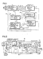
- a main or receiver circuit which is depicted in greater detail in Fig. 2.
- This receiver circuit 10 is provided with a series of connections at its upper side which are labelled PC, DI, R, IP and IC. These individually labelled connections are continued so as to connect with a means 12 for providing time base, sequencing and strobing functions (Fig. 3).
- the labels PC, DI, R, IP and IC stand for power control, data input, reset, interrogation power, and interrogation chopper, respectively, the significance of which will be made apparent hereinafter.
- connection or terminal 12A in the copending application corresponds with connection or terminal 12A in the copending application
- 16 corresponds with connection or terminal 54
- 18 with connection or terminal 59.
- a transducer 20 is depicted as representative of the operations measurement system from which readings are to be taken. Accordingly, the common connection and terminal 14 seen in that figure corresponds with the common bus for the measurement system; the positive power terminal 18 connected to the transducer is an extension of the power bus for the measurement system; and a data input connection 16 seen in Fig. 2 is an extension of the data bus coming from the operations measurement system.
- a pair of terminals X0 and X1 are connected internally, as seen in Fig. 3, to a 32.768 kilohertz oscillator 30. If preferred, an external crystal 32 is connected across the terminals X0 and X1.
- the time base, sequencing and strobing means 12 is additionally connected by the connection 34, seen in Fig. 1, to the means 36, which is designated a binary coded decimal to seven segment decoder and seven dashes generator, and which is illustrated in further detail in Fig. 7.
- Another connection 38 is made from the means 12 to a means designated 40, comprising a digit selector, intensity modulator and leading zero blanking device, illustrated in further detail in Fig. 5.
- connection 42 from means 12 to means 44, the latter comprising a shift register and AB driver, which are illustrated in further detail in Fig. 4.
- a connection 46 extends from the aforenoted shift register and AB driver 44 to the means 40 illustrated in further detail in Fig. 5.
- connection 48 also extending from the means 44 is a connection 48 to a segment concentrator 50 illustrated in further detail in Fig. 6.
- the segment concentrator 50 is connected by connector 52 to the aforenoted means 36.
- connection 54 is also extending from the means 40 to the means 50.
- connection labelled AB involves an output AB from the shift register 44 to the receiver circuit 10.
- a connection, involving a low voltage output designated LV extends from the receiver circuit 10 to the input LV on the means 40.
- another connection is furnished from the means 44 to the means 36 by the output OK (Fig. 4) which, it will be understood, is connected to the identical input designated OK on the means 36 (Fig. 7).
- this receiver circuit 10 is especially designed to provide “single cycle” operation. As will be explained hereinafter, “continuous” operation is also feasible.
- one of the transducers A s or B s is powered by an application-specific integrated circuit known as SK 1561 IC.
- This integrated circuit integrates within one chip all of the means 12, 36, 40, 44, and 50 already described in general functional terms.
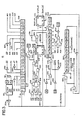
- the DC supply source is as illustrated in Fig.
- This unregulated source 60 is connected to a reverse protection diode 62, and to a network, including a switch 66 in series with resistors 68 and 70; as well as a parallel combination of resistors 72, 74 in series with an NPN transistor 76. Further, a transistor 78 has its input in shunt with resistor 72. An output connection 80 extends down from the collector of transistor 78 to the plus input of an operational amplifier serving as a comparator 82; this arrangement permits a determination of whether an undesirably low voltage has appeared at the output of transistor 78.
- an output R Connected to the top of resistor 68 in the network, by way of resistor 84, is an output R. Additionally, an input PC located immediately below the output R is connected by way of the resistor 86 to the network; specifically to the base of transistor 76. It will be understood that these input or output terminals R and PC correspond with those seen connected in Fig. 1 between the time base circuit and the receiver circuit therein.
- switch 66 In operation, momentary closure of switch 66 causes a reset signal to be applied to initialize the integrated circuit known as SK1561IC. What this means is that the sequence controlled by means 12 will not start until this closure is released, that is, the switch 66 is released. Subsequent closures will restart the sequence regardless of the sequence's status. This feature is particularly useful for quick reacquisition if a fault is identified.
- a signal appears at the input PC in Fig. 2 (from the time base circuit of Fig. 3) to maintain sufficient input current to the NPN-PNP power switch pair for continued operation.
- This pair includes the transistors previously identified as 76 and 78.
- the output voltage at the collector of transistor 78 is reduced by a five-terminal series regulator 90 to 5.50v DC with an approximate 2% tolerance.
- a resistor 104 and resistor 106 are connected to the output of the voltage regulator 90 and program the 5.50v DC.
- the output drivers 194 and 195 therein having outputs designated IC and IP in that figure, become active and produce a relatively fast rising and falling voltage-doubled 9.5 volt pulse for activating either an A S or B S transducer within the transducer block 20.
- a network 92 is seen in Fig. 2 connected to the terminals IP and IC (interrogation power and interrogation chopper respectively), and it includes the diodes 94, 96, and capacitors 98, 102. Further connected between the diode 96 and the terminal 18 of transducer 20 is a short circuit protection resistor 100.
- the data input side of the reader device which includes the data input terminal 16 and the common terminal 14, these are connected to a network 108, which constitutes the "mating" part of the filter arrangement of the present invention.
- the other part of that arrangement is constituted by the necessarily high output impedance already noted (approximately 100,000 ohms) of the measurement system.
- the network 108 includes oppositely shunt-connected diodes 110 and 112, capacitor 114, and resistor 116, the connection from terminal 16 being made by way of resistor 118 (having a value of 10K).
- This resistor 118 effectively then serves as a continuation of the measurement system output impedance.
- the upper end of the network 108 is connected to the plus side of an operational amplifier 120, the negative terminal of which is connected to the junction point of a voltage divider comprising resistors 122 and 124 for establishing the threshold voltage.
- This amplifier 120 thus develops the DI input for the reader device acting as a buffer and threshold voltage detector in processing data signals from the high impedance source provided by the measurement system. Accordingly, a relatively low rate of data transmission from the transducer 20 is established.
- the threshold voltage is nominally 300 millivolts.
- the input resistor 118 and the back-to-back diodes 110 and 112 provide protection in the event of a system fault, diode 110 being for reverse protection.
- the comparator 120 has its reference level adjusted approximately half way up to the clamp level of diode 112. The complete arrangement permits transmission along hundreds of feet of twisted-pair cable, while maintaining extreme fault protection for both the transducer and the reader device.
- the negative terminal of the other comparator 82 is likewise connected to the junction point of the voltage divider comprising resistors 122 and 124; furthermore that suitable input resistors 130 and 132 are connected to the plus terminal of comparator 82.
- the comparator 82 which develops the LV input, senses, as noted before, the unregulated system voltage immediately after the PNP transistor 78 of the power switch. If this voltage drops below 6.3 volts, a signal is sent to the means 40 (Fig. 5) and a suitable "dimming display" is created at the output of this means.
- each of the drivers DA-DG transmits an energizing signal to a respective LED (not shown) in an intensity modulated manner. The dimming is achieved by time modulation. Due to receipt of signal A13 from counter A, 4 Hz alternation from full brightness to half brightness is accomplished.
- Identification of the transducer 20 as being either class A or class B is accomplished from the data transmitted from the operations measurement system, that is, from the transducer 20. This will be explained in some detail hereinafter; but with reference to Figs. 2 and 4, the required information is presented at the AB output of the means 44 in Fig. 4; that is to say, the shift register and AB driver arrangement. As explained previously, connection is made from the AB output of the means 44 to the AB input, seen at the far right in Fig. 2, at which connection is made to a node 129. Identification of transducer A is made by means of a light emitting diode 131 and its accompanying resistor 133, whereas identification of transducer B is accomplished by means of the light emitting diode 135 and its accompanying resistor 137.
- a suitable voltage level is applied at the AB input in Fig. 2 such that, in the case of transducer A, the LED 131 is energized. This is because the voltage level at AB is then sufficiently high to produce this result, whereas, in the case of the identification of transducer B, the voltage level at AB is sufficiently low such that there is a sufficient potential difference between B+ and that voltage level to produce energization of LED 135.
- identification of transducer B what is indicated is that the transducer is one which is counting the number of events; hence a decimal point is not needed whereas in the case of identification of transducer A it means that a decimal point is required to indicate the number of elapsed hours.
- the LED display 490 is activated approximately six seconds after initialization and remains active for fifteen seconds. What this means is that the individual digit drivers, already indicated, that is drivers DA-DG in the means 40, as well as the series of segment drivers SG, SF, SE, SD, SC, SB, SA, and ST, seen in Fig. 7 as part of the means 36, are activated at these predetermined times.
- the logic gates in Fig. 3 are designated by the following even numbers: 150-182; regular and inverting amplifiers by the even numbers 184-206; Schmitt triggers by the even numbers 208-212; flip-flops by the even numbers 214 and 216; and counters A, B, C, and D by the even numbers 218-224.
- the basic machine cycle is 64 seconds in duration.
- the first cycle after the reset (R) initialization already described, differs from all subsequent cycles in that the display is blanked until the first data search is complete. Thereafter, the display remains active, except for short blanking intervals during data refresh.
- the first machine cycle is illustrated in the timing diagram shown in Figs. 8 and 9. Subsequent cycles will be identical to that shown in Fig. 9 except that "DISPLAY" remains at a logic 1. Also, PC goes to a logic 1 at the beginning of reset (R) during the first cycle, and also on the falling edge of A20 on subsequent cycles.
- the 32.768 kilohertz oscillator 30 seen in Fig. 3 is controlled, as already noted, by the external crystal 32, being designed for Pierce (or parallel) operation. This crystal is shown as the only external component, as the phase shift capacitors and amplifier may be integrated within the integrated circuit.
- the oscillator 30 starts within one second after power is applied (see Fig. 8 - where the delay is shown exaggerated).
- the counter 218, or A counter is a ripple binary counter and advances on falling edges only.
- the outputs IC and IP outputs symbolizing interrogation chopper and interrogation power respectively) are derived exclusively from the A counter and therefore change state on falling clock edges.
- the outputs of the A counter that are particularly involved are A2, A15, A16, A16 , A17, A17 , A18, A19, and A20.
- IP is normally at logic 0, and goes to logic 1 for precisely three seconds; whereas IC is normally at logic 0 and then oscillates between logic 0 and logic 1 at an 8.196 kilohertz rate whenever IP is active.
- flip-flop 214 the Q output thereof labelled “SEARCH” sets and resets on a rising clock edge (see Fig. 8), one half clock cycle after the data input to the flip-flop 214 changes.
- the output RC is a necessary "first” reset and is a redundant reset during continuous operation.
- "SEARCH” is normally at logic 0 and goes to a logic 1 for precisely 1.5 seconds.
- RS seen at the output of trigger 210, is a once, and only once, initial reset. RS is asynchronous and is in phase and "squared up” (because of the Schmitt trigger 210) with respect to the input R (seen at the input of the trigger 210).
- RC equals RS whenever A21 is a logic 0 because of the OR gate 170. RC is therefore asynchronous during startup and synchronous during continuous operation. It will also be understood that the " DATA" and “DATA” outputs are the in-phase and out-of-phase "squared up” versions of the input labelled DI (just below the input R). These outputs are both asynchronous.
- the counter 220 advances on the falling edge of A7 (Fig. 10) during "SEARCH” (input of logic gate 168), provided that the reset R of counter 220 has been released by RC and DATA (inputs of logic gate 172). It therefore advances on a falling edge of the clock. If “ DATA " remains at a logic 0 until the B counter reaches a state of 0000001, the B counter's clock loop will lock up, having counted 61 cycles on A7 alternations (238.28 milliseconds). The B counter will normally be reset when DATA returns to logic 1 and is, therefore, prepared to repeat the count-out cycle. When B7 returns to logic 0, the B counter will advance one count. If it counts 61 cycles of A7 alternations for a second time (during the search interval), it will be armed and ready to advance the C counter, or counter 222, a second time.
- the above-described operation constitutes a "rough frequency check".
- the half cycle is at least 238 milliseconds long.
- two cycles have to occur during the search operation to "arm" the acquisition sequence.
- the degree of resolution in performing the frequency check can be as fine or precise as desired.
- the counter 222 or C counter has two stages, C1 and C2, and C2 completes its final transition to a logic 1 on an asynchronous falling edge (reset by "DATA" is asynchronous). Subsequently, this enables falling edge clock counting by the D counter, also designated 224. After 32 counts of the clock (976.56 microseconds), the first strobe (D6 rising edge) is generated. Subsequent strobes are spaced 1.953 milliseconds apart. After 32 strobes are generated, the loop will lock up, as D12, the last stage of the D counter, will go to a logic 1 on the falling edge of the thirty-second strobe. The interval during which the strobe generator is functional is defined as “LOAD” and " LOAD ".
- the power control signal PC which is developed by the logic effected by the combination of logic gates 174, 176, 178 and the invertor 202, is generated directly from the A counter, as will be apparent from Fig. 3.
- This power control signal may contain switching transients, which are permissible.
- the elements forming means 44 are seen in schematic form, such means comprising a shift register 250 and an AB driver 252. Additionally included is an OK driver 254.
- the shift register 250 is 32 bits long and, when loaded by way of the data input seen at the top of the figure, contains twenty eight BCD (binary coded decimal) bits, an AB bit, and three check bits (E1, E31, and E32. As has been noted previously, these check bits allow for checking on various functions and operations of the system. Shift register 250 is reset once, and only once, during startup by dint of the RS input, also seen at the top of Fig. 4. This RS input is only used for testing, as each loading sequence essentially clears the register by pushing in "new" data. "DATA" is shifted each time the input at D6 (strobe or enable) presents a rising edge at the clock input.
- AB driver circuit 252 includes logic gates 264, 266, 268, as well as inverter 270 and amplifier 272.
- bit E1 should be logic
- bit E32 should be logic 1
- bit E31 should be the inverse of bit E2.
- bit E3-E30 contain the binary coded decimal data.
- the first binary coded decimal includes bits E3, E4, E5, and E6, whose output lines are designated 1A, 2A, 4A, and 8A in Fig. 4.
- the OK output of the means 44 illustrated in Fig. 4 is connected to the OK input of the means 36 depicted in Fig. 7, specifically to the input of logic gate 436; whereas the output AB, as noted previously, connects to the AB input or terminal of Fig. 2.
- the AB output serves two functions. First, it signals the presence of data during the initial 5 seconds of the first machine cycle. Second, it shows the status of the E2 bit after the display is enabled ("DISPLAY" becomes a logic 1 at 5 seconds and remains there until power is removed, or is externally reset via "R”). During the first five seconds, AB will be logic 1 whenever " DATA " is logic 1, and logic 0 whenever " DATA " is logic 0. After the first five seconds, AB will be logic 1 whenever E2 is logic 1, whereas AB will be logic 0 whenever E2 is logic 0.
- the output " E2 " in Fig. 4 is connected to an input of logic gate 458 of means 36 in Fig. 7 for decimal point display purposes.
- Fig. 5 there is depicted the means 40 which includes an arrangement for digit selection, intensity modulation, and leading-zero blanking.
- Logic gates having conventional symbols are designated by the following even numbers: 300-346; inverters are designated 348 and 350.
- Digit selection is derived directly from the A counter, the particular inputs for this purpose being A5, A5 , A6, A6 , A7, A7 .
- Fig. 10 summarizes the selection sequence.
- the logic imposed by the gates 310-316 in Fig. 5 on the signals A5, A5 , A6, A6 , and the further logic imposed by the gates 320-332 on the resultant signals therefrom, as well as on the logic signals A7 and A7 yields outputs at the latter gates which are designated A m -G m (modulation signals).
- the sequential pulse patterns of these modulation signals A m -G m can be appreciated from Fig. 10.
- the signals A m -G m are also transmitted to the means 50 in Fig. 6, the purposes of which will be explained hereinafter.
- Fig. 10 shows the effect on a typical digit driver DG.
- the segment concentrator 50 consists of four channels of seven line to one line time division selection.
- the first group comprising NAND gates 360-372, all having their outputs tied to the inputs of NAND gate 374 whose output is designated 1H.
- the second group of logic NAND gates is evenly numbered 376-388, all of whose outputs are connected to the inputs of NAND gate 390 whose output is designated 2H.
- a third group is numbered 392-404, all of whose outputs are connected to NAND logic gate 406, whose output is designated 4H.
- a fourth group is numbered 408-420, all of whose outputs are connected to NAND logic gate 422 whose output is designated 8H.
- the seven binary coded digits being processed are concentrated by the means 50 into a single time sequence digit in order to reduce the BCD-to-seven segment decoding to a single entity.
- This concentration is accomplished by applying to the inputs of the logic gates in Fig. 6 particular time-division signals from the respective outputs of the logic gates 320-332 in Fig. 5.
- the G m signal which is representative of the most significant decimal digit, is applied to inputs of logic gates 360, 376, 392, and 408.
- binary coded signals representative of the most significant decimal digit are being transmitted from bit locations E27-E30 in Fig.
- the other modulation or time-division signals A m -F m are similarly transmitted and then similarly produce the resultant signals 1H, 2H, 4H, and 8H shown in Fig. 6.
- the means 36 include the even numbered logic gates 430-474; the inverters 476-482; and the flip-flops 484, 486, and 488.
- P channel devices Connected to the outputs of the respective gates 458-472 are P channel devices, which are the segment drivers SP, SA, SB, SC, SD, SE, SF, and SG.
- the uppermost of these, that is, driver SP takes care of the decimal point which, as noted before, is required when the reader is receiving information about cumulative numbers of hours, that is, from an events counter.
- the decimal point P (seen in Fig. 11) is assigned a time slot allocated for the "DC" digit driver (Fig. 5) in order to uniquely access that point in a dedicated 8 segment by seven digit (15 line) LED array, as for example shown in Fig. 13. It will be understood that the decimal point is enabled when E2 is a logic 0.
- the outputs from the segment concentrator 50 (Fig. 6); that is to say, the outputs 1H, 2H, 4H, and 8H, are continuously decoded from BCD into the 7 segment format by the gate array, which includes logic gates 440-454 in Fig. 7.
- the gate array which includes logic gates 440-454 in Fig. 7.
- output line marked 7D (immediately above the segment driver SP), is connected back to the means 40 in Fig. 5; that is, it is connected to the uppermost input labelled 7D in that figure.
- this "7 dashes generator” signifies that an error has occurred and it takes precedence over digit data.
- Output line 7D also connects to all the NOR gates 458-470 in Fig. 7, causing the outputs at each to become a logic 1, except at NOR gate 472 which becomes a logic 0.
- segment drivers SP-SF go OFF because each respective P channel device is OFF.
- segment driver SG is ON because of the output state at NOR gate 472.
- the first condition is an illegal BCD number, and it is flagged by the "bit fail" flip-flop, that is to say, flip-flop 488.
- the second condition is an illegal logic statement in locations E1, E31, or E32 of shift register 250, which is also flagged by the flip-flop 488.
- the third condition is the inability to find two acceptable data groups within the search interval, and it is flagged by the "no find" flip-flop, that is, flip-flop 486.
- the "bit fail" flip-flop 488 is set on the rising edge of a clock if the data input is logic 1.
- the logic 1 can signify that the 8H bit is present simultaneously with the 4H bit and/or a 2H bit.
- the 2H, 4H, and 8H bits change their states in response to the A counter and therefore, change on the falling edge of a clock pulse.
- a logic 1 can also signify that there is an illegal logic state in at least one of the shift register locations E1, E31, or E32.
- the flip-flop 488 is initially held reset by the presence of the DISPLAY at the input of OR gate 438. This flip-flop is subsequently reset each time new data is shifted into shift register 250 (during "LOAD").
- the first failure causes flip-flop 488 to lock up via the feedback from Q . It can only be released via a reset.
- the "no find” flip-flop that is, flip-flop 486, will produce a logic 0 at its Q output if a valid "LOAD” signal had not been developed during the "SEARCH” interval.
- the "LOAD” memory LM flip-flop or flip-flop 484) will either remain reset or be set by "LOAD” if the "SEARCH” was successful.
- Fig. 5 of the copending application is a timing diagram depicting a preferred format in which the readout data is presented by the serial encoder 50 and the output buffer 52 in the measurement system to the reader (Fig. 4) in that same application.
- transducer 20 symbolizes that serial encoder and output buffer.
- the recorded data is read out such that a serial stream of data appears at the terminals 14 and 16 in Fig. 2 of this application.
- Each data readout cycle begins with a positive-going signal voltage front indicating constant logic 1 up to a predetermined point in time, at which point the voltage drops to a logic 0 level.
- the data presented at the terminals 14 and 16 in Fig. 2 herein is indicated by the presence or absence of logic 1 signals over a series of intervals numbered 1-32, which correspond to the bit positions or locations E1-E32 in Fig. 4 of this application.
- the bit positions E1, E2, E31, and E32 are for special purposes: namely, E1, E31, and E32 are for checking purposes to ensure that certain criteria have been met; whereas E2 is indicative of which type transducer is involved in the measurement system, which determines whether or not a decimal point is to appear in the display.
- the data stored in the measurement system has a decimal value of 7654329.
- This data in binary-coded decimal form will be transmitted in accordance with the low data rate of 500 Hz, and will be amplified and processed by amplifier 120, which has the output DI.
- a serial stream of BCD data appears at the output DI of amplifier 120 (Fig. 2), which is connected to the input designated DI in Fig. 3.
- This stream of data is then entered into shift register 250 (Fig. 4) by dint of the DATA, RS and D6 (strobe or enable) inputs already noted.
- the binary-coded values representative of the exemplary decimal value 7654329 being transmitted are seen immediately to the left of respective bit locations E3-E30 of shift register 250 in Fig. 4.
- the decimal digit 7 which appears as the most significant digit in Fig. 4 is transmitted in binary coded form on the output lines 1G, 2G, 4G, and 8G to the segment concentrator 50 of Fig. 6.
- a binary value of "1" appears at the input 1G of the logic gate 360 in Fig. 6; whereas a binary value of 1 also appears at the input 2G of logic gate 376; and, a binary value of 1 at the input 4G of the logic gate 392; however, a binary value 0 appears at the input 8G of logic gate 408.
- the time-divisional multiplex signal G m also appears at another input of those same respective logic gates for reasons already given (see Fig. 12), the binary coded signals at the outputs 1H, 2H, 4H, and 8H in Fig. 6, and hence at the corresponding inputs in Fig. 7, have values respectively of 1110.
- the appearance of these signals produces at the segment drivers SA-SG in Fig. 7 the pulse patterns seen in Fig. 12. Consequently, as seen at the bottom of Fig. 12, the suitable decoding that takes place in the decoder of Fig. 7 yields a combination of segment illuminations ABC which define the decimal digit 7 which is to be displayed at the particular digit display location representing the most significant digit.
- the preferred embodiment has been referenced to single-cycle operation, and, in that context, the receiver circuit is as depicted in Fig. 2.
- the transducer is powered independently of the SK1561 integrated circuit, although preferably from the same power bus.
- the alternate circuit embodiment depicted in Fig. 13 governs the operation.
- the clock is shown emanating from the transducer.
- the resistor-capacitor-diode network is for "power on" reset, but may be eliminated (by connecting R to common) if the integrity of the data is unimportant during the first sixty seconds or so of operation.
- the "power on" reset guarantees that valid data will appear within six seconds, and that the display will remain blanked until valid data is received.
- the AB, PC, IP, and IC outputs are not connected (N/C).
- the display 500 in Fig. 13 is a seven digit, seven segment, plus decimal point (if required), light emitting diode array.
- the display is updated at 64 second intervals and is blanked for 64 milliseconds whenever "new" data is acquired.
- Resistors 502 set the LED current.
Landscapes
- Engineering & Computer Science (AREA)
- General Engineering & Computer Science (AREA)
- Theoretical Computer Science (AREA)
- Physics & Mathematics (AREA)
- General Physics & Mathematics (AREA)
- Computer Hardware Design (AREA)
- Quality & Reliability (AREA)
- Arrangements For Transmission Of Measured Signals (AREA)
Priority Applications (1)
| Application Number | Priority Date | Filing Date | Title |
|---|---|---|---|
| DE19883852392 DE3852392T2 (de) | 1988-09-02 | 1988-09-02 | Solid-state-Lesevorrichtung für ein kumulatives Betriebsmesssystem. |
Applications Claiming Priority (1)
| Application Number | Priority Date | Filing Date | Title |
|---|---|---|---|
| US07/071,801 US4852104A (en) | 1987-07-10 | 1987-07-10 | Solid-state reader device for a cumulative operations measurement system |
Publications (2)
| Publication Number | Publication Date |
|---|---|
| EP0356565A1 true EP0356565A1 (fr) | 1990-03-07 |
| EP0356565B1 EP0356565B1 (fr) | 1994-12-07 |
Family
ID=22103677
Family Applications (1)
| Application Number | Title | Priority Date | Filing Date |
|---|---|---|---|
| EP88114347A Expired - Lifetime EP0356565B1 (fr) | 1987-07-10 | 1988-09-02 | Lecteur transistorisé pour un système de mesure d'opérations cumulatives |
Country Status (2)
| Country | Link |
|---|---|
| US (1) | US4852104A (fr) |
| EP (1) | EP0356565B1 (fr) |
Cited By (3)
| Publication number | Priority date | Publication date | Assignee | Title |
|---|---|---|---|---|
| EP0478461A1 (fr) * | 1990-09-28 | 1992-04-01 | ETAT FRANCAIS représenté par le Délégué Général pour l'Armement | Procédé et dispositif électronique de surveillance et d'archivages d'informations concernant les ensembles et sous-ensembles électroniques, électriques, mécaniques |
| EP1077432A1 (fr) * | 1999-08-18 | 2001-02-21 | Arnaud Caron | Dispositif pour déterminer l'état de vieillissement des toiles et tissus utilisés dans les sports nautiques et aéronautiques et parapente associé |
| EP1041516A3 (fr) * | 1999-03-30 | 2004-05-12 | Oxley Developments Company Limited | Indicateur de données |
Families Citing this family (6)
| Publication number | Priority date | Publication date | Assignee | Title |
|---|---|---|---|---|
| JPH0792630B2 (ja) * | 1988-01-11 | 1995-10-09 | インターナショナル・ビジネス・マシーンズ・コーポレーション | 事務機器 |
| US5202682A (en) * | 1989-07-13 | 1993-04-13 | Curtis Instruments, Inc. | Data encodement and reading method and apparatus |
| EP0804778B1 (fr) * | 1994-12-16 | 1999-07-21 | Vu-Data Limited | Dispositif enregistreur, dispositif de lecture et dispositif de regulation |
| US5698965A (en) * | 1995-12-01 | 1997-12-16 | Flight Systems, Inc. | Apparatus and method for determining the current state of charge of a battery by monitoring battery voltage increases above and decreases below a threshold |
| US5659845A (en) * | 1996-05-30 | 1997-08-19 | Xerox Corporation | Accounting system for use with document processing system |
| CN101320490A (zh) * | 2007-06-07 | 2008-12-10 | 鸿富锦精密工业(深圳)有限公司 | 连接器使用状态监测装置 |
Citations (7)
| Publication number | Priority date | Publication date | Assignee | Title |
|---|---|---|---|---|
| DE2359067A1 (de) * | 1973-03-08 | 1974-09-19 | Robert W Brandt | Verfahren und vorrichtung zur messung der auftrittshaeufigkeit von ereignissen |
| US3934123A (en) * | 1974-02-11 | 1976-01-20 | Viable Systems, Inc. | Event recorder with coded removable display |
| FR2323189A1 (fr) * | 1975-09-04 | 1977-04-01 | Sangamo Weston | Appareil enregistreur de donnees |
| GB2030702A (en) * | 1978-09-29 | 1980-04-10 | Nissan Motor | Mavigation instrument |
| EP0094800A2 (fr) * | 1982-05-14 | 1983-11-23 | Production Control Information (Pci) Limited | Système de commande de production, en particulier pour la fabrication de vêtements |
| DE3233833A1 (de) * | 1982-09-11 | 1984-03-15 | SWF-Spezialfabrik für Autozubehör Gustav Rau GmbH, 7120 Bietigheim-Bissingen | Rechnersystem, insbesondere bordrechner fuer kraftfahrzeuge |
| EP0136043A2 (fr) * | 1983-08-19 | 1985-04-03 | Citizen Watch Co. Ltd. | Appareil pour déterminer la valeur des efforts physiques |
Family Cites Families (5)
| Publication number | Priority date | Publication date | Assignee | Title |
|---|---|---|---|---|
| US3939333A (en) * | 1974-08-09 | 1976-02-17 | Electronic Engineering Co. Of California | Previous events memory |
| US4112926A (en) * | 1976-12-08 | 1978-09-12 | The Children's Memorial Hospital | Method and apparatus for measuring and treating hyperactivity in human beings |
| US4366373A (en) * | 1980-10-14 | 1982-12-28 | Electro Corporation | Event rate counter |
| US4547891A (en) * | 1983-12-08 | 1985-10-15 | Gte Products Corporation | Apparatus for monitoring the performance of a press or like machine |
| US4712195A (en) * | 1986-05-09 | 1987-12-08 | Curtis Instruments, Inc. | Solid-state cumulative operations measurement system |
-
1987
- 1987-07-10 US US07/071,801 patent/US4852104A/en not_active Expired - Fee Related
-
1988
- 1988-09-02 EP EP88114347A patent/EP0356565B1/fr not_active Expired - Lifetime
Patent Citations (7)
| Publication number | Priority date | Publication date | Assignee | Title |
|---|---|---|---|---|
| DE2359067A1 (de) * | 1973-03-08 | 1974-09-19 | Robert W Brandt | Verfahren und vorrichtung zur messung der auftrittshaeufigkeit von ereignissen |
| US3934123A (en) * | 1974-02-11 | 1976-01-20 | Viable Systems, Inc. | Event recorder with coded removable display |
| FR2323189A1 (fr) * | 1975-09-04 | 1977-04-01 | Sangamo Weston | Appareil enregistreur de donnees |
| GB2030702A (en) * | 1978-09-29 | 1980-04-10 | Nissan Motor | Mavigation instrument |
| EP0094800A2 (fr) * | 1982-05-14 | 1983-11-23 | Production Control Information (Pci) Limited | Système de commande de production, en particulier pour la fabrication de vêtements |
| DE3233833A1 (de) * | 1982-09-11 | 1984-03-15 | SWF-Spezialfabrik für Autozubehör Gustav Rau GmbH, 7120 Bietigheim-Bissingen | Rechnersystem, insbesondere bordrechner fuer kraftfahrzeuge |
| EP0136043A2 (fr) * | 1983-08-19 | 1985-04-03 | Citizen Watch Co. Ltd. | Appareil pour déterminer la valeur des efforts physiques |
Cited By (5)
| Publication number | Priority date | Publication date | Assignee | Title |
|---|---|---|---|---|
| EP0478461A1 (fr) * | 1990-09-28 | 1992-04-01 | ETAT FRANCAIS représenté par le Délégué Général pour l'Armement | Procédé et dispositif électronique de surveillance et d'archivages d'informations concernant les ensembles et sous-ensembles électroniques, électriques, mécaniques |
| FR2667413A1 (fr) * | 1990-09-28 | 1992-04-03 | France Etat Armement | Procede et dispositif electronique de surveillance et d'archivage d'informations concernant les ensembles et sous-ensembles electroniques, electriques, mecaniques. |
| EP1041516A3 (fr) * | 1999-03-30 | 2004-05-12 | Oxley Developments Company Limited | Indicateur de données |
| EP1077432A1 (fr) * | 1999-08-18 | 2001-02-21 | Arnaud Caron | Dispositif pour déterminer l'état de vieillissement des toiles et tissus utilisés dans les sports nautiques et aéronautiques et parapente associé |
| FR2797701A1 (fr) * | 1999-08-18 | 2001-02-23 | Arnaud Caron | Dispositif pour determiner l'etat de vieillissement des tissus et des toiles utilises dans la structure des aeronefs legers |
Also Published As
| Publication number | Publication date |
|---|---|
| US4852104A (en) | 1989-07-25 |
| EP0356565B1 (fr) | 1994-12-07 |
Similar Documents
| Publication | Publication Date | Title |
|---|---|---|
| US4093946A (en) | Two-wire, multiple-transducer communications system | |
| US4206449A (en) | Multiple sensor intrusion alarm system | |
| US4852104A (en) | Solid-state reader device for a cumulative operations measurement system | |
| US3987278A (en) | Moving object identifying system | |
| US4228422A (en) | System for displaying at a remote station data generated at a central station and for powering the remote station from the central station | |
| US3936745A (en) | Method of measuring the duration of a discontinuous signal | |
| US5223742A (en) | Circuit and method for monitoring a pulse width modulated waveform | |
| US4290128A (en) | Time sequence monitor | |
| US4528650A (en) | Streamer cable multiplexing apparatus | |
| US4618965A (en) | Monitoring of data transfer system having serially distributed data ports | |
| SU1383361A1 (ru) | Устройство дл контрол логического блока | |
| SU1387044A1 (ru) | Устройство дл контрол блоков посто нной пам ти | |
| EP0186740A1 (fr) | Système de détection de la fréquence du secteur | |
| SU830477A1 (ru) | Преобразователь угла поворотаВАлА B КОд | |
| SU1297060A1 (ru) | Устройство дл контрол логических схем | |
| EP0112948A1 (fr) | Système de détection de la fréquence du secteur | |
| SU1290376A1 (ru) | Устройство дл считывани информации | |
| SU997253A1 (ru) | @ -Триггер с автономной проверкой работоспособности | |
| SU1183970A1 (ru) | Сигнатурный анализатор | |
| SU1275445A1 (ru) | Устройство дл контрол мультиплексора | |
| EP0125011A1 (fr) | Système d'alarme contre le vol avec effraction | |
| SU1267422A1 (ru) | Устройство дл контрол цифровых блоков | |
| SU1181118A1 (ru) | Устройство диагностики неисправностей генератора импульсов | |
| SU1132291A1 (ru) | Устройство дл регистрации сигналов неисправности | |
| SU1376086A1 (ru) | Устройство дл встроенного контрол дешифратора |
Legal Events
| Date | Code | Title | Description |
|---|---|---|---|
| PUAI | Public reference made under article 153(3) epc to a published international application that has entered the european phase |
Free format text: ORIGINAL CODE: 0009012 |
|
| AK | Designated contracting states |
Kind code of ref document: A1 Designated state(s): DE FR GB IT NL |
|
| 17P | Request for examination filed |
Effective date: 19900831 |
|
| 17Q | First examination report despatched |
Effective date: 19920914 |
|
| GRAA | (expected) grant |
Free format text: ORIGINAL CODE: 0009210 |
|
| AK | Designated contracting states |
Kind code of ref document: B1 Designated state(s): DE FR GB IT NL |
|
| PG25 | Lapsed in a contracting state [announced via postgrant information from national office to epo] |
Ref country code: IT Free format text: LAPSE BECAUSE OF FAILURE TO SUBMIT A TRANSLATION OF THE DESCRIPTION OR TO PAY THE FEE WITHIN THE PRE;WARNING: LAPSES OF ITALIAN PATENTS WITH EFFECTIVE DATE BEFORE 2007 MAY HAVE OCCURRED AT ANY TIME BEFORE 2007. THE CORRECT EFFECTIVE DATE MAY BE DIFFERENT FROM THE ONE RECORDED.SCRIBED TIME-LIMIT Effective date: 19941207 Ref country code: FR Effective date: 19941207 Ref country code: NL Effective date: 19941207 |
|
| REF | Corresponds to: |
Ref document number: 3852392 Country of ref document: DE Date of ref document: 19950119 |
|
| EN | Fr: translation not filed | ||
| NLV1 | Nl: lapsed or annulled due to failure to fulfill the requirements of art. 29p and 29m of the patents act | ||
| PLBE | No opposition filed within time limit |
Free format text: ORIGINAL CODE: 0009261 |
|
| STAA | Information on the status of an ep patent application or granted ep patent |
Free format text: STATUS: NO OPPOSITION FILED WITHIN TIME LIMIT |
|
| 26N | No opposition filed | ||
| PGFP | Annual fee paid to national office [announced via postgrant information from national office to epo] |
Ref country code: GB Payment date: 19990826 Year of fee payment: 12 |
|
| PGFP | Annual fee paid to national office [announced via postgrant information from national office to epo] |
Ref country code: DE Payment date: 19990928 Year of fee payment: 12 |
|
| PG25 | Lapsed in a contracting state [announced via postgrant information from national office to epo] |
Ref country code: GB Free format text: LAPSE BECAUSE OF NON-PAYMENT OF DUE FEES Effective date: 20000902 |
|
| GBPC | Gb: european patent ceased through non-payment of renewal fee |
Effective date: 20000902 |
|
| PG25 | Lapsed in a contracting state [announced via postgrant information from national office to epo] |
Ref country code: DE Free format text: LAPSE BECAUSE OF NON-PAYMENT OF DUE FEES Effective date: 20010601 |