EP0356610A2 - Computerterminal - Google Patents
Computerterminal Download PDFInfo
- Publication number
- EP0356610A2 EP0356610A2 EP89104085A EP89104085A EP0356610A2 EP 0356610 A2 EP0356610 A2 EP 0356610A2 EP 89104085 A EP89104085 A EP 89104085A EP 89104085 A EP89104085 A EP 89104085A EP 0356610 A2 EP0356610 A2 EP 0356610A2
- Authority
- EP
- European Patent Office
- Prior art keywords
- slave processor
- computer terminal
- display
- crt
- memory
- Prior art date
- Legal status (The legal status is an assumption and is not a legal conclusion. Google has not performed a legal analysis and makes no representation as to the accuracy of the status listed.)
- Granted
Links
Images

Classifications
-
- G—PHYSICS
- G06—COMPUTING OR CALCULATING; COUNTING
- G06F—ELECTRIC DIGITAL DATA PROCESSING
- G06F3/00—Input arrangements for transferring data to be processed into a form capable of being handled by the computer; Output arrangements for transferring data from processing unit to output unit, e.g. interface arrangements
- G06F3/14—Digital output to display device ; Cooperation and interconnection of the display device with other functional units
- G06F3/153—Digital output to display device ; Cooperation and interconnection of the display device with other functional units using cathode-ray tubes
-
- G—PHYSICS
- G09—EDUCATION; CRYPTOGRAPHY; DISPLAY; ADVERTISING; SEALS
- G09G—ARRANGEMENTS OR CIRCUITS FOR CONTROL OF INDICATING DEVICES USING STATIC MEANS TO PRESENT VARIABLE INFORMATION
- G09G5/00—Control arrangements or circuits for visual indicators common to cathode-ray tube indicators and other visual indicators
- G09G5/22—Control arrangements or circuits for visual indicators common to cathode-ray tube indicators and other visual indicators characterised by the display of characters or indicia using display control signals derived from coded signals representing the characters or indicia, e.g. with a character-code memory
- G09G5/222—Control of the character-code memory
Definitions
- the present invention relates to a cathode ray tube (CRT) computer terminal.
- CRT cathode ray tube
- the present invention allows the production of a logic section within a computer terminal to be implemented with the use of eight integrated circuits as compared with alternate designs which use from twelve to one hundred fifteen integrated circuits.
- a cost-efficient design for a CRT computer terminal is presented.
- the need for a master processor is eliminated by designing a CRT controller to initialize a slave processor.
- the slave processor accesses a random access memory (RAM) in which is stored instructions which the processor executes.
- RAM random access memory
- the CRT controller reads instructions to be executed by the slave processor from a non-volatile read-only memory (ROM).
- ROM non-volatile read-only memory
- the instructions are transferred from the CRT controller to the slave processor.
- the slave processor stores the instructions in the random access memory. Each instruction, at the proper time, may then be retrieved and executed by the slave processor.
- the CRT controller includes a screen buffer and a row buffer.
- the screen buffer is sufficiently large to contain a display screen of data to be displayed on a CRT display.
- the row buffer contains two sections, each section containing a character row of data to be displayed on the CRT display. The character row in a first of the two sections is modified with information from the screen buffer. The character row in a second of the two sections is the character row currently being drawn on the CRT display. Upon a signal the sections are switched so that the character row in the second section is modified with information from the screen buffer and the character row in the first section is the character row currently being drawn on the CRT display.
- FIG. 1 shows the logic design for a computer terminal 100.
- a coax cable 101 connects a computer (not shown) to a buffer 102 within computer terminal 100.
- Buffer 102 buffers data transferred between coax cable 101 and a processor 104.
- Data transferred between buffer 102 and processor 104 is sent over lines 110.
- Processor 104 is, for example, a Biphase Communication Processor developed by National Semiconductor Corporation, having a business address at 2900 Semiconductor Drive, Santa Clara, California 95051.
- the Biphase Communication Processor is a slave processor requiring a master processor to initialize and control its operation.
- a CRT controller 107 functions to perform the tasks typically done by a master processor.
- Processor 104 accesses a random address memory (RAM) 105 through lines 112.
- Processor 104 communicates with CRT controller 107 through lines 111.
- Lines 118 are used by CRT controller 107 to control processor 104, when necessary, and to down load instructions to processor 104.
- CRT controller 107 accesses a read-only memory (ROM) 106 through lines 113.
- CRT controller 107 sends data to a CRT 115 through lines 116.
- CRT controller accesses an EEPROM and bell circuit 108 through lines 114 and a keyboard (not shown) through lines 109.
- a reset line 103 connected to processor 104 and CRT controller 107, is used to reset the system.
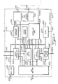
- FIG. 2 shows a block diagram of CRT controller 107.
- a processor interface 207 communicates with processor 104 through lines 111.
- Processor interface 207 and all other blocks within CRT controller 107 are coupled to a data bus 221.
- Processor 104 generally exercises control over data bus 221 through processor interface 207.
- processor interface 207 communicates with a ROM Arbiter 202 and a screen buffer 208.
- Processor 104 controls a keyboard, bell and EEPROM interface 211 through lines 229.
- Processor 104 also sends control signals through processor interface 107, through lines 230 to a controller core 209.
- Processor interface 107 decodes addresses sent from processor 104.
- Screen buffer 208 holes 2K bytes of data, sufficient for one screen of data.
- the data in screen buffer 208 is from processor 104, transferred through data bus 221, to screen buffer 208.
- the data in screen buffer 208 is read by a remote controller 203 through data bus 221.
- Remote controller 203 has two functions. Each function is performed by a state machine within remote controller 203. Upon system reset, remote controller 103 receives a reset signal over reset line 103. Remote controller 203 then acts as an instruction down loader to processor 104. Through address lines 235 remote controller 203 causes ROM arbiter to retrieve data from ROM 106. ROM arbiter 202 returns the retrieved data to remote controller 203 through data bus 221. Through lines 118, remote controller 203 drives the control lines of processor 104, and writes instructions through processor 104 to RAM 105. Once this is complete, control is handed to processor 104 which begins normal firmware execution. The instructions in RAM 105 are used to control processor 104.
- the second function of remote controller 203 is to oversee the transfer of one character row of data (fifteen scan lines) from screen buffer 208 to a row buffer 204. Once every six microseconds, remote controller 203, through lines 118, instructs processor 104 to relinguish control over data bus 221. Remote controller 203 then sends to row buffer 204 through address lines 226 the address within screen buffer 208 of the one row of data to be sent to row buffer 204. Remote controller 203 then controls address lines 222 to direct the transfer of this character row from screen buffer 208 to row buffer 204.
- Row buffer 204 contains two sections. Each section has enough memory to store one character row of data. In a first section, one character row is constantly being read through lines 223 by ROM arbiter 202 and an output enhancement block 205 for the purpose of sending data to CRT 115 to be displayed. In the second section, a character row of data is available for update by remote controller 203. When CRT 115 has completed fifteen scan lines (1 character row), the two sections are switched so that the second section is read by ROM arbiter 202 and output enhancement block 205 and the first section is available for update by remote controller 203.
- ROM arbiter 202 interfaces with ROM 106 through lines 113. For instance, ROM arbiter 202 receives through lines 223 a character from row buffer 204 and receives through lines 224 a scan line number from a controller core 209. With this information ROM arbiter 202 generates an address for the location in ROM 113 of the dot pattern for the scan line of the character received. The ROM address is sent through lines 113 to ROM 106. ROM 106 returns through lines 113 the dot pattern to ROM arbiter 202. ROM arbiter 202 sends the dot pattern to a parallel-to-serial shifter 206 through lines 225.
- the character sent to ROM arbiter 202 from row buffer 204 is also sent through lines 223 to an output enhancement block 205.
- Output enhancement block 205 notes any enhancement, e.g., underlining, italics, bold, etc., and sends an enhancement control signal to shifter 206 through lines 228.
- Parallel-to-serial shifter 206 receives input from ROM arbiter 202 and enhancement control signals from output enhancement block 205 and converts this information to a serial transmission which is sent to CRT 115 through lines 116a. Lines 116a are a subset of lines 116.
- a keyboard, bell and EEPROM interface 211 interfaces with a keyboard through lines 109.
- Keyboard, bell and EEPROM interface interfaces with EEPROM and bell 108 through lines 114.
- Processor 104 is able to access keyboard, bell and EEPROM interface 111 through processor interface 207 through lines 229.
- Controller core 209 provides control and timing for all blocks within CRT controller 107. Controller core 209 keeps track of data displayed on CRT 115, e.g., which row is being scanned, which scan line is being scanned, which character is currently being reproduced. Controller core 209 also informs row buffer 204 through lines 226, when to switch sections. Controller core 209 also generates horizontal synchronization signals and vertical synchronization signals which are sent to CRT 115 through lines 116b. Lines 116b are a subset of lines 116. These signals are used, for example, to fill in blank spots in the display. Further, controller core 209 sends timing information to output enhancement block 205 through lines 227.
- a clock 210 receives a system clock signal through a clock line 231 and generates a clock signal placed on a clock line 232 which is connected to and used by all blocks in CRT controller 107.
- a self test block 201 is accessible to tester circuitry through lines 220. Self test block 201 is used to test operation of CRT controller 107 for manufacturing and other defects.
Landscapes
- Engineering & Computer Science (AREA)
- Theoretical Computer Science (AREA)
- Physics & Mathematics (AREA)
- General Physics & Mathematics (AREA)
- Computer Hardware Design (AREA)
- Human Computer Interaction (AREA)
- General Engineering & Computer Science (AREA)
- Controls And Circuits For Display Device (AREA)
- Digital Computer Display Output (AREA)
- Multi Processors (AREA)
Applications Claiming Priority (2)
| Application Number | Priority Date | Filing Date | Title |
|---|---|---|---|
| US07/238,235 US5148516A (en) | 1988-08-30 | 1988-08-30 | Efficient computer terminal system utilizing a single slave processor |
| US238235 | 1988-08-30 |
Publications (3)
| Publication Number | Publication Date |
|---|---|
| EP0356610A2 true EP0356610A2 (de) | 1990-03-07 |
| EP0356610A3 EP0356610A3 (de) | 1992-07-15 |
| EP0356610B1 EP0356610B1 (de) | 1995-01-25 |
Family
ID=22897029
Family Applications (1)
| Application Number | Title | Priority Date | Filing Date |
|---|---|---|---|
| EP89104085A Expired - Lifetime EP0356610B1 (de) | 1988-08-30 | 1989-03-08 | Computerterminal |
Country Status (6)
| Country | Link |
|---|---|
| US (1) | US5148516A (de) |
| EP (1) | EP0356610B1 (de) |
| JP (1) | JP2760859B2 (de) |
| KR (1) | KR900003730A (de) |
| CA (1) | CA1325684C (de) |
| DE (1) | DE68920800T2 (de) |
Families Citing this family (5)
| Publication number | Priority date | Publication date | Assignee | Title |
|---|---|---|---|---|
| US5499060A (en) * | 1994-01-04 | 1996-03-12 | Texas Instruments Incorporated | System and method for processing video data |
| US5606660A (en) * | 1994-10-21 | 1997-02-25 | Lexar Microsystems, Inc. | Method and apparatus for combining controller firmware storage and controller logic in a mass storage system |
| US20020154102A1 (en) * | 2001-02-21 | 2002-10-24 | Huston James R. | System and method for a programmable color rich display controller |
| US7594135B2 (en) * | 2003-12-31 | 2009-09-22 | Sandisk Corporation | Flash memory system startup operation |
| KR101153118B1 (ko) | 2005-10-12 | 2012-06-07 | 파나소닉 주식회사 | 플라즈마 처리장치 및 플라즈마 처리방법 |
Family Cites Families (53)
| Publication number | Priority date | Publication date | Assignee | Title |
|---|---|---|---|---|
| US4042958A (en) * | 1975-09-10 | 1977-08-16 | Idr, Inc. | Row grabbing system |
| US4099236A (en) * | 1977-05-20 | 1978-07-04 | Intel Corporation | Slave microprocessor for operation with a master microprocessor and a direct memory access controller |
| JPS5438724A (en) * | 1977-09-02 | 1979-03-23 | Hitachi Ltd | Display unit |
| US4342095A (en) * | 1979-04-02 | 1982-07-27 | Harris Corporation | Computer terminal |
| US4414645A (en) * | 1979-04-30 | 1983-11-08 | Honeywell Information Systems Inc. | Hardware-firmware CRT display link system |
| US4245307A (en) * | 1979-09-14 | 1981-01-13 | Formation, Inc. | Controller for data processing system |
| CH637228A5 (fr) * | 1980-03-27 | 1983-07-15 | Willemin Machines Sa | Dispositif de commande d'une machine ou d'une installation. |
| JPS5799686A (en) * | 1980-12-11 | 1982-06-21 | Omron Tateisi Electronics Co | Display controller |
| US4384285A (en) * | 1981-02-19 | 1983-05-17 | Honeywell Information Systems Inc. | Data character video display system with visual attributes |
| US4470042A (en) * | 1981-03-06 | 1984-09-04 | Allen-Bradley Company | System for displaying graphic and alphanumeric data |
| US4403303A (en) * | 1981-05-15 | 1983-09-06 | Beehive International | Terminal configuration manager |
| JPS57212508A (en) * | 1981-06-25 | 1982-12-27 | Mitsubishi Electric Corp | Programming device with cathode ray tube |
| US4481578A (en) * | 1982-05-21 | 1984-11-06 | Pitney Bowes Inc. | Direct memory access data transfer system for use with plural processors |
| US4517654A (en) * | 1982-08-09 | 1985-05-14 | Igt | Video processing architecture |
| US4504828A (en) * | 1982-08-09 | 1985-03-12 | Pitney Bowes Inc. | External attribute logic for use in a word processing system |
| JPS5960480A (ja) * | 1982-09-29 | 1984-04-06 | フアナツク株式会社 | デイスプレイ装置 |
| US4595996A (en) * | 1983-04-25 | 1986-06-17 | Sperry Corporation | Programmable video display character control circuit using multi-purpose RAM for display attributes, character generator, and refresh memory |
| US4665481A (en) * | 1983-06-13 | 1987-05-12 | Honeywell Information Systems Inc. | Speeding up the response time of the direct multiplex control transfer facility |
| JPS6021092A (ja) * | 1983-07-15 | 1985-02-02 | 株式会社東芝 | カラ−インデツクス変換方式 |
| FR2549983B1 (fr) * | 1983-07-25 | 1988-03-18 | Telemecanique Electrique | Terminal pour l'elaboration de programmes utilisables par un automate programmable |
| US4608632A (en) * | 1983-08-12 | 1986-08-26 | International Business Machines Corporation | Memory paging system in a microcomputer |
| IT1159596B (it) * | 1983-08-29 | 1987-03-04 | Olivetti & Co Spa | Apparecchiatura di elaborazione di dati avente un controllore per almeno una periferica di uscita |
| US4646261A (en) * | 1983-09-27 | 1987-02-24 | Motorola Computer Systems, Inc. | Local video controller with video memory update detection scanner |
| US4642789A (en) * | 1983-09-27 | 1987-02-10 | Motorola Computer Systems, Inc. | Video memory controller |
| US4665501A (en) * | 1983-09-30 | 1987-05-12 | Esprit Systems, Inc. | Workstation for local and remote data processing |
| CA1231186A (en) * | 1983-12-20 | 1988-01-05 | Takatoshi Ishii | Display control system |
| EP0383367B1 (de) * | 1983-12-26 | 1999-03-17 | Hitachi, Ltd. | Graphisches Musterverarbeitungsgerät und Verfahren |
| JPS60158482A (ja) * | 1984-01-27 | 1985-08-19 | シャープ株式会社 | Crt表示装置の制御方式 |
| US4613945A (en) * | 1984-05-07 | 1986-09-23 | Pitney Bowes Inc. | Method and apparatus for creating fonts for an electronic character generator |
| US4862156A (en) * | 1984-05-21 | 1989-08-29 | Atari Corporation | Video computer system including multiple graphics controllers and associated method |
| US4663707A (en) * | 1984-05-25 | 1987-05-05 | Scientific Micro Systems, Inc. | Multilevel bootstrap apparatus |
| JPS60254190A (ja) * | 1984-05-31 | 1985-12-14 | 株式会社 アスキ− | デイスプレイコントロ−ラ |
| US4701865A (en) * | 1984-06-25 | 1987-10-20 | Data General Corporation | Video control section for a data processing system |
| GB2162726A (en) * | 1984-07-31 | 1986-02-05 | Ibm | Display of overlapping viewport areas |
| US4851994A (en) * | 1984-08-03 | 1989-07-25 | Sharp Kabushiki Kaisha | Data I/O terminal equipment having mode setting functions for downloading various specified application programs from a host computer |
| US4972273A (en) * | 1984-10-15 | 1990-11-20 | Burkhardt Norman S | High speed, high resolution image processing system |
| US4827254A (en) * | 1984-10-30 | 1989-05-02 | Canon Kabushiki Kaisha | Display apparatus adapted to display various types of modified characters |
| JPS61198331A (ja) * | 1985-02-28 | 1986-09-02 | インタ−ナショナル ビジネス マシ−ンズ コ−ポレ−ション | 表示デ−タ転送制御方法 |
| US4757441A (en) * | 1985-02-28 | 1988-07-12 | International Business Machines Corporation | Logical arrangement for controlling use of different system displays by main proessor and coprocessor |
| JPS61254980A (ja) * | 1985-05-07 | 1986-11-12 | 株式会社ピーエフユー | 文字フオント転送制御方式 |
| JPS6217087A (ja) * | 1985-07-12 | 1987-01-26 | 工業技術院長 | セラミツクスの塑性加工方法 |
| JPH063597B2 (ja) * | 1985-08-20 | 1994-01-12 | 俊明 渡辺 | ワ−ドプロセツサ |
| AU606854B2 (en) * | 1986-01-10 | 1991-02-21 | Wyse Technology, Inc. | Virtual peripheral controller |
| JP2572373B2 (ja) * | 1986-01-14 | 1997-01-16 | 株式会社 アスキ− | カラ−デイスプレイ装置 |
| US4787026A (en) * | 1986-01-17 | 1988-11-22 | International Business Machines Corporation | Method to manage coprocessor in a virtual memory virtual machine data processing system |
| JPS62232006A (ja) * | 1986-04-02 | 1987-10-12 | Yokogawa Electric Corp | ロボツト・システム |
| GB8613153D0 (en) * | 1986-05-30 | 1986-07-02 | Int Computers Ltd | Data display apparatus |
| US4740882A (en) * | 1986-06-27 | 1988-04-26 | Environmental Computer Systems, Inc. | Slave processor for controlling environments |
| KR900005188B1 (ko) * | 1986-07-25 | 1990-07-20 | 후지쓰 가부시끼가이샤 | Crt 콘트롤러 |
| US4907146A (en) * | 1986-10-07 | 1990-03-06 | Giancarlo Caporali | Interactive video network between one master computer and a plurality of slave computers |
| JPH0634209B2 (ja) * | 1987-07-23 | 1994-05-02 | 株式会社日立製作所 | 表示図形検知方式 |
| JPS6459568A (en) * | 1987-08-31 | 1989-03-07 | Nippon Denki Home Electronics | Image information synthesizing system |
| US4965559A (en) * | 1988-05-31 | 1990-10-23 | Motorola, Inc. | Multi-channel graphics controller |
-
1988
- 1988-08-30 US US07/238,235 patent/US5148516A/en not_active Expired - Lifetime
-
1989
- 1989-03-08 EP EP89104085A patent/EP0356610B1/de not_active Expired - Lifetime
- 1989-03-08 DE DE68920800T patent/DE68920800T2/de not_active Expired - Fee Related
- 1989-04-19 CA CA000597144A patent/CA1325684C/en not_active Expired - Fee Related
- 1989-08-29 KR KR1019890012311A patent/KR900003730A/ko not_active Withdrawn
- 1989-08-30 JP JP1224308A patent/JP2760859B2/ja not_active Expired - Fee Related
Also Published As
| Publication number | Publication date |
|---|---|
| EP0356610A3 (de) | 1992-07-15 |
| CA1325684C (en) | 1993-12-28 |
| KR900003730A (ko) | 1990-03-26 |
| DE68920800D1 (de) | 1995-03-09 |
| JPH02113330A (ja) | 1990-04-25 |
| DE68920800T2 (de) | 1995-09-07 |
| JP2760859B2 (ja) | 1998-06-04 |
| EP0356610B1 (de) | 1995-01-25 |
| US5148516A (en) | 1992-09-15 |
Similar Documents
| Publication | Publication Date | Title |
|---|---|---|
| US4644502A (en) | Semiconductor memory device typically used as a video ram | |
| US5001672A (en) | Video ram with external select of active serial access register | |
| US4486856A (en) | Cache memory and control circuit | |
| EP0398510B1 (de) | Video-Direktzugriffsspeicher | |
| US4368461A (en) | Digital data processing device | |
| JP2557113B2 (ja) | デュアルポートダイナミックメモリ | |
| EP0215984B1 (de) | Graphik-Anzeigegerät mit kombiniertem Bitpuffer und Zeichengraphikspeicherung | |
| JPH1091136A (ja) | 電子計算機システム | |
| EP0356610B1 (de) | Computerterminal | |
| EP0166739B1 (de) | Halbleiterspeichervorrichtung für serielle ableseausführungen | |
| US5093902A (en) | Memory control apparatus for accessing an image memory in cycle stealing fashion to read and write videotex signals | |
| JPS6050586A (ja) | ラスタ走査デジタル表示システム | |
| US4970501A (en) | Method for writing data into an image repetition memory of a data display terminal | |
| US5642138A (en) | Display control system using a different clock in the graphics mode from that in the text mode in accessing an image memory | |
| JPH06208787A (ja) | ランダムアクセスメモリ | |
| US4281393A (en) | Programmable computer terminal system | |
| US4625203A (en) | Arrangement for providing data signals for a data display system | |
| EP0182097B1 (de) | Seriell angeschlossenes Videoanpassungsgerät | |
| EP0184080B1 (de) | Farbanzeigesystem | |
| US5309560A (en) | Data selection device | |
| US5467109A (en) | Circuit for generating data of a letter to be displayed on a screen | |
| EP0279662A2 (de) | Schnittstellenschaltung mit Videospeicher | |
| JP3002951B2 (ja) | 画像データ記憶制御装置 | |
| JPS5958475A (ja) | 書込み可能なキヤラクタホントを使用するカラ−グラフイツク陰極線管表示装置 | |
| JPH071425B2 (ja) | ラスタ走査表示システム |
Legal Events
| Date | Code | Title | Description |
|---|---|---|---|
| PUAI | Public reference made under article 153(3) epc to a published international application that has entered the european phase |
Free format text: ORIGINAL CODE: 0009012 |
|
| AK | Designated contracting states |
Kind code of ref document: A2 Designated state(s): DE FR GB IT |
|
| PUAL | Search report despatched |
Free format text: ORIGINAL CODE: 0009013 |
|
| AK | Designated contracting states |
Kind code of ref document: A3 Designated state(s): DE FR GB IT |
|
| 17P | Request for examination filed |
Effective date: 19921127 |
|
| 17Q | First examination report despatched |
Effective date: 19940427 |
|
| GRAA | (expected) grant |
Free format text: ORIGINAL CODE: 0009210 |
|
| AK | Designated contracting states |
Kind code of ref document: B1 Designated state(s): DE FR GB IT |
|
| REF | Corresponds to: |
Ref document number: 68920800 Country of ref document: DE Date of ref document: 19950309 |
|
| ITF | It: translation for a ep patent filed | ||
| ET | Fr: translation filed | ||
| PLBE | No opposition filed within time limit |
Free format text: ORIGINAL CODE: 0009261 |
|
| STAA | Information on the status of an ep patent application or granted ep patent |
Free format text: STATUS: NO OPPOSITION FILED WITHIN TIME LIMIT |
|
| 26N | No opposition filed | ||
| REG | Reference to a national code |
Ref country code: GB Ref legal event code: 732E |
|
| REG | Reference to a national code |
Ref country code: FR Ref legal event code: TP |
|
| REG | Reference to a national code |
Ref country code: GB Ref legal event code: IF02 |
|
| PGFP | Annual fee paid to national office [announced via postgrant information from national office to epo] |
Ref country code: IT Payment date: 20060331 Year of fee payment: 18 |
|
| PGFP | Annual fee paid to national office [announced via postgrant information from national office to epo] |
Ref country code: DE Payment date: 20070430 Year of fee payment: 19 |
|
| PGFP | Annual fee paid to national office [announced via postgrant information from national office to epo] |
Ref country code: GB Payment date: 20080327 Year of fee payment: 20 |
|
| PGFP | Annual fee paid to national office [announced via postgrant information from national office to epo] |
Ref country code: FR Payment date: 20080317 Year of fee payment: 20 |
|
| PG25 | Lapsed in a contracting state [announced via postgrant information from national office to epo] |
Ref country code: DE Free format text: LAPSE BECAUSE OF NON-PAYMENT OF DUE FEES Effective date: 20081001 |
|
| REG | Reference to a national code |
Ref country code: GB Ref legal event code: PE20 Expiry date: 20090307 |
|
| PG25 | Lapsed in a contracting state [announced via postgrant information from national office to epo] |
Ref country code: GB Free format text: LAPSE BECAUSE OF EXPIRATION OF PROTECTION Effective date: 20090307 |
|
| PG25 | Lapsed in a contracting state [announced via postgrant information from national office to epo] |
Ref country code: IT Free format text: LAPSE BECAUSE OF NON-PAYMENT OF DUE FEES Effective date: 20070308 |