EP0357165B1 - Übertragungssystem von Phasenverschiebungsdaten in phasengesteuerten Gruppenantennengeräten - Google Patents
Übertragungssystem von Phasenverschiebungsdaten in phasengesteuerten Gruppenantennengeräten Download PDFInfo
- Publication number
- EP0357165B1 EP0357165B1 EP89250018A EP89250018A EP0357165B1 EP 0357165 B1 EP0357165 B1 EP 0357165B1 EP 89250018 A EP89250018 A EP 89250018A EP 89250018 A EP89250018 A EP 89250018A EP 0357165 B1 EP0357165 B1 EP 0357165B1
- Authority
- EP
- European Patent Office
- Prior art keywords
- data
- phase shift
- phase
- component data
- antenna elements
- Prior art date
- Legal status (The legal status is an assumption and is not a legal conclusion. Google has not performed a legal analysis and makes no representation as to the accuracy of the status listed.)
- Expired - Lifetime
Links
Images


Classifications
-
- H—ELECTRICITY
- H01—ELECTRIC ELEMENTS
- H01Q—ANTENNAS, i.e. RADIO AERIALS
- H01Q3/00—Arrangements for changing or varying the orientation or the shape of the directional pattern of the waves radiated from an antenna or antenna system
- H01Q3/26—Arrangements for changing or varying the orientation or the shape of the directional pattern of the waves radiated from an antenna or antenna system varying the relative phase or relative amplitude of energisation between two or more active radiating elements; varying the distribution of energy across a radiating aperture
- H01Q3/30—Arrangements for changing or varying the orientation or the shape of the directional pattern of the waves radiated from an antenna or antenna system varying the relative phase or relative amplitude of energisation between two or more active radiating elements; varying the distribution of energy across a radiating aperture varying the relative phase between the radiating elements of an array
- H01Q3/34—Arrangements for changing or varying the orientation or the shape of the directional pattern of the waves radiated from an antenna or antenna system varying the relative phase or relative amplitude of energisation between two or more active radiating elements; varying the distribution of energy across a radiating aperture varying the relative phase between the radiating elements of an array by electrical means
- H01Q3/36—Arrangements for changing or varying the orientation or the shape of the directional pattern of the waves radiated from an antenna or antenna system varying the relative phase or relative amplitude of energisation between two or more active radiating elements; varying the distribution of energy across a radiating aperture varying the relative phase between the radiating elements of an array by electrical means with variable phase-shifters
Definitions
- the present invention relates to a phase shift data transfer system for phased array antenna apparatus according to the preamble of claim 1.
- Fig. 1 is a schematic representation of the configuration of a plurality of elements of a commonly used phased array antenna apparatus and the direction of a beam formed by this antenna apparatus.
- a plurality of antenna elements (101, (102), ... (10i), ... (10n) are located on X-Y plane.
- Each antenna element is provided with a phase shifter having a predetermined phase shift capability, so that the phased array antenna apparatus forms a beam in a desired direction.
- the coordinates of a point on a beam in the desired direction are assumed as (X B , Y B , Z B ).
- R is a constant
- the amount of phase shift to be set for antenna elements (101), (102), .... (10n) is sequentially computed in accordance with the equation (1).
- the result of the computation is transferred as phase shift data to the corresponding phase shifter where such data is held until the next new phase shift data is transferred thereto.
- the amount of phase shift to be given to another phase shifter is then computed and the result of the computation is also transferred to the corresponding phase shifter in which it is set.
- the computation of the amount of phase shift is sequentially conducted for every phase shifter. Once obtained, the result of computation is then transferred to a corresponding phase shifter and set and held there until the next new phase shift data is transferred thereto.
- a predetermined amount of phase shift is set for the phase shifter in every antenna element to allow the phased array antenna apparatus to form a beam of radio waves in a desired direction.
- phase shift control for a phased array antenna with the antenna modules arranged in rows and columns is known.
- This phase shift control is provided with central computing means for calculating from the beam direction to be determined and the frequency of the energy emitted, the terms is the mathematical expression for the phase setting for the separate phase shifters in the antenna modules, which terms are the same for all phase shifters, and a computing chip (2) presents in each antenna module for determining the desired phase setting from the terms determined by the central computing means and the position of the separate phase shifters in the array. Due to the relatively complicated computing chips provided in each antenna module this control apparatus is costly to manufacture, especially in case of a large number of antenna elements.
- phase shift data transfer system for phased array antenna apparatus which can eliminate the above-described disadvantages and in which on the one hand the time required to compute the phase shift data and then set a predetermined amount of phase shift in all the phase shifters and on theother hand the complexity of the circuit structure do not increase in proportion to the number of antenna elements.
- the present invention relates to a phase shift data transfer system for a phased array antenna apparatus, comprising: a plurality of antenna elements arranged in a matrix in an X-Y plane, the location of the antenna elements in different columns being represented by different x coordinates and the location of the antenna elements in different rows being represented by different y coordinates; a phase shifting means connected to each of said antenna elements each being given a predetermined amount of phase shift for shifting the phase of a transmit/receive signal; a computing means; and a supply means for supplying data computed by said computing means to the corresponding phase shifting means.
- this system is characterized in that the computing means computes first component data specified by an x coordinate and second component data specified by a y coordinate of an amount of phase shift to be set in each said phase shifting means to form a beam radiating in a desired direction; that the supply means supplies said first and second component data computed by said computing means to the corresponding phase shifting means so as to supply the first component data computed by said computing means to the phase shifting means connected to the antenna elements located in a column having the x coordinate specifying the first component data and to supply the second component data computed by said computing means to the phase shifting means connected to the antenna elements located in a row having the y coordinate specifying the second component data, and that each said phase shifting means is provided with an adder means for determining the sum of said first component data and said second component data, the amount of phase shift corresponding to said sum being set in each said phase shifting means.
- the supply means comprises: first data lines for supplying the first component data to the corresponding phase shifting means connected to the antenna elements located in the columns having the x coordinates specifying the first compnent data; second data lines for supplying the second component data to the corresponding phase shifting means connected to the antenna elements located inthe rows having the y coordinates specifying the second component data; and a transfer controlcircuit for transferring the first and second component data computed by the computing means to the corresponding first and second data lines, respectively.
- Each of the adder means preferably is an adder circuit
- each of the phase shifting means can comprise a first holding circuit for holding the phase shift data output from the adder circuit and a phase shifter in which the phase shift data held in the first holding circuit is set.
- phase shifting means may comprise an input/output control circuit which operates to supply the first component data and the second component data from the computing means to the adder circuit as well as to take out the phase shift data held in the first holding circuit, and a second holding circuit for holding correction data adapted to correct the scattering in phase caused by the difference in electrical length of the transmission/reception system for each antenna element.
- the first component data representing an amount of phase shift to be set in the phase shifters connected to the antenna elements is commonly transferred to the control circuits for the antenna elements at the location represented by the x coordinate specifying the first component data
- the second component data representing an amount of phase shift to be set in the phase shifters connected to the antenna elements is commonly transferred to the control circuits for the antenna elements at the location represented by the y coordinate specifying the second component.
- Each of the control circuits determines the sum of the first and second component data transferred thereto and sets an amount of phase shift corresponding to the resultant sum in the phase shifter. Therefore, the frequency of computation and transfer of all the data on the amounts of phase shift equals the sum of the number of columns and rows in which the antenna elements are arranged.
- the time required to compute the first and second components of one amount of phase shift can be roughly halved as compared to the prior art.
- Fig. 2 is a block diagram illustrating an embodiment of a phase shift data transfer system for phased array antenna apparatuses of the invention.
- the phased array antenna apparatus in Fig. 2 comprises nine antenna elements 1a to 1i arranged in matrix in the X-Y plane as shown in Fig. 1.
- the x coordinate of antenna elements located in the same column are the same, and the y coordinate of antenna elements located in the same row are the same.
- the x coordinate of antenna elements 1a, 1b, 1c is x abc
- the x coordinate of antenna elements 1d, 1e, 1f is x def
- the x coordinate of antenna elements 1g, 1h, 1i is x ghi .
- the y coordinate of antenna elements 1a, 1d, 1g is y adg
- the y coordinate of antenna elements 1b, 1e, 1h is y beh
- the y coordinate of antenna elements 1c, 1f, 1i is y cfi .
- the present embodiment is assumed to employ nine antenna elements. In practice, an extremely large number of antenna elements would be used.
- phase shifters 2a to 2i for changing the phase of a transmit/receive radio wave are connected to antenna elements 1a to 1i, respectively.
- Phase shifters 2a to 2i have control circuits 3a to 3i connected thereto, respectively.
- Control circuits 3a to 3i are adapted to control an amount of phase shift to be set in the corresponding phase shifters, i.e., an amount representing the change in phase of radio waves when changed by the corresponding phase shifters.
- Controllers 3a, 3d, 3g for phase shifters 2a, 2d, 2g connected to antenna elements 1a, 1d, 1g located at y coordinate y adg are commonly connected to one end of Y data line 5a; controllers 3b, 3e, 3h for phase shifters 2b, 2e, 2h connected to antenna elements 1b, 1e, 1h located at y coordinate y beh are commonly connected to one end of Y data line 5b; and controllers 3c, 3f, 3i for phase shifters 2c, 2f, 2i connected to antenna elements 1c, 1f, 1i located at y coordinate y cfi are commonly connected to one end of Y data line 5c.
- X data lines 4a, 4b, 4c and Y date lines 5a, 5b, 5c are connected to a data transfer control circuit 6.
- These X data lines and Y data lines supply X component data and Y component data, respectively, of phase shift data which determine an amount of phase shift to be set in the phase shifters.
- Data transfer control circuit 6 controls transfer of X and Y component data of phase shift data, which determine an amount of phase shift to be set in each phase shifter, to one of X data lines 4a to 4c and to one of Y data lines 5a to 5c.
- control circuits 3a to 3i are commonly connected to data transfer control circuit 6 via clock line 7 which supplies a clock signal for synchronization of the transfer of the X component data and Y component data of the phase shift data which determine amounts of phase shift.
- Phase shift data computing circuit 8 for computing the X and Y component data of the phase shift data is connected to the input of data transfer control circuit 6.
- Phase shifters 2a to 2i are connected to a transmitter/receiver (not shown) via transmission means (not shown) such as cables or strip lines.
- control circuits 3a to 3i in Fig. 2 have the same internal configuration, each comprising an adder circuit for adding the X and Y component data supplied from a corresponding one of X data lines 4a to 4c and a corresponding one of Y data lines 5a to 5c to produce phase shift data and a phase shift data holding circuit for holding the phase shift data computed by the adder circuit.
- the configuration of control circuit 3a is shown in Fig. 3.
- Control circuit 3a comprises an adder circuit 9a and a phase shift data holding circuit 10a.
- X data line 4a for supplying the X component data and Y data line 5a for supplying the Y component data are connected to the input of adder circuit 9a.
- the output of adder circuit 9a is connected to the input of phase shift data holding circuit 10a, whose output is in turn connected to phase shifter 2a.
- Clock line 7 is connected to adder circuit 9a and phase shift data holding circuit 10a.
- phase shift data transfer system for phased array antenna apparatuses thus constructed will next be described.
- ⁇ n k ⁇ x n ⁇ X B + k ⁇ y n ⁇ Y B
- the equation (4) is a modification of the equation (1).
- ⁇ nX k ⁇ x n ⁇ X B
- ⁇ nY k ⁇ y n ⁇ Y B
- n equals a, b, ..., i
- ⁇ n represents an amount of phase shift of the radio waves transmitted or received by antenna element 1n
- k is a constant dependent on the operating frequency
- x n and y n represent the x coordinate and y coordinate of antenna element 1n, respectively.
- X B and Y B respectively represent the x coordinate and y coordinate of point P on a beam radiated in a desired direction and have the relationship represented by equation (2) with Z B , which is the z coordinate of point P.
- the x coordinate of antenna elements 1a,1b, 1c are x abc ; the x coordinate of antenna elements 1d, 1e, 1f are x def ; and the x coordinate of antenna elements 1g, 1h, 1i are x ghi .
- phase shift data computing circuit 8 computes X component data of phase shift data for each of the above x coordinates in accordance with the equation (5) and computes Y component data of the phase shift data for each of the above y coordinates in accordance with the equation (6). The results of these computations are then sent to data transfer control circuit 6.
- data transfer control circuit 6 transfers these X component data and Y component data to control circuits 3a to 3i via the corresponding X data lines 4a to 4c and Y data lines 5a to 5c, respectively, in synchronism with the clock signal supplied through clock line 7.
- X component data k ⁇ x abc ⁇ X B of the phase shift data is supplied to X data line 4a and then transferred to control circuits 3a, 3b, 3c in synchronism with the clock signal on clock line 7;
- X component data k ⁇ x def ⁇ X B of the phase shift data is supplied to X data line 4b and then transferred to control circuits 3d, 3e, 3f in synchronism with the clock signal on clock line 7;
- X component data k ⁇ x ghi ⁇ X B of the phase shift data is supplied to X data line 4c and then transferred to control circuits 3g, 3h, 3i in synchronism with the clock signal on clock line 7.
- Y component data k ⁇ y adg ⁇ Y B of the phase shift data is supplied to Y data line 5a and then transferred to control circuits 3a, 3d, 3g in synchronism with the clock signal on clock line 7;
- Y component data k ⁇ y beh ⁇ Y B of the phase shift data is supplied to Y data line 5b and then transferred to control circuits 3b, 3e, 3h in synchronism with the clock signal on clock line 7;
- Y component data k ⁇ y cfi ⁇ Y B of the phase shift data is supplied to Y data line 5c and then transferred to control circuits 3c, 3f, 3i in synchronism with the clock signal on clock line 7.
- adder circuits 9a to 9i add the X component data and the Y component data of the phase shift data transferred through X data lines 4a to 4c and Y data lines 5a to 5c to compute the phase shift data represented by the equation (4), which are then held in phase shift data holding circuits 10a to 10i, respectively.
- phase shift data k ⁇ x abc ⁇ X B + k ⁇ y adg ⁇ Y B is held in phase shift data holding circuit 10a of control circuit 3a; phase shift data k ⁇ x abc ⁇ X B + k ⁇ y beh ⁇ Y B is held in phase shift data holding circuit 10b of control circuit 3b; phase shift data k ⁇ x abc ⁇ X B + k ⁇ y cfi ⁇ Y B is held in phase shift data holding circuit 10c of control circuit 3c; phase shift data k ⁇ x def ⁇ X B + k ⁇ y adg ⁇ Y B is held in phase shift data holding circuit 10d of control circuit 3d; phase shift data k ⁇ x def ⁇ X B + k ⁇ y beh ⁇ Y B is held in phase shift data holding circuit 10e of control circuit 3e; phase shift data k ⁇ x def ⁇ X B + k ⁇ y cfi ⁇ Y B is held in phase shift data holding circuit 10f of control circuit 3f; phase shift data k ⁇
- phase shift data represented by the equation (4) are held in phase shift data holding circuits 10a to 10i of control circuits 3a to 3i, respectively.
- the phase shift data held in phase shift data holding circuits 10a to 10i are then set in the corresponding phase shifters 2a to 2i to vary the phase of radio waves transmitted or received by antenna elements 1a to 1i in accordance with the predetermined phase shift data.
- the phased array antenna apparatus comprising antenna elements 1a to 1i can form a beam of radio waves in a desired direction.
- the prior art phase shift data transfer system for a phased array antenna apparatus comprising nine antenna elements is disadvantageous in that the computation of phase shift data and the transfer of phase shift data must be respectively conducted nine times.
- the computation of the equations (5) and (6) need only be conducted three times for each, and the transfer of each item of data need only be conducted six times.
- the time required for computation may be halved again.
- Tall (l + m)(Tc/2 + Tt) wherein Tc/2 is the time required to make one computation based on equations (5) and (6), which is half the time Tc [see the equation (3)] required to make one computation in the prior art phase shift data transfer system for a phased array antenna apparatus, and Tt is the time required to transfer X component data or Y component data once for each item of phase shift data.
- T1 l + m l x m ⁇ ( Tc 2 + Tt)
- control circuits 3a to 3i for phase shifters 2a to 2i may be of various circuit forms other than what is shown in Fig. 3.
- the present invention will next be described with reference to control circuit 3a by way of example.
- Fig. 4 shows an embodiment in which control circuit 3a comprises correction data holding circuit 11a.
- the transmission system and the reception system for antenna elements 1a to 1i exhibit some scattering in electrical length.
- Data for correcting scattering in phase due to the scattering in electrical length is held as correction data in correction data holding circuit 11a.
- the phase shift data is computed by adding the X component data from X data line 4a, the Y component data from Y data line 5a and the correction data held in correction data holding circuit 11a.
- the scattering in phase due to the scattering in the transmission system and reception system for antenna elements 1a to 1i can be corrected.
- Fig. 5 shows an example in which control circuit 3a comprises input/output control circuit 12a besides adder circuit 9a and phase shift data holding circuit 10a.
- Input/output control circuit 12a is adapted not only to input the X component data from X data line 4a and the Y component data from Y data line 5a to adder circuit 9a but also to output the phase shift data held in phase shift data holding circuit 10a through either or both of X data line 4a and Y data line 5a to the outside of control circuit 3a. Therefore, when any X component data and Y component data are input to control circuit 3a, it is possible to confirm whether the phase shift data obtained by the addition of these data has been output from control circuit 3a. Thus, it is possible to check if the function of the control circuit 3a is normal or not.
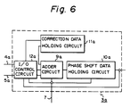
- Fig. 6 shows another example in which control circuit 3a comprises the above-described correction data holding circuit 11a and input/output control circuit 12a, besides adder circuit 9a and phase shift data holding circuit 10a.
- This example is adapted not only to use the correction data held in correction data holding circuit 11a to correct the scattering in phase due to the scattering in electrical length of the transmission system and reception system for antenna element 1a, but also to cause input/output control circuit 12a to output the correction data held in correction data holding circuit 11a through either or both of X data line 4a and Y data line 5a to the outside of control circuit 3a. It is thus possible to confirm if correction data holding circuit 11a operates normally or not.
- the scattering in electrical length of the transmission system and reception system for the antenna elements are not always constant and usually vary. It is thus desirable to be able to correct the scattering in phase every time the electrical length of the transmission system and reception system shows some variation.
- the correction data is given an identification sign indicating that data having this sign is correction data.
- input/output control circuit 12a can identify if the data input from X data line 4a or Y data line 5a is the X component data, Y component data or correction data. If the data input is correction data, this data is transferred to correction data holding circuit 11a which then holds the correction data thus input in place of the data which has so far been held therein and outputs the new correction data to adder circuit 9a.
- correction data holding circuit 11a the correction data for correcting any scattering in phase of the radio wave whenever there is any scattering in electrical length of the transmission system and reception system for antenna elements 1a to 1i or scattering in phase of the radio wave change.
- antenna elements 1a to 1i are arranged in the X-Y plane
- the same effects can be obtained even if antenna elements 1a to 1i are arranged in another coordinate plane.
- the number of antenna elements is arbitrary; the antenna elements can be arranged in any number of columns and rows. It is not necessary for all the intersections of these columns and rows to be filled with antenna elements; some antenna elements can be thinned out regularly or irregularly.
Landscapes
- Variable-Direction Aerials And Aerial Arrays (AREA)
Claims (6)
- Übertragungssystem für Phasenverschiebungsdaten in einem phasengesteuerten Gruppenantennengerät mit:
einer Vielzahl von Antennenelementen (1a-1i), die in einer Matrix in einer X-Y-Ebene angeordnet sind, wobei die Lage der Antennenelemente (1a-1i) in verschiedenen Spalten durch unterschiedliche x-Koordinaten und die Lage der Antennenelemente (1a-1i) in verschiedenen Reihen durch unterschiedliche y-Koordinaten dargestellt ist;
einer Phasenverschiebungsvorrichtung (2a-2i,3a-3i), die mit jedem der Antennenelemente (1a-1i) verbunden ist, wobei jedem ein vorbestimmter Betrag von Phasenverschiebung gegeben ist zum Verschieben der Phase eines Sende/Empfangssignals;
einer Recheneinrichtung (8); und
einer Zuführungseinrichtung (4a-4c,5a-5c,6) zum Zuführen von von der Recheneinrichtung (8) berechneten Daten zu der entsprechenden Phasenverschiebungsvorrichtung (2a-2i,3a-3i),
dadurch gekennzeichnet,
daß
die Recheneinrichtung (8) durch eine x-Koordinate spezifizierte erste Komponentendaten und durch eine y-Koordinate spezifizierte zweite Komponentendaten eines Betrages von Phasenverschiebung berechnet, die in jeder der Phasenverschiebungsvorrichtungen (2a-2i, 3a-3i) einzustellen ist, um einen in einer bestimmten Richtung ausgestrahlten Strahl zu bilden, daß
die Zuführungseinrichtung (4a-4c,5a-5c,6) die von der Recheneinrichtung (8) berechneten ersten und zweiten Komponentendaten zu den entsprechenden Phasenverschiebungsvorrichtungen (2a-2i,3a-3i) führt, derart, daß die von der Recheneinrichtung (8) berechneten ersten Komponentendaten zu den mit den Antennenelementen (z.B. 1a-1c), die sich in einer Spalte mit der die ersten Komponentendaten spezifizierenden x-Koordinate befinden, verbundenen Phasenverschiebungsvorrichtungen (z.B. 2a-2c,3a-3c) geführt werden, und daß die von der Recheneinrichtung berechneten zweiten Komponentendaten zu den mit den Antennenelementen (1a,1d,1g), die sich in einer Reihe mit der die zweiten Komponentendaten spezifizierenden y-Koordinate befinden, verbundenen Phasenverschiebungsvorrichtungen (z.B. 2a,2d,2g,3a,3d,3g) geführt werden, und daß jede der Phasenverschiebungsvorrichtungen (z.B. 2a,3a) mit einer Addiervorrichtung (9a) versehen ist zum Bestimmen der Summe der ersten Komponentendaten und der zweiten Komponentendaten, wobei der Phasenverschiebungsbetrag entsprechend dieser Summe in jeder der Phasenverschiebungsvorrichtungen (z.B. 2a,3a) eingestellt wird. - Übertragungssystem für Phasenverschiebungsdaten nach Anspruch 1, dadurch gekennzeichnet, daß die Zuführungseinrichtung aufweist:
erste Datenleitungen (4a-4c) zum Zuführen der jeweiligen ersten Komponentendaten zu den entsprechenden Phasenverschiebungsvorrichtungen (2a-2i,3a-3i), die mit den Antennenelementen (1a-1i) verbunden sind, die sich in den Spalten mit den die jeweiligen ersten Komponentendaten spezifizierenden x-Koordinaten befinden; zweite Datenleitungen (5a-5c) zum Zuführen der jeweiligen zweiten Komponentendaten zu den entsprechenden Phasenverschiebungsvorrichtungen (2a-2i,3a-3i), die mit den Antennenelementen (1a-1i) verbunden sind, die sich in den Reihen mit den die jeweiligen zweiten Komponentendaten spezifizierenden y-Koordinaten befinden; und eine Übertragungssteuerschaltung (6) zum Übertragen der von der Recheneinrichtung (8) berechneten ersten und zweiten Komponentendaten zu den entsprechenden ersten (4a-4c) und zweiten (5a-5c) Datenleitungen. - Übertragungssystem für Phasenverschiebungsdaten nach Anspruch 2, dadurch gekennzeichnet, daß die Addiervorrichtung eine Addierschaltung (9a) ist und die Phasenverschiebungsvorrichtungen (z.B. 2a,3a) weiterhin eine erste Halteschaltung (10a) zum Halten der von der Addierschaltung (9a) ausgegebenen Phasenverschiebungsdaten und einen Phasenschieber (z.B. 2), in welchem die in der ersten Halteschaltung (10a) gehaltenen Phasenverschiebungsdaten eingestellt werden, aufweisen.
- Übertragungssystem für Phasenverschiebungsdaten nach Anspruch 3, dadurch gekennzeichnet, daß jede der Phasenverschiebungsvorrichtungen (z.B. 2a,3a) weiterhin eine zweite Halteschaltung (11a) zum Halten von Korrekturdaten für die Korrektur etwaiger Streuungen der Phase aufgrund von Streuungen in der elektrischen Länge der Sende- und Empfangssysteme für jedes Antennenelement (z.B. 1a) aufweist, wobei die Addierschaltung (9a) in der Weise tätig ist, daß sie die Korrekturdaten zu den Phasenverschiebungsdaten addiert.
- Übertragungssystem für Phasenverschiebungsdaten nach Anspruch 3, dadurch gekennzeichnet, daß jede Phasenverschiebungsvorrichtung (z.B.2a,3a) weiterhin eine Eingabe/Ausgabe-Steuerschaltung (12a) aufweist, welche die ersten Komponentendaten und die zweiten Komponentendaten von der Recheneinrichtung (8) zu der Addierschaltung (9a) liefert sowie die in den ersten Halteschaltungen (10a) gehaltenen Phaenverschiebungsdaten entnimmt.
- Übertragungssystem für Phasenverschiebungsdaten nach Anspruch 3, dadurch gekennzeichnet, daß jede Phasenverschiebungsvorrichtung (z.B.2a,3a) weiterhin eine Eingabe/Ausgabe-Steuerschaltung (12a), welche die ersten Komponentendaten und die zweiten Komponentendaten von der Recheneinrichtung (8) zu der Addierschaltung (9a) liefert sowie die in den ersten Halteschaltungen (10a) gehaltenen Phasenverschiebungsdaten entnimmt, und eine zweite Halteschaltung (11a) zum Halten von Korrekturdaten für die Korrektur etwaiger Streuungen der Phase aufgrund von Streuungen in der elektrischen Länge der Sende- und Empfangssysteme für jedes Antennenelement (z.B. 1a) aufweist, wobei die Addierschaltung (9a) in der Weise tätig ist, daß sie die Korrekturdaten zu den Phasenverschiebungsdaten addiert.
Applications Claiming Priority (2)
| Application Number | Priority Date | Filing Date | Title |
|---|---|---|---|
| JP217076/88 | 1988-08-31 | ||
| JP63217076A JPH0265401A (ja) | 1988-08-31 | 1988-08-31 | アンテナ制御用データ転送装置 |
Publications (3)
| Publication Number | Publication Date |
|---|---|
| EP0357165A2 EP0357165A2 (de) | 1990-03-07 |
| EP0357165A3 EP0357165A3 (de) | 1991-03-13 |
| EP0357165B1 true EP0357165B1 (de) | 1994-12-28 |
Family
ID=16698456
Family Applications (1)
| Application Number | Title | Priority Date | Filing Date |
|---|---|---|---|
| EP89250018A Expired - Lifetime EP0357165B1 (de) | 1988-08-31 | 1989-08-23 | Übertragungssystem von Phasenverschiebungsdaten in phasengesteuerten Gruppenantennengeräten |
Country Status (4)
| Country | Link |
|---|---|
| US (1) | US4994814A (de) |
| EP (1) | EP0357165B1 (de) |
| JP (1) | JPH0265401A (de) |
| DE (1) | DE68920235T2 (de) |
Families Citing this family (27)
| Publication number | Priority date | Publication date | Assignee | Title |
|---|---|---|---|---|
| JPH07112126B2 (ja) * | 1989-06-07 | 1995-11-29 | 三菱電機株式会社 | アンテナ制御用データ転送装置 |
| GB2241115B (en) * | 1990-02-20 | 1994-08-31 | Gen Electric Co Plc | Multiple-beam energy transmission system |
| JPH0813623B2 (ja) * | 1990-06-18 | 1996-02-14 | 豊田合成株式会社 | フード前端のシール構造 |
| JP2530875Y2 (ja) * | 1990-10-04 | 1997-04-02 | 三菱電機株式会社 | アンテナ制御用データ転送装置 |
| JP2530876Y2 (ja) * | 1990-10-04 | 1997-04-02 | 三菱電機株式会社 | アンテナ制御用データ転送装置 |
| FR2672436B1 (fr) * | 1991-01-31 | 1993-09-10 | Europ Agence Spatiale | Dispositif de controle electronique du diagramme de rayonnement d'une antenne a un ou plusieurs faisceaux de direction et/ou de largeur variable. |
| US5333001A (en) * | 1993-05-18 | 1994-07-26 | Martin Marietta Corporation | Multifrequency antenna array |
| US5353031A (en) * | 1993-07-23 | 1994-10-04 | Itt Corporation | Integrated module controller |
| DE69533934T2 (de) | 1994-11-04 | 2005-12-01 | Andrew Corp., Orland Park | Basisstation für zellulares Telekommunikationssystem, Verfahren zur Keulenabwärtsneigung und Antennensteuerungsanordnung |
| US6255990B1 (en) * | 1998-05-12 | 2001-07-03 | Riverside Research Institute | Processor for two-dimensional array antenna |
| JP3481482B2 (ja) * | 1998-12-24 | 2003-12-22 | 日本電気株式会社 | フェーズドアレイアンテナおよびその製造方法 |
| US6239744B1 (en) | 1999-06-30 | 2001-05-29 | Radio Frequency Systems, Inc. | Remote tilt antenna system |
| US6824307B2 (en) | 2000-12-12 | 2004-11-30 | Harris Corporation | Temperature sensor and related methods |
| US6573863B2 (en) | 2000-12-12 | 2003-06-03 | Harris Corporation | Phased array antenna system utilizing highly efficient pipelined processing and related methods |
| US6573862B2 (en) | 2000-12-12 | 2003-06-03 | Harris Corporation | Phased array antenna including element control device providing fault detection and related methods |
| US6593881B2 (en) | 2000-12-12 | 2003-07-15 | Harris Corporation | Phased array antenna including an antenna module temperature sensor and related methods |
| US6587077B2 (en) | 2000-12-12 | 2003-07-01 | Harris Corporation | Phased array antenna providing enhanced element controller data communication and related methods |
| US6690324B2 (en) | 2000-12-12 | 2004-02-10 | Harris Corporation | Phased array antenna having reduced beam settling times and related methods |
| US6522293B2 (en) | 2000-12-12 | 2003-02-18 | Harris Corporation | Phased array antenna having efficient compensation data distribution and related methods |
| US6473037B2 (en) | 2000-12-12 | 2002-10-29 | Harris Corporation | Phased array antenna system having prioritized beam command and data transfer and related methods |
| US6522294B2 (en) | 2000-12-12 | 2003-02-18 | Harris Corporation | Phased array antenna providing rapid beam shaping and related methods |
| DE10104564C1 (de) | 2001-02-01 | 2002-09-19 | Kathrein Werke Kg | Steuerungsvorrichtung zum Einstellen eines unterschiedlichen Absenkwinkels insbesondere von zu einer Basisstation gehörenden Mobilfunkantennen sowie eine zugehörige Antenne und Verfahren zur Veränderung eines Absenkwinkels |
| US6573875B2 (en) | 2001-02-19 | 2003-06-03 | Andrew Corporation | Antenna system |
| US6646600B2 (en) | 2001-11-09 | 2003-11-11 | Harris Corporation | Phased array antenna with controllable amplifier bias adjustment and related methods |
| US6496143B1 (en) | 2001-11-09 | 2002-12-17 | Harris Corporation | Phased array antenna including a multi-mode element controller and related method |
| US7557675B2 (en) | 2005-03-22 | 2009-07-07 | Radiacion Y Microondas, S.A. | Broad band mechanical phase shifter |
| CN115000708B (zh) * | 2022-05-27 | 2024-06-18 | 中国电子科技集团公司第十研究所 | 一种有源相控阵天线波束状态的简化配置方法 |
Family Cites Families (7)
| Publication number | Priority date | Publication date | Assignee | Title |
|---|---|---|---|---|
| DE2062896C3 (de) * | 1970-12-21 | 1978-11-23 | Siemens Ag, 1000 Berlin Und 8000 Muenchen | Verfahren zur Phasenberechnung für eine mit elektronischer Strahlschwenkung arbeitende Antenne |
| FR2235503B1 (de) * | 1973-06-28 | 1978-10-27 | Siemens Ag | |
| JPS5418655A (en) * | 1977-07-13 | 1979-02-10 | Mitsubishi Electric Corp | Phase array antenna |
| US4445119A (en) * | 1981-04-30 | 1984-04-24 | Raytheon Company | Distributed beam steering computer |
| NL8303444A (nl) * | 1983-10-07 | 1985-05-01 | Hollandse Signaalapparaten Bv | Fasedraaier-sturing voor een phased-array antenne. |
| FR2560447B1 (fr) * | 1984-02-24 | 1988-04-08 | Thomson Csf | Antenne reseau et radar de sensibilite reduite au brouillage |
| JPS6348903A (ja) * | 1986-08-19 | 1988-03-01 | Mitsubishi Electric Corp | アンテナ装置 |
-
1988
- 1988-08-31 JP JP63217076A patent/JPH0265401A/ja active Pending
-
1989
- 1989-08-17 US US07/395,443 patent/US4994814A/en not_active Expired - Lifetime
- 1989-08-23 DE DE68920235T patent/DE68920235T2/de not_active Expired - Fee Related
- 1989-08-23 EP EP89250018A patent/EP0357165B1/de not_active Expired - Lifetime
Also Published As
| Publication number | Publication date |
|---|---|
| EP0357165A2 (de) | 1990-03-07 |
| EP0357165A3 (de) | 1991-03-13 |
| JPH0265401A (ja) | 1990-03-06 |
| US4994814A (en) | 1991-02-19 |
| DE68920235D1 (de) | 1995-02-09 |
| DE68920235T2 (de) | 1995-08-31 |
Similar Documents
| Publication | Publication Date | Title |
|---|---|---|
| US4994814A (en) | Phase shift data transfer system for phased array antenna apparatuses | |
| CN110940957B (zh) | 一种模块化毫米波雷达 | |
| EP1329983B1 (de) | Anordnung und Methode zur Kalibrierung einer Gruppenantenne | |
| US4445119A (en) | Distributed beam steering computer | |
| US6606056B2 (en) | Beam steering controller for a curved surface phased array antenna | |
| RU2729975C2 (ru) | Система фазированной антенной решетки, имеющая модульную архитектуру для управления и мониторинга | |
| EP2273614B1 (de) | Verfahren und Vorrichtung zur Feldkalibrierung einer Phasenarray-Antenne | |
| EP3584952B1 (de) | Basisstationtestsystem und -verfahren auf basis von 3d-massivem mimo und speichermedium | |
| US6762717B2 (en) | Apparatus and method for calibrating array antenna | |
| US5105198A (en) | Method of determining a position using satellites | |
| EP0397916B1 (de) | Verteiltes System zur Strahlsteuerungsregelung für eine ebene Gruppenantenne mit Flugzeug-Rollkompensation | |
| KR102061620B1 (ko) | 위상 배열 안테나 모듈, 이를 포함하는 위상 배열 안테나 시스템 및 이를 이용한 신호 보정 방법 | |
| US3646558A (en) | Phased array beam steering control with phase misalignment correction | |
| US5130717A (en) | Antenna having elements with programmable digitally generated time delays | |
| US9948408B1 (en) | Antenna array calibration | |
| CN114384479A (zh) | 相控阵雷达幅相校准方法、装置及存储介质 | |
| US3710329A (en) | Phase control circuits using frequency multiplication for phased array antennas | |
| EP0247780B1 (de) | Echtzeitanzeige der Strahlrichtung bei einer Anordnung zur Antennenstrahlsteuerung | |
| EP0137562A2 (de) | Phasenschiebersteuerung bei einer Gruppenantenne | |
| US20230261360A1 (en) | Radar apparatus comprising multiple antennas | |
| JPH1117434A (ja) | 空間給電型フェーズドアレイアンテナ装置 | |
| US20050017917A1 (en) | Apparatus for tracing an optimal direction to receive satellite signal in active phase array antenna system | |
| US4817001A (en) | Method of correcting navigation system errors caused by drift | |
| US20240264262A1 (en) | Measurement apparatus | |
| JPH0427206Y2 (de) |
Legal Events
| Date | Code | Title | Description |
|---|---|---|---|
| PUAI | Public reference made under article 153(3) epc to a published international application that has entered the european phase |
Free format text: ORIGINAL CODE: 0009012 |
|
| AK | Designated contracting states |
Kind code of ref document: A2 Designated state(s): DE FR GB |
|
| PUAL | Search report despatched |
Free format text: ORIGINAL CODE: 0009013 |
|
| 17P | Request for examination filed |
Effective date: 19901231 |
|
| AK | Designated contracting states |
Kind code of ref document: A3 Designated state(s): DE FR GB |
|
| 17Q | First examination report despatched |
Effective date: 19930809 |
|
| GRAA | (expected) grant |
Free format text: ORIGINAL CODE: 0009210 |
|
| AK | Designated contracting states |
Kind code of ref document: B1 Designated state(s): DE FR GB |
|
| REF | Corresponds to: |
Ref document number: 68920235 Country of ref document: DE Date of ref document: 19950209 |
|
| ET | Fr: translation filed | ||
| PLBE | No opposition filed within time limit |
Free format text: ORIGINAL CODE: 0009261 |
|
| STAA | Information on the status of an ep patent application or granted ep patent |
Free format text: STATUS: NO OPPOSITION FILED WITHIN TIME LIMIT |
|
| 26N | No opposition filed | ||
| REG | Reference to a national code |
Ref country code: GB Ref legal event code: 746 Effective date: 19960611 |
|
| REG | Reference to a national code |
Ref country code: FR Ref legal event code: D6 |
|
| REG | Reference to a national code |
Ref country code: GB Ref legal event code: IF02 |
|
| PGFP | Annual fee paid to national office [announced via postgrant information from national office to epo] |
Ref country code: FR Payment date: 20060808 Year of fee payment: 18 |
|
| PGFP | Annual fee paid to national office [announced via postgrant information from national office to epo] |
Ref country code: DE Payment date: 20060817 Year of fee payment: 18 |
|
| PGFP | Annual fee paid to national office [announced via postgrant information from national office to epo] |
Ref country code: GB Payment date: 20060823 Year of fee payment: 18 |
|
| GBPC | Gb: european patent ceased through non-payment of renewal fee |
Effective date: 20070823 |
|
| REG | Reference to a national code |
Ref country code: FR Ref legal event code: ST Effective date: 20080430 |
|
| PG25 | Lapsed in a contracting state [announced via postgrant information from national office to epo] |
Ref country code: DE Free format text: LAPSE BECAUSE OF NON-PAYMENT OF DUE FEES Effective date: 20080301 |
|
| PG25 | Lapsed in a contracting state [announced via postgrant information from national office to epo] |
Ref country code: FR Free format text: LAPSE BECAUSE OF NON-PAYMENT OF DUE FEES Effective date: 20070831 |
|
| PG25 | Lapsed in a contracting state [announced via postgrant information from national office to epo] |
Ref country code: GB Free format text: LAPSE BECAUSE OF NON-PAYMENT OF DUE FEES Effective date: 20070823 |