EP0357346A2 - Circuit intégré du type CMOS ayant une isolation modifiée - Google Patents
Circuit intégré du type CMOS ayant une isolation modifiée Download PDFInfo
- Publication number
- EP0357346A2 EP0357346A2 EP89308621A EP89308621A EP0357346A2 EP 0357346 A2 EP0357346 A2 EP 0357346A2 EP 89308621 A EP89308621 A EP 89308621A EP 89308621 A EP89308621 A EP 89308621A EP 0357346 A2 EP0357346 A2 EP 0357346A2
- Authority
- EP
- European Patent Office
- Prior art keywords
- channel
- region
- type region
- type
- implant
- Prior art date
- Legal status (The legal status is an assumption and is not a legal conclusion. Google has not performed a legal analysis and makes no representation as to the accuracy of the status listed.)
- Granted
Links
Images

Classifications
-
- H—ELECTRICITY
- H10—SEMICONDUCTOR DEVICES; ELECTRIC SOLID-STATE DEVICES NOT OTHERWISE PROVIDED FOR
- H10D—INORGANIC ELECTRIC SEMICONDUCTOR DEVICES
- H10D84/00—Integrated devices formed in or on semiconductor substrates that comprise only semiconducting layers, e.g. on Si wafers or on GaAs-on-Si wafers
- H10D84/01—Manufacture or treatment
- H10D84/0123—Integrating together multiple components covered by H10D12/00 or H10D30/00, e.g. integrating multiple IGBTs
- H10D84/0126—Integrating together multiple components covered by H10D12/00 or H10D30/00, e.g. integrating multiple IGBTs the components including insulated gates, e.g. IGFETs
- H10D84/0165—Integrating together multiple components covered by H10D12/00 or H10D30/00, e.g. integrating multiple IGBTs the components including insulated gates, e.g. IGFETs the components including complementary IGFETs, e.g. CMOS devices
- H10D84/0188—Manufacturing their isolation regions
-
- H—ELECTRICITY
- H10—SEMICONDUCTOR DEVICES; ELECTRIC SOLID-STATE DEVICES NOT OTHERWISE PROVIDED FOR
- H10D—INORGANIC ELECTRIC SEMICONDUCTOR DEVICES
- H10D84/00—Integrated devices formed in or on semiconductor substrates that comprise only semiconducting layers, e.g. on Si wafers or on GaAs-on-Si wafers
- H10D84/01—Manufacture or treatment
- H10D84/02—Manufacture or treatment characterised by using material-based technologies
- H10D84/03—Manufacture or treatment characterised by using material-based technologies using Group IV technology, e.g. silicon technology or silicon-carbide [SiC] technology
- H10D84/038—Manufacture or treatment characterised by using material-based technologies using Group IV technology, e.g. silicon technology or silicon-carbide [SiC] technology using silicon technology, e.g. SiGe
-
- H—ELECTRICITY
- H10—SEMICONDUCTOR DEVICES; ELECTRIC SOLID-STATE DEVICES NOT OTHERWISE PROVIDED FOR
- H10W—GENERIC PACKAGES, INTERCONNECTIONS, CONNECTORS OR OTHER CONSTRUCTIONAL DETAILS OF DEVICES COVERED BY CLASS H10
- H10W10/00—Isolation regions in semiconductor bodies between components of integrated devices
- H10W10/01—Manufacture or treatment
- H10W10/011—Manufacture or treatment of isolation regions comprising dielectric materials
- H10W10/012—Manufacture or treatment of isolation regions comprising dielectric materials using local oxidation of silicon [LOCOS]
- H10W10/0125—Manufacture or treatment of isolation regions comprising dielectric materials using local oxidation of silicon [LOCOS] comprising introducing electrical impurities in local oxidation regions, e.g. to alter LOCOS oxide growth characteristics
- H10W10/0126—Manufacture or treatment of isolation regions comprising dielectric materials using local oxidation of silicon [LOCOS] comprising introducing electrical impurities in local oxidation regions, e.g. to alter LOCOS oxide growth characteristics introducing electrical active impurities in local oxidation regions to create channel stoppers
- H10W10/0127—Manufacture or treatment of isolation regions comprising dielectric materials using local oxidation of silicon [LOCOS] comprising introducing electrical impurities in local oxidation regions, e.g. to alter LOCOS oxide growth characteristics introducing electrical active impurities in local oxidation regions to create channel stoppers using both n-type and p-type impurities, e.g. for isolation of complementary doped regions
-
- H—ELECTRICITY
- H10—SEMICONDUCTOR DEVICES; ELECTRIC SOLID-STATE DEVICES NOT OTHERWISE PROVIDED FOR
- H10W—GENERIC PACKAGES, INTERCONNECTIONS, CONNECTORS OR OTHER CONSTRUCTIONAL DETAILS OF DEVICES COVERED BY CLASS H10
- H10W10/00—Isolation regions in semiconductor bodies between components of integrated devices
- H10W10/10—Isolation regions comprising dielectric materials
- H10W10/13—Isolation regions comprising dielectric materials formed using local oxidation of silicon [LOCOS], e.g. sealed interface localised oxidation [SILO] or side-wall mask isolation [SWAMI]
-
- H—ELECTRICITY
- H10—SEMICONDUCTOR DEVICES; ELECTRIC SOLID-STATE DEVICES NOT OTHERWISE PROVIDED FOR
- H10D—INORGANIC ELECTRIC SEMICONDUCTOR DEVICES
- H10D84/00—Integrated devices formed in or on semiconductor substrates that comprise only semiconducting layers, e.g. on Si wafers or on GaAs-on-Si wafers
- H10D84/80—Integrated devices formed in or on semiconductor substrates that comprise only semiconducting layers, e.g. on Si wafers or on GaAs-on-Si wafers characterised by the integration of at least one component covered by groups H10D12/00 or H10D30/00, e.g. integration of IGFETs
- H10D84/82—Integrated devices formed in or on semiconductor substrates that comprise only semiconducting layers, e.g. on Si wafers or on GaAs-on-Si wafers characterised by the integration of at least one component covered by groups H10D12/00 or H10D30/00, e.g. integration of IGFETs of only field-effect components
- H10D84/83—Integrated devices formed in or on semiconductor substrates that comprise only semiconducting layers, e.g. on Si wafers or on GaAs-on-Si wafers characterised by the integration of at least one component covered by groups H10D12/00 or H10D30/00, e.g. integration of IGFETs of only field-effect components of only insulated-gate FETs [IGFET]
- H10D84/85—Complementary IGFETs, e.g. CMOS
- H10D84/859—Complementary IGFETs, e.g. CMOS comprising both N-type and P-type wells, e.g. twin-tub
Definitions
- This invention relates to semiconductor integrated circuits having both n-channel and p-channel devices.
- CMOS complementary metal-oxide-semiconductor
- This configuration obtained its name because it uses both p-channel and n-channel insulated gate field effect transistors.
- the n-channel and p-channel devices should be electrically isolated from each other, and are therefore frequently formed in "tubs", which are doped regions in a silicon substrate.
- tubs One method of forming the tubs is shown in U.S. patent 4,554,726, co-assigned herewith. In that technique, a photoresist is patterned to expose portions of the substrate for the n-type tubs.
- Phosphorus and arsenic are implanted, followed by photoresist stripping and oxidation of the n-type tub surface. Boron is then implanted for the p-type tub, and the oxide stripped. A dopant drive-in heating step is then accomplished to drive the dopants deeper into the semiconductor substrate, thereby forming the n-type and p-type tubs.
- a second boro implant into the p tubs is performed; subsequent lithography then defines an opening in a masking layer at the boundary between the n and p tubs.
- An oxidation step follows, to form the "field oxide” regions, which isolate the n tubs from the p tubs at the surface of the substrate.
- the second boron implant then forms the "channel stop" region under the field oxide in the p tub, which aids in isolating the n-channel devices to be formed therein.
- the field oxide is formed during a relatively brief oxidation process that is accomplished in steam at high pressure. Further fabrication steps to from the p-channel and n-channel field effect transistors (in the n tubs and p tubs, respectively) follow the tub formation, according to techniques well known to those skilled in the art.
- CMOS structure improved characteristics with a CMOS structure can be obtained by using a channel stop implant of boron at a depth at least as great as the depth of the field oxide in the silicon substrate. That is, the p-type channel stop implant has an energy selected so that the peak concentration is just below the subsequently formed field oxide.
- both the electrical isolation of the n-channel devices, and the punch-through characteristics may be simultaneously improved by this technique, facilitating the use of the CMOS process in sub-micron geometries.
- the present invention concerns an improved method of forming integrated circuits having both p channel and n channel devices.
- a CMOS integrated circuit is shown in an early stage of fabrication. Depicted are substrate 1, oxide layer 3 and photoresist layer 5. The photoresist and oxide layers were patterned to expose selected portions of the substrate for the ion implantation for the n-type tub. Both a phosphorus implant 7 and an arsenic implant 9 have been made, as indicated by the open triangles and x's, respectively. As will be readily apparent to those skilled in the art, these steps can be readily performed by a skilled artisan without further description. The photoresist and oxide are stripped and an oxidation step for the n-type tub is performed.
- the oxide is shown as region 11, and the n-type region as 13.
- a first boron implant for the p-tub is performed, shown by dots 20. This implant may be either shallow or deep.
- a tub drive-in step is then performed, producing the n tub 15 and the p tub 17, as shown in FIG. 3.
- the tub drive-in is followed by a second boron implantation, shown as open squares 30.
- the second boron implant is the "deep" p-type implant according to the present invention. This places the peak boron concentration as implanted at a depth in the substrate slightly greater than the depth of the subsequently-formed field oxide. Consequently, the amount of boron segregation to the field oxide during the subsequent steam oxidation is also reduced.
- the result is improved isolation for the n-channel devices subsequently formed in the p tub.
- the n-type tub oxide 11 is stripped. Active region patterning and high pressure field oxidation are performed.
- the resulting structure is shown in FIG. 4, with a thin oxide shown as region 19 and the field oxide shown as region 21.
- the above-noted second, "deep" boron implant has an energy selected so that the peak of the boron profile will be located immediately underneath the field oxide, after the subsequent oxidation step.
- This energy also creates a retrograde p-tub boron profile in the channel region. That is, the peak concentration is below the substrate surface in the channel region. The peak should be close to the junction depth to improve punch through resistance. It will also be appreciated by those skilled in the art that the use of high pressure steam oxidation to grow the field oxide reduces the thermal cycle, and therefore creates less boron segregation into the field oxide.
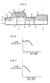
- FIG. 5 shows the structure after device fabrication, as well as the adjoining field oxide region.
- substrate 51 lightly doped source/drain regions 53, heavily doped source/drain regions 55, and source/drain silicide contact regions 57.
- polysilicon gate region 59 and gate silicide contact region 61 silicon dioxide gate sidewalls 63, and field oxide 65.
- gate oxide 67 under the polysilicon gate 59, with the channel region being located immediately under the gate oxide in the substrate.
- the approximate depth of the peak concentration of the second boron implant noted above is indicated by dashed line 66. As can be seen, the peak lies just under the field oxide region 65 for improved channel stop isolation.
- the peak of the boron implant helps prevent punch-through between the heavily doped source/drain regions 55.
- the boron concentration profiles along lines (A) and (B) of FIG. 5, which are through the gate structure and the field oxide, respectively, are shown in FIG. 6 and 7, respectively, with the boron concentration plotted vertically and the depth horizontally.
- the units for both are arbitrary units.
- the boron concentration in the channel region i.e., directly under the gate oxide
- an optional third boron implant which is referred to as a "threshold adjustment" implant in the art, and is a known technique used to raise the threshold voltage of the n-channel device.
- this adjustment is not necessary in all devices, and may be accomplished by other means, such as a p-doped polysilicon gate.
- the threshold adjustment implant is accomplished using BF2 at a beam energy of 50 KeV, at a dose of 1.7x10¹²/cm2.
- the boron concentration then decreases from this high value at the surface to a minimum at d1, and then increases to the peak at d2 before again decreasing.
- the peak at d2 is due to the "deep" second boron implant noted above, and the increase between d1 and d2 is the "retrograde" profile referred to herein.
- the boron concentration in the field oxide region has a maximum at the oxide-substrate interface and continually decreases with depth into the substrate.
- the depth to which the "deep" boron implant should be accomplished therefore depends on the desired field oxide thickness.
- allowance is made for the greater thickness of silicon dioxide as compared to the silicon consumed in its formation. That is, a given thickness of grown SiO2 consumes about 40 percent as much thickness of the silicon substrate.
- a field oxide region 65 having a thickness of 630 nanometers (6300) angstroms) consumes about 250 nanometers (2500 angstroms) of the silicon substrate.
- Such a thickness may be grown at a pressure of 25 atmospheres in steam, at a temperature of 900 degrees centrigrade for 25 minutes. Therefore, the boron energy is selected to implant to a depth of slightly greater than 250 nanometers.
- a typical boron dose for this implant is 2.5x10¹²/cm2.
- Other energies and dosages will be easily selected by those skilled in the art as device design varies and continues to evolve.
- the field oxide thickness as grown will be greater than 450 nanometers (4500 angstroms), thereby consuming at least 180 nanometers (1800 angstroms) of silicon.
- the implant depth according to the present technique will typically be at least 200 nanometers, and more typically at least 250 nanometers.
- a reduction in power supply voltage below the current 5 volt standard may allow for thinner field oxide regions.
- the depth referred to is from the silicon surface as implanted, prior to field oxide growth, and remains substantially this same value underneath the gate oxide fo the n-channel devices.
- the field oxide is typically subjected to an etch-back procedure to reduce the "birds-beak" effect, so that the field oxide thickness on the final device is typically only about two-thirds of the thicknesses as grown.
- twin-tub CMOS process wherein additional p and n dopants are used to define the two tub regions in a relatively lightly doped substrate (either n-type or p-type).
- the present invention may also be used with a single p-type tub formed in an n-type substrate. That technique is often referred to as a "single well" or “single tub” process, and the n-doped substrate then forms the region in which the p-channel devices are formed. Still other variations are possible.
Landscapes
- Metal-Oxide And Bipolar Metal-Oxide Semiconductor Integrated Circuits (AREA)
- Insulated Gate Type Field-Effect Transistor (AREA)
- Element Separation (AREA)
Applications Claiming Priority (2)
| Application Number | Priority Date | Filing Date | Title |
|---|---|---|---|
| US07/238,362 US5045898A (en) | 1988-08-30 | 1988-08-30 | CMOS integrated circuit having improved isolation |
| US238362 | 1988-08-30 |
Publications (3)
| Publication Number | Publication Date |
|---|---|
| EP0357346A2 true EP0357346A2 (fr) | 1990-03-07 |
| EP0357346A3 EP0357346A3 (fr) | 1991-09-25 |
| EP0357346B1 EP0357346B1 (fr) | 1997-10-22 |
Family
ID=22897539
Family Applications (1)
| Application Number | Title | Priority Date | Filing Date |
|---|---|---|---|
| EP89308621A Expired - Lifetime EP0357346B1 (fr) | 1988-08-30 | 1989-08-24 | Circuit intégré du type CMOS ayant une isolation modifiée |
Country Status (6)
| Country | Link |
|---|---|
| US (1) | US5045898A (fr) |
| EP (1) | EP0357346B1 (fr) |
| JP (1) | JPH02112273A (fr) |
| CA (1) | CA1315419C (fr) |
| DE (1) | DE68928396T2 (fr) |
| ES (1) | ES2109222T3 (fr) |
Cited By (3)
| Publication number | Priority date | Publication date | Assignee | Title |
|---|---|---|---|---|
| WO1998006137A1 (fr) * | 1996-08-07 | 1998-02-12 | Advanced Micro Devices, Inc. | Region de drain selectivement dopee pour une intensite de saturation de drain accrue et procede de realisation de ladite intensite |
| US6188106B1 (en) | 1998-09-03 | 2001-02-13 | Advanced Micro Devices, Inc. | MOSFET having a highly doped channel liner and a dopant seal to provide enhanced device properties |
| US6362510B1 (en) | 1998-12-07 | 2002-03-26 | Advanced Micro Devices, Inc. | Semiconductor topography having improved active device isolation and reduced dopant migration |
Families Citing this family (15)
| Publication number | Priority date | Publication date | Assignee | Title |
|---|---|---|---|---|
| JP2924395B2 (ja) * | 1992-01-09 | 1999-07-26 | 日本電気株式会社 | 半導体装置の製造方法 |
| US5344787A (en) * | 1993-09-24 | 1994-09-06 | Vlsi Technology, Inc. | Latid implants for increasing the effective width of transistor elements in a semiconductor device |
| US5409848A (en) * | 1994-03-31 | 1995-04-25 | Vlsi Technology, Inc. | Angled lateral pocket implants on p-type semiconductor devices |
| US7348227B1 (en) * | 1995-03-23 | 2008-03-25 | Semiconductor Energy Laboratory Co., Ltd. | Semiconductor device and manufacturing method thereof |
| US5650350A (en) * | 1995-08-11 | 1997-07-22 | Micron Technology, Inc. | Semiconductor processing method of forming a static random access memory cell and static random access memory cell |
| US7064376B2 (en) * | 1996-05-24 | 2006-06-20 | Jeng-Jye Shau | High performance embedded semiconductor memory devices with multiple dimension first-level bit-lines |
| US5748547A (en) * | 1996-05-24 | 1998-05-05 | Shau; Jeng-Jye | High performance semiconductor memory devices having multiple dimension bit lines |
| US20050036363A1 (en) * | 1996-05-24 | 2005-02-17 | Jeng-Jye Shau | High performance embedded semiconductor memory devices with multiple dimension first-level bit-lines |
| US6083795A (en) * | 1998-02-09 | 2000-07-04 | Taiwan Semiconductor Manufacturing Company | Large angle channel threshold implant for improving reverse narrow width effect |
| US6144076A (en) * | 1998-12-08 | 2000-11-07 | Lsi Logic Corporation | Well formation For CMOS devices integrated circuit structures |
| FR2794898B1 (fr) | 1999-06-11 | 2001-09-14 | France Telecom | Dispositif semi-conducteur a tension de seuil compensee et procede de fabrication |
| US6812521B1 (en) | 1999-11-16 | 2004-11-02 | Advanced Micro Devices, Inc. | Method and apparatus for improved performance of flash memory cell devices |
| US9401274B2 (en) | 2013-08-09 | 2016-07-26 | Taiwan Semiconductor Manufacturing Company Limited | Methods and systems for dopant activation using microwave radiation |
| FI127168B (en) * | 2014-05-20 | 2017-12-29 | Murata Manufacturing Co | Method for making a MEMS structure and use of the method |
| DE102015106397B4 (de) * | 2015-04-16 | 2019-08-22 | Taiwan Semiconductor Manufacturing Company, Ltd. | Verfahren und Systeme zur Dotierstoffaktivierung mithilfe von Mikrowellenbestrahlung |
Citations (4)
| Publication number | Priority date | Publication date | Assignee | Title |
|---|---|---|---|---|
| US4471523A (en) | 1983-05-02 | 1984-09-18 | International Business Machines Corporation | Self-aligned field implant for oxide-isolated CMOS FET |
| EP0123182A1 (fr) | 1983-04-21 | 1984-10-31 | Siemens Aktiengesellschaft | Procédé pour la fabrication de circuits intégrés à haute densité comportant des transistors à effet de champ du type MOS complémentaires |
| WO1985004984A1 (fr) | 1984-04-17 | 1985-11-07 | American Telephone & Telegraph Company | Technologie des circuits integres cmos |
| WO1997005443A1 (fr) | 1995-07-26 | 1997-02-13 | Laser Products Corporation | Systemes d'etuis pour armes de main |
Family Cites Families (9)
| Publication number | Priority date | Publication date | Assignee | Title |
|---|---|---|---|---|
| JPS5379474A (en) * | 1976-12-24 | 1978-07-13 | Matsushita Electric Ind Co Ltd | Manufacture of semiconductor device |
| US4354307A (en) * | 1979-12-03 | 1982-10-19 | Burroughs Corporation | Method for mass producing miniature field effect transistors in high density LSI/VLSI chips |
| JPS5965481A (ja) * | 1982-10-06 | 1984-04-13 | Nec Corp | 半導体装置 |
| DE3467953D1 (en) * | 1983-04-21 | 1988-01-14 | Toshiba Kk | Semiconductor device having an element isolation layer and method of manufacturing the same |
| JPS5925242A (ja) * | 1983-07-11 | 1984-02-09 | Hitachi Ltd | 半導体装置 |
| JPS61159766A (ja) * | 1984-12-31 | 1986-07-19 | Sony Corp | 半導体装置の製造方法 |
| US4889825A (en) * | 1986-03-04 | 1989-12-26 | Motorola, Inc. | High/low doping profile for twin well process |
| WO1987005443A1 (fr) * | 1986-03-04 | 1987-09-11 | Motorola, Inc. | Profil de dopage eleve/faible pour procede a deux puits |
| US4903107A (en) * | 1986-12-29 | 1990-02-20 | General Electric Company | Buried oxide field isolation structure with composite dielectric |
-
1988
- 1988-08-30 US US07/238,362 patent/US5045898A/en not_active Expired - Lifetime
-
1989
- 1989-06-08 CA CA000602212A patent/CA1315419C/fr not_active Expired - Fee Related
- 1989-08-14 JP JP1208001A patent/JPH02112273A/ja active Pending
- 1989-08-24 EP EP89308621A patent/EP0357346B1/fr not_active Expired - Lifetime
- 1989-08-24 ES ES89308621T patent/ES2109222T3/es not_active Expired - Lifetime
- 1989-08-24 DE DE68928396T patent/DE68928396T2/de not_active Expired - Fee Related
Patent Citations (4)
| Publication number | Priority date | Publication date | Assignee | Title |
|---|---|---|---|---|
| EP0123182A1 (fr) | 1983-04-21 | 1984-10-31 | Siemens Aktiengesellschaft | Procédé pour la fabrication de circuits intégrés à haute densité comportant des transistors à effet de champ du type MOS complémentaires |
| US4471523A (en) | 1983-05-02 | 1984-09-18 | International Business Machines Corporation | Self-aligned field implant for oxide-isolated CMOS FET |
| WO1985004984A1 (fr) | 1984-04-17 | 1985-11-07 | American Telephone & Telegraph Company | Technologie des circuits integres cmos |
| WO1997005443A1 (fr) | 1995-07-26 | 1997-02-13 | Laser Products Corporation | Systemes d'etuis pour armes de main |
Non-Patent Citations (2)
| Title |
|---|
| EXTENDED ABSTRACTS, vol. 79, no. 1, May 1979 (1979-05-01), pages 450 - 451 |
| J. ELECTROCHEM. SOC., vol. 131, no. 6, June 1984 (1984-06-01), pages 1418 - 1423 |
Cited By (3)
| Publication number | Priority date | Publication date | Assignee | Title |
|---|---|---|---|---|
| WO1998006137A1 (fr) * | 1996-08-07 | 1998-02-12 | Advanced Micro Devices, Inc. | Region de drain selectivement dopee pour une intensite de saturation de drain accrue et procede de realisation de ladite intensite |
| US6188106B1 (en) | 1998-09-03 | 2001-02-13 | Advanced Micro Devices, Inc. | MOSFET having a highly doped channel liner and a dopant seal to provide enhanced device properties |
| US6362510B1 (en) | 1998-12-07 | 2002-03-26 | Advanced Micro Devices, Inc. | Semiconductor topography having improved active device isolation and reduced dopant migration |
Also Published As
| Publication number | Publication date |
|---|---|
| US5045898A (en) | 1991-09-03 |
| EP0357346B1 (fr) | 1997-10-22 |
| DE68928396T2 (de) | 1998-02-19 |
| HK1004351A1 (en) | 1998-11-20 |
| EP0357346A3 (fr) | 1991-09-25 |
| CA1315419C (fr) | 1993-03-30 |
| DE68928396D1 (de) | 1997-11-27 |
| JPH02112273A (ja) | 1990-04-24 |
| ES2109222T3 (es) | 1998-01-16 |
Similar Documents
| Publication | Publication Date | Title |
|---|---|---|
| US5726477A (en) | Threshold adjustment in field effect semiconductor devices | |
| US6989309B2 (en) | High voltage MOS transistor with up-retro well by providing dopant in an epitaxial layer | |
| US7655523B2 (en) | Advanced CMOS using super steep retrograde wells | |
| US5045898A (en) | CMOS integrated circuit having improved isolation | |
| US4033026A (en) | High density/high speed MOS process and device | |
| US5688722A (en) | CMOS integrated circuit with reduced susceptibility to PMOS punchthrough | |
| EP0543223B1 (fr) | Méthode de formation de jonctions peu-profondes pour des transistors à effet de champ | |
| JP2663402B2 (ja) | Cmos集積回路デバイスの製造方法 | |
| EP0676810A2 (fr) | Transistor à effet de champ à grille isolée et procédé de fabrication | |
| USRE32800E (en) | Method of making mosfet by multiple implantations followed by a diffusion step | |
| EP0396707B1 (fr) | Procede cmos haute tension sans verrouillage pour dispositifs de dimensions inferieures a un demi-micron | |
| US5047357A (en) | Method for forming emitters in a BiCMOS process | |
| EP0083447A2 (fr) | Dispositif à canal court formé par triple diffusion | |
| US6261885B1 (en) | Method for forming integrated circuit gate conductors from dual layers of polysilicon | |
| US5985743A (en) | Single mask substrate doping process for CMOS integrated circuits | |
| US6251744B1 (en) | Implant method to improve characteristics of high voltage isolation and high voltage breakdown | |
| KR100529651B1 (ko) | 반도체 장치 및 그의 제조 방법 | |
| US5580816A (en) | Local oxidation process for high field threshold applications | |
| US6677208B2 (en) | Transistor with bottomwall/sidewall junction capacitance reduction region and method | |
| EP0362147A2 (fr) | Fabrication d'éléments CMOS à longueur de grille réduite | |
| US6046475A (en) | Structure and method for manufacturing devices having inverse T-shaped well regions | |
| US5970347A (en) | High performance mosfet transistor fabrication technique | |
| HK1004351B (en) | Cmos integrated circuit having improved isolation | |
| KR970000470B1 (ko) | 모스(mos) 전계효과 트랜지스터 및 그것의 제조방법 | |
| KR950007352B1 (ko) | 모스형 전계효과 트랜지스터소자의 제조방법 |
Legal Events
| Date | Code | Title | Description |
|---|---|---|---|
| PUAI | Public reference made under article 153(3) epc to a published international application that has entered the european phase |
Free format text: ORIGINAL CODE: 0009012 |
|
| AK | Designated contracting states |
Kind code of ref document: A2 Designated state(s): DE ES FR GB IT NL |
|
| PUAL | Search report despatched |
Free format text: ORIGINAL CODE: 0009013 |
|
| AK | Designated contracting states |
Kind code of ref document: A3 Designated state(s): DE ES FR GB IT NL |
|
| 17P | Request for examination filed |
Effective date: 19920317 |
|
| 17Q | First examination report despatched |
Effective date: 19920512 |
|
| RAP3 | Party data changed (applicant data changed or rights of an application transferred) |
Owner name: AT&T CORP. |
|
| GRAG | Despatch of communication of intention to grant |
Free format text: ORIGINAL CODE: EPIDOS AGRA |
|
| GRAH | Despatch of communication of intention to grant a patent |
Free format text: ORIGINAL CODE: EPIDOS IGRA |
|
| GRAH | Despatch of communication of intention to grant a patent |
Free format text: ORIGINAL CODE: EPIDOS IGRA |
|
| GRAA | (expected) grant |
Free format text: ORIGINAL CODE: 0009210 |
|
| AK | Designated contracting states |
Kind code of ref document: B1 Designated state(s): DE ES FR GB IT NL |
|
| ITF | It: translation for a ep patent filed | ||
| ET | Fr: translation filed | ||
| REF | Corresponds to: |
Ref document number: 68928396 Country of ref document: DE Date of ref document: 19971127 |
|
| REG | Reference to a national code |
Ref country code: ES Ref legal event code: FG2A Ref document number: 2109222 Country of ref document: ES Kind code of ref document: T3 |
|
| PLBE | No opposition filed within time limit |
Free format text: ORIGINAL CODE: 0009261 |
|
| STAA | Information on the status of an ep patent application or granted ep patent |
Free format text: STATUS: NO OPPOSITION FILED WITHIN TIME LIMIT |
|
| 26N | No opposition filed | ||
| PGFP | Annual fee paid to national office [announced via postgrant information from national office to epo] |
Ref country code: GB Payment date: 20010726 Year of fee payment: 13 |
|
| PGFP | Annual fee paid to national office [announced via postgrant information from national office to epo] |
Ref country code: NL Payment date: 20010730 Year of fee payment: 13 |
|
| PGFP | Annual fee paid to national office [announced via postgrant information from national office to epo] |
Ref country code: ES Payment date: 20010803 Year of fee payment: 13 |
|
| REG | Reference to a national code |
Ref country code: GB Ref legal event code: IF02 |
|
| PG25 | Lapsed in a contracting state [announced via postgrant information from national office to epo] |
Ref country code: GB Free format text: LAPSE BECAUSE OF NON-PAYMENT OF DUE FEES Effective date: 20020824 |
|
| PG25 | Lapsed in a contracting state [announced via postgrant information from national office to epo] |
Ref country code: ES Free format text: LAPSE BECAUSE OF NON-PAYMENT OF DUE FEES Effective date: 20020825 |
|
| PG25 | Lapsed in a contracting state [announced via postgrant information from national office to epo] |
Ref country code: NL Free format text: LAPSE BECAUSE OF NON-PAYMENT OF DUE FEES Effective date: 20030301 |
|
| GBPC | Gb: european patent ceased through non-payment of renewal fee |
Effective date: 20020824 |
|
| NLV4 | Nl: lapsed or anulled due to non-payment of the annual fee |
Effective date: 20030301 |
|
| REG | Reference to a national code |
Ref country code: ES Ref legal event code: FD2A Effective date: 20030912 |
|
| PGFP | Annual fee paid to national office [announced via postgrant information from national office to epo] |
Ref country code: DE Payment date: 20070822 Year of fee payment: 19 |
|
| PGFP | Annual fee paid to national office [announced via postgrant information from national office to epo] |
Ref country code: IT Payment date: 20070824 Year of fee payment: 19 |
|
| PGFP | Annual fee paid to national office [announced via postgrant information from national office to epo] |
Ref country code: FR Payment date: 20070812 Year of fee payment: 19 |
|
| REG | Reference to a national code |
Ref country code: FR Ref legal event code: ST Effective date: 20090430 |
|
| PG25 | Lapsed in a contracting state [announced via postgrant information from national office to epo] |
Ref country code: DE Free format text: LAPSE BECAUSE OF NON-PAYMENT OF DUE FEES Effective date: 20090303 Ref country code: IT Free format text: LAPSE BECAUSE OF NON-PAYMENT OF DUE FEES Effective date: 20080824 Ref country code: FR Free format text: LAPSE BECAUSE OF NON-PAYMENT OF DUE FEES Effective date: 20080901 |