EP0359937A2 - Dispositif d'accès d'un signal de mesure à un conducteur creux - Google Patents
Dispositif d'accès d'un signal de mesure à un conducteur creux Download PDFInfo
- Publication number
- EP0359937A2 EP0359937A2 EP89113409A EP89113409A EP0359937A2 EP 0359937 A2 EP0359937 A2 EP 0359937A2 EP 89113409 A EP89113409 A EP 89113409A EP 89113409 A EP89113409 A EP 89113409A EP 0359937 A2 EP0359937 A2 EP 0359937A2
- Authority
- EP
- European Patent Office
- Prior art keywords
- waveguide
- arrangement
- coupling device
- couple
- cover
- Prior art date
- Legal status (The legal status is an assumption and is not a legal conclusion. Google has not performed a legal analysis and makes no representation as to the accuracy of the status listed.)
- Granted
Links
Images


Classifications
-
- G—PHYSICS
- G01—MEASURING; TESTING
- G01R—MEASURING ELECTRIC VARIABLES; MEASURING MAGNETIC VARIABLES
- G01R1/00—Details of instruments or arrangements of the types included in groups G01R5/00 - G01R13/00 and G01R31/00
- G01R1/02—General constructional details
- G01R1/04—Housings; Supporting members; Arrangements of terminals
Definitions
- the present invention relates to a method for creating one or more accesses to a waveguide arrangement in order to be able to couple in and / or couple out measurement signals therefrom.
- a waveguide arrangement In order to determine the electrical or magnetic properties of a waveguide arrangement - this can be a single waveguide, a waveguide component (e.g. filter, mixer, coupler, circulator etc.) or a complex integrated waveguide circuit - appropriate measurements must be taken.
- measurement signals are first to be coupled into the waveguide arrangement and to be coupled out again at the end of the section of the waveguide arrangement to be subjected to the measurement, in order then to feed them to a measuring device.
- coupling and decoupling take place on the same measuring access.
- the coupling device is therefore reusable and can be used for all measurements, which has proven to be particularly advantageous if a waveguide arrangement is produced in large numbers.
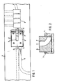
- FIG. 1 shows a plan view of a section of a waveguide arrangement 1 which has, for example, a multi-circuit filter 2 and a directional coupler 3.
- a measuring point should be provided between the filter 2 and the directional coupler 3.
- an opening 5 is milled into the accessible upper side wall of the waveguide 4 extending between the filter 2 and the directional coupler 3, which opening is normally closed by a removable cover.
- this cover is removed and a coupling device is inserted into the opening 5 in its place.
- the coupling device serves to either couple a measurement signal into the waveguide 4 in order to couple it out again at another point in the waveguide arrangement for the measurement or to couple out a measurement signal coupled in somewhere else for measurement purposes. Three possible embodiments for such a coupling device will now be described.
- the coupling element shown in FIG. 1 as a top view and in longitudinal section AA in FIG. 2 is a deflection element 6 in the form of a waveguide piece 7 which is curved in the H plane (or E plane) and penetrates into the waveguide 4 without contact. Via this curved waveguide piece 7, either measurement signals of a certain direction of propagation are led out of the waveguide 4 to an input or output port 8 of the deflecting element 6 or measurement signals which are fed into the input or output port 8 are introduced into the waveguide 4.
- the direction in which measurement signals are coupled or from which measurement signals are coupled depends on the direction of curvature of the waveguide section 7. The direction can be reversed by simply turning the deflecting element 6.
- a blocking structure (waffle iron structure) embedded in the end of the curved waveguide section 7 projecting into the waveguide 4 prevents wave propagation through the gap between the deflection element 6 and the waveguide 4.
- FIG. 3 top view
- FIG. 4 longitudinal section B-B
- the deflection element 9 differs from the deflection element 6 just described in that instead of a curved waveguide piece, only a curved shaped part 10 projects into the waveguide 4 without contact. Measuring signals are guided out of the waveguide 4 to the input or output port 11 of this deflecting element 9 via the curved upper side of the molded part 10, or measuring signals are fed into it from the input or output port 11.
- the coupling or decoupling direction can be reversed by reversing the deflection element 9.
- a wave barrier structure 12 e.g. in the form of a waffle iron structure, milled. This wave barrier structure 12 prevents waves from spreading in the gaps between the molded part 10 and the waveguide inner walls.
- the coupling element 13 shown in FIG. 5 (top view) and FIG. 6 (longitudinal section CC) has the properties of a directional coupler.
- the coupling element 13 inserted into the opening 5 of the waveguide 4 has a waveguide section 14 with two input and output gates 15 and 16, which runs parallel to the waveguide 4 over a certain length and whose wall with coupling openings 17 separating it from the waveguide 4 is provided.
- the length over which the waveguide section 14 runs parallel to the waveguide 4, and the locations of the coupling openings 17 are selected such that the waveguide section 14 forms a directional coupler together with the waveguide 4.
- Such a directional coupler allows 4 measuring signals to be coupled in or out in any direction of the waveguide. If necessary, that input or output gate 15 or 16, which is not provided for the coupling or decoupling of measurement signals, can be combined with a Absorber 18 to be completed.
- the spread of measurement signals in an undesired direction in the waveguide 4 can be prevented by attaching an absorber 19 projecting into the waveguide 4 to the underside of the coupling element 13.
- an absorber 19 projecting into the waveguide 4 to the underside of the coupling element 13.
- This cover which is equipped with coupling elements, can be used for measuring any integrated waveguide circuit that is suitable for it.
Landscapes
- Physics & Mathematics (AREA)
- General Physics & Mathematics (AREA)
- Waveguide Connection Structure (AREA)
- Control Of Motors That Do Not Use Commutators (AREA)
Applications Claiming Priority (2)
| Application Number | Priority Date | Filing Date | Title |
|---|---|---|---|
| DE3832187 | 1988-09-22 | ||
| DE3832187 | 1988-09-22 |
Publications (3)
| Publication Number | Publication Date |
|---|---|
| EP0359937A2 true EP0359937A2 (fr) | 1990-03-28 |
| EP0359937A3 EP0359937A3 (en) | 1990-12-12 |
| EP0359937B1 EP0359937B1 (fr) | 1994-02-09 |
Family
ID=6363479
Family Applications (1)
| Application Number | Title | Priority Date | Filing Date |
|---|---|---|---|
| EP89113409A Expired - Lifetime EP0359937B1 (fr) | 1988-09-22 | 1989-07-21 | Dispositif d'accès d'un signal de mesure à un conducteur creux |
Country Status (3)
| Country | Link |
|---|---|
| US (1) | US4982172A (fr) |
| EP (1) | EP0359937B1 (fr) |
| DE (1) | DE58906933D1 (fr) |
Cited By (2)
| Publication number | Priority date | Publication date | Assignee | Title |
|---|---|---|---|---|
| EP0678749A3 (fr) * | 1994-04-19 | 1996-02-07 | Hirose Electric Co Ltd | Commutateur haute fréquence et procédé de test de dispositifs à hautes-fréquences. |
| US5625177A (en) * | 1995-03-03 | 1997-04-29 | Hirose Electric Co., Ltd. | High frequency switch and method of testing H-F apparatus |
Families Citing this family (1)
| Publication number | Priority date | Publication date | Assignee | Title |
|---|---|---|---|---|
| KR20050055204A (ko) * | 2003-12-05 | 2005-06-13 | 한국전자통신연구원 | 도파관 연결 장치 |
Family Cites Families (9)
| Publication number | Priority date | Publication date | Assignee | Title |
|---|---|---|---|---|
| US1517677A (en) * | 1922-11-25 | 1924-12-02 | Heinkel John | Repair-cover outfit for test tees or cleanout tees |
| DE835774C (de) * | 1948-10-02 | 1952-04-03 | Siemens & Halske A G | Einrichtung zum Messen elektrischer oder magnetischer Felder im Innern von als Messleitung dienenden konzentrischen Leitern oder Hohlleitern |
| US2820201A (en) * | 1951-02-28 | 1958-01-14 | Sperry Rand Corp | Selective transfer device for microwave energy |
| US3451432A (en) * | 1967-03-02 | 1969-06-24 | Daniel R Miller | Test plug means for fluid conduits |
| US3550637A (en) * | 1968-06-10 | 1970-12-29 | Pfaff & Kendall | Handhole access assembly |
| US3605041A (en) * | 1969-12-31 | 1971-09-14 | Bell Telephone Labor Inc | Permanent waveguide connection for occasional use |
| US4211911A (en) * | 1979-01-16 | 1980-07-08 | General Electric Company | Microwave directional coupler and detector module |
| FR2490408A1 (fr) * | 1980-09-12 | 1982-03-19 | Etude Radant Sarl | Coupleurs directifs en hyperfrequence entre guide d'onde rectangulaire et ligne triplaque |
| US4801903A (en) * | 1986-09-08 | 1989-01-31 | Varian Associates, Inc. | Waveguide loop directional coupler |
-
1989
- 1989-07-21 EP EP89113409A patent/EP0359937B1/fr not_active Expired - Lifetime
- 1989-07-21 DE DE89113409T patent/DE58906933D1/de not_active Expired - Fee Related
- 1989-09-22 US US07/410,868 patent/US4982172A/en not_active Expired - Fee Related
Cited By (2)
| Publication number | Priority date | Publication date | Assignee | Title |
|---|---|---|---|---|
| EP0678749A3 (fr) * | 1994-04-19 | 1996-02-07 | Hirose Electric Co Ltd | Commutateur haute fréquence et procédé de test de dispositifs à hautes-fréquences. |
| US5625177A (en) * | 1995-03-03 | 1997-04-29 | Hirose Electric Co., Ltd. | High frequency switch and method of testing H-F apparatus |
Also Published As
| Publication number | Publication date |
|---|---|
| DE58906933D1 (de) | 1994-03-24 |
| US4982172A (en) | 1991-01-01 |
| EP0359937A3 (en) | 1990-12-12 |
| EP0359937B1 (fr) | 1994-02-09 |
Similar Documents
| Publication | Publication Date | Title |
|---|---|---|
| DE2162196C3 (de) | Wellentypwandler | |
| DE3884115T2 (de) | Verfahren und Anordnung zur Abschätzung der elektromagnetischen Eigenschaften eines dielektrischen oder magnetischen Werkstoffes. | |
| EP0142119B1 (fr) | Dispositif pour adapter le pas d'une grille de contact d'un appareil de contrôle de circuits imprimés | |
| DE4124103C1 (fr) | ||
| DE2724939B2 (de) | Schaltgerät, insbesondere elektronisches, berührungslos arbeitendes Schaltgerät | |
| EP0278073B1 (fr) | Sonde pour un adaptateur pour un dispositif d'essai de cartes imprimées | |
| DE4241635C2 (de) | Übergang von einer Microstrip-Leitung auf einen Hohlleiter | |
| EP0359937B1 (fr) | Dispositif d'accès d'un signal de mesure à un conducteur creux | |
| WO1990000316A1 (fr) | Ensemble de commutateurs a micro-ondes | |
| DE2707231C3 (de) | Halter für Küvetten | |
| DE2828541C2 (de) | Vorrichtung zur Schwingungsmessung | |
| DE2723579C3 (de) | Vorrichtung zum Formen von Kanalisationsschächten | |
| DE19637049A1 (de) | Freiluftdurchführungen für einen Schaltfeldcontainer | |
| DE2048454B2 (de) | In ein Gehäuse eingebautes elektrisches Bauelement | |
| DE2010896C3 (de) | Bauelement, insbesondere Spielzeug- und Hochbaubauelement | |
| DE4225148A1 (de) | Elektrisches Gerät, insbesondere Klemmenkasten | |
| DE1481041A1 (de) | Vorrichtung zur Handhabung von geschuettet vorliegenden Gegenstaenden | |
| DE967797C (de) | Anordnung zur Erzielung einer einstellbaren Kopplung zwischen Hochfrequenzanordnungen, insbesondere Hochfrequenzleitungen | |
| DE2932079A1 (de) | Anordnung zum umruehren nichterstarrter schmelze in einem giesstrang | |
| EP0798804A2 (fr) | Dispositif de couplage d'une sonde à un guide d'ondes | |
| DE3150672C2 (de) | Anordnung zum Positionieren einer Grundplatte auf einer Arbeitsplatte | |
| DE1187297B (de) | Schutzgehaeuse fuer den Aufbau von gekapselten Schaltanlagen | |
| CH377900A (de) | Gehäuse, insbesondere für elektrische Apparate | |
| DE2226515A1 (de) | Gehaeuse fuer einen mikrowellenzirkulator | |
| DE3715286A1 (de) | Vorrichtung zum koppeln zweier hohlleiterbauelemente |
Legal Events
| Date | Code | Title | Description |
|---|---|---|---|
| PUAI | Public reference made under article 153(3) epc to a published international application that has entered the european phase |
Free format text: ORIGINAL CODE: 0009012 |
|
| AK | Designated contracting states |
Kind code of ref document: A2 Designated state(s): DE FR GB IT SE |
|
| PUAL | Search report despatched |
Free format text: ORIGINAL CODE: 0009013 |
|
| AK | Designated contracting states |
Kind code of ref document: A3 Designated state(s): DE FR GB IT SE |
|
| RHK1 | Main classification (correction) |
Ipc: H01P 5/00 |
|
| 17P | Request for examination filed |
Effective date: 19901102 |
|
| 17Q | First examination report despatched |
Effective date: 19930517 |
|
| GRAA | (expected) grant |
Free format text: ORIGINAL CODE: 0009210 |
|
| ITF | It: translation for a ep patent filed | ||
| AK | Designated contracting states |
Kind code of ref document: B1 Designated state(s): DE FR GB IT SE |
|
| GBT | Gb: translation of ep patent filed (gb section 77(6)(a)/1977) |
Effective date: 19940208 |
|
| REG | Reference to a national code |
Ref country code: GB Ref legal event code: 746 Effective date: 19940301 |
|
| REF | Corresponds to: |
Ref document number: 58906933 Country of ref document: DE Date of ref document: 19940324 |
|
| ET | Fr: translation filed | ||
| REG | Reference to a national code |
Ref country code: FR Ref legal event code: DL |
|
| PLBE | No opposition filed within time limit |
Free format text: ORIGINAL CODE: 0009261 |
|
| STAA | Information on the status of an ep patent application or granted ep patent |
Free format text: STATUS: NO OPPOSITION FILED WITHIN TIME LIMIT |
|
| EAL | Se: european patent in force in sweden |
Ref document number: 89113409.0 |
|
| 26N | No opposition filed | ||
| PGFP | Annual fee paid to national office [announced via postgrant information from national office to epo] |
Ref country code: GB Payment date: 19950628 Year of fee payment: 7 |
|
| PGFP | Annual fee paid to national office [announced via postgrant information from national office to epo] |
Ref country code: SE Payment date: 19950725 Year of fee payment: 7 |
|
| PG25 | Lapsed in a contracting state [announced via postgrant information from national office to epo] |
Ref country code: GB Effective date: 19960721 |
|
| PG25 | Lapsed in a contracting state [announced via postgrant information from national office to epo] |
Ref country code: SE Effective date: 19960722 |
|
| GBPC | Gb: european patent ceased through non-payment of renewal fee |
Effective date: 19960721 |
|
| EUG | Se: european patent has lapsed |
Ref document number: 89113409.0 |
|
| PGFP | Annual fee paid to national office [announced via postgrant information from national office to epo] |
Ref country code: FR Payment date: 20010712 Year of fee payment: 13 |
|
| PGFP | Annual fee paid to national office [announced via postgrant information from national office to epo] |
Ref country code: DE Payment date: 20010716 Year of fee payment: 13 |
|
| PG25 | Lapsed in a contracting state [announced via postgrant information from national office to epo] |
Ref country code: DE Free format text: LAPSE BECAUSE OF NON-PAYMENT OF DUE FEES Effective date: 20030201 |
|
| PG25 | Lapsed in a contracting state [announced via postgrant information from national office to epo] |
Ref country code: FR Free format text: LAPSE BECAUSE OF NON-PAYMENT OF DUE FEES Effective date: 20030331 |
|
| REG | Reference to a national code |
Ref country code: FR Ref legal event code: ST |
|
| PG25 | Lapsed in a contracting state [announced via postgrant information from national office to epo] |
Ref country code: IT Free format text: LAPSE BECAUSE OF NON-PAYMENT OF DUE FEES;WARNING: LAPSES OF ITALIAN PATENTS WITH EFFECTIVE DATE BEFORE 2007 MAY HAVE OCCURRED AT ANY TIME BEFORE 2007. THE CORRECT EFFECTIVE DATE MAY BE DIFFERENT FROM THE ONE RECORDED. Effective date: 20050721 |