EP0360036B1 - Jonction pn plane à tenue en tension élévée - Google Patents
Jonction pn plane à tenue en tension élévée Download PDFInfo
- Publication number
- EP0360036B1 EP0360036B1 EP89115841A EP89115841A EP0360036B1 EP 0360036 B1 EP0360036 B1 EP 0360036B1 EP 89115841 A EP89115841 A EP 89115841A EP 89115841 A EP89115841 A EP 89115841A EP 0360036 B1 EP0360036 B1 EP 0360036B1
- Authority
- EP
- European Patent Office
- Prior art keywords
- field
- semiconductor
- region
- plate
- junction
- Prior art date
- Legal status (The legal status is an assumption and is not a legal conclusion. Google has not performed a legal analysis and makes no representation as to the accuracy of the status listed.)
- Expired - Lifetime
Links
- 239000004065 semiconductor Substances 0.000 claims description 76
- 230000002093 peripheral effect Effects 0.000 claims 2
- 230000015556 catabolic process Effects 0.000 description 11
- PZASAAIJIFDWSB-CKPDSHCKSA-N 8-[(1S)-1-[8-(trifluoromethyl)-7-[4-(trifluoromethyl)cyclohexyl]oxynaphthalen-2-yl]ethyl]-8-azabicyclo[3.2.1]octane-3-carboxylic acid Chemical compound FC(F)(F)C=1C2=CC([C@@H](N3C4CCC3CC(C4)C(O)=O)C)=CC=C2C=CC=1OC1CCC(C(F)(F)F)CC1 PZASAAIJIFDWSB-CKPDSHCKSA-N 0.000 description 2
- 238000002161 passivation Methods 0.000 description 2
- 229910052710 silicon Inorganic materials 0.000 description 2
- 239000010703 silicon Substances 0.000 description 2
- 229910021417 amorphous silicon Inorganic materials 0.000 description 1
- 238000013459 approach Methods 0.000 description 1
- 230000000903 blocking effect Effects 0.000 description 1
- 239000004020 conductor Substances 0.000 description 1
- 238000011161 development Methods 0.000 description 1
- 230000018109 developmental process Effects 0.000 description 1
- 230000000694 effects Effects 0.000 description 1
- 238000005530 etching Methods 0.000 description 1
- 238000004519 manufacturing process Methods 0.000 description 1
- 239000000463 material Substances 0.000 description 1
- 238000000034 method Methods 0.000 description 1
- 230000035515 penetration Effects 0.000 description 1
- 229910021420 polycrystalline silicon Inorganic materials 0.000 description 1
- 230000007704 transition Effects 0.000 description 1
- 235000012431 wafers Nutrition 0.000 description 1
- XLYOFNOQVPJJNP-UHFFFAOYSA-N water Substances O XLYOFNOQVPJJNP-UHFFFAOYSA-N 0.000 description 1
Images

Classifications
-
- H—ELECTRICITY
- H10—SEMICONDUCTOR DEVICES; ELECTRIC SOLID-STATE DEVICES NOT OTHERWISE PROVIDED FOR
- H10D—INORGANIC ELECTRIC SEMICONDUCTOR DEVICES
- H10D64/00—Electrodes of devices having potential barriers
- H10D64/111—Field plates
- H10D64/112—Field plates comprising multiple field plate segments
-
- H—ELECTRICITY
- H10—SEMICONDUCTOR DEVICES; ELECTRIC SOLID-STATE DEVICES NOT OTHERWISE PROVIDED FOR
- H10D—INORGANIC ELECTRIC SEMICONDUCTOR DEVICES
- H10D62/00—Semiconductor bodies, or regions thereof, of devices having potential barriers
- H10D62/10—Shapes, relative sizes or dispositions of the regions of the semiconductor bodies; Shapes of the semiconductor bodies
- H10D62/102—Constructional design considerations for preventing surface leakage or controlling electric field concentration
- H10D62/103—Constructional design considerations for preventing surface leakage or controlling electric field concentration for increasing or controlling the breakdown voltage of reverse-biased devices
- H10D62/105—Constructional design considerations for preventing surface leakage or controlling electric field concentration for increasing or controlling the breakdown voltage of reverse-biased devices by having particular doping profiles, shapes or arrangements of PN junctions; by having supplementary regions, e.g. junction termination extension [JTE]
Definitions
- the invention relates to a planar pn junction of high dielectric strength according to the preamble of claim 1.
- a planar pn junction of this kind is from Jap. Journal of Appl. Physics, Vol. 21 (1982) Suppl. 21-1, pp. 97-101.
- the field plates contact the semiconductor body in the immediate vicinity of their inner edges, ie, edges facing the semiconductor region.
- the semiconductor body is additionally provided with a number of field rings corresponding to the number of field plates, which consist of annular semiconductor zones which have the same conductivity type as the semiconductor region delimited by the pn junction.
- the field rings surround the semiconductor region at an increasing distance from the edge of the pn junction.
- Each one of the field plates contacts a field ring assigned to it, so that it determines the potential of the field plate.
- the field plates cause the pn junction to have a high breakdown voltage in its planar edge region when a voltage blocking it, which is supplied via two electrodes contacting the semiconductor region and the semiconductor body, is applied.
- This breakdown voltage corresponds approximately to its volume breakdown voltage, which is defined as the voltage at which the pn junction breaks down in its part running parallel to the interface of the semiconductor body, that is to say in the volume of the semiconductor body.
- the invention is based on the object of specifying a planar pn junction of the type mentioned at the outset which can be implemented for a desired high breakdown voltage on a substantially smaller semiconductor area than is the case with the known pn junction. This is achieved according to the invention by training according to the characterizing part of patent claim 1.
- the advantage that can be achieved with the invention is, in particular, that the pn junction can be implemented on a relatively small semiconductor area, but a high breakdown voltage value is achieved for its planar edge region, which corresponds approximately to the volume breakdown voltage. Furthermore, the value of the breakdown voltage in the edge region is independent of the value of the doping concentration of the semiconductor body, since the field plates each cover parts of the semiconductor zone that extend the semiconductor region in the lateral direction and have the same conductivity type as the semiconductor region. In contrast to this, the field plates of the above-mentioned known pn junction cover sub-zones of the semiconductor body which are weakly doped and have a conductivity type opposite to the semiconductor region.
- Claims 2 and 3 are directed to preferred refinements and developments of the invention.
- a semiconductor body 1 e.g. made of n-doped silicon with a doping concentration of 1014cm ⁇ 3, in which a p-type semiconductor region 2 is inserted.
- this has a doping concentration of 1018cm ⁇ 3.
- the semiconductor region 2 is extended in the lateral direction by a p-doped semiconductor zone 3, the degree of doping of which is e.g. 1016cm ⁇ 3 and is therefore significantly lower than that of the semiconductor region 2.
- the semiconductor region 2 and the semiconductor zone 3 are separated from the rest of the semiconductor body 1 by a pn junction 4a, 4b.
- the part 4a of the pn junction runs essentially parallel to the interface 1a of the semiconductor body 1, the part 4b gradually approaches the interface 1a with increasing distance from the edge of the semiconductor region 2 and reaches it at 5.
- the semiconductor zone 3 can expediently be produced by a method which is described in detail in EP-A-0 176 778. Another method for producing this semiconductor zone can be found in IEEE Transactions on Electron Devices, ED-30 (1983), p. 954.
- an electrically insulating layer 10 is applied to the interface 1a, which e.g. has a layer thickness of 10 microns.
- Field plates 11 to 15 made of electrically conductive material, e.g. Al or highly doped polycrystalline silicon, of which the innermost field plate, designated 11, lies directly in the edge region of the semiconductor region 2 and contacts it with its inner plate edge 11a.
- the field plates 12, 13, 14 and 15 have increasing distances from the semiconductor region 2 in this order, the outermost field plate 15 contacting the semiconductor body 1 outside the edge 5 of the pn junction 4a, 4b with its right, ie outer, plate edge 15a.
- An n-type contact zone 16 is expediently inserted into the semiconductor body 1, which e.g.
- the field plate 15 then contacts the contact zone 16.
- the field plates 12, 13 and 14 contact the p-type semiconductor zone 3 in the area of contact holes 17, 18 and 19, respectively.
- the contact hole 17 is arranged such that there are equal distances from the inner plate edge 12a and from the outer plate edge 12b of the field plate 12.
- the contact holes 18 and 19 are also arranged such that they are each at the same distances from the inner and outer edges of the field plates 13 and 14 assigned to them.
- the field plates 11 to 15 are each arranged so close to one another that they only leave narrow gaps between them, e.g. Amount to 10 ⁇ m.
- the entire field plate arrangement 11 to 15 can be covered by an insulating layer 20, which serves for passivation. It consists, for example, of amorphous silicon or rubber.
- the dashed lines 23 to 29 located between 21 and 22 then each represent further equipotential lines for intermediate voltage values graded with respect to one another, whereby 23 denotes, for example, a potential value which differs only slightly from U, while the points on line 29 differ only slightly have potential differentiating from ground potential.
- the equipotential lines 29 and 28 run, as shown in FIG. 1, through the gap between the field plates 11 and 12, the equipotential lines 27 and 26 through the gap between 12 and 13, and so on.
- the semiconductor zone 3 below the part of the field plate 12 which extends from the contact hole 17 to the left plate edge 12a is provided with a local doping maximum, which is indicated by a hatched area 30.
- the course of the equipotential line 26 is straightened in an analogous manner by a further local doping maximum 31 of the semiconductor zone 3.
- the course of the equipotential lines 21 to 29 shows that even with large values of U at the interface 1a in areas of the pn junction 4b which lie between the contact holes, for example 17, and the left field plate edges, for example 12a, the field gradients do not exist become so large that there is a risk of breakdown in the silicon.
- the structure according to the invention is characterized in that the lateral voltage drop in the area between the interface 1a and the pn junction 4b is uniform and accordingly there is also a relatively uniform field distribution within the space charge zone 21, 22 in the vicinity of the interface 1a, even though the left from the associated contact holes, for example 17, arranged Field plate edges, eg 12a, would cause disturbances in the uniform field course.
- the lateral maxima of the doping concentration which are present within the shaded areas 30, 31 and 32 of the semiconductor zone 3, for example, can be higher by a factor of 10 than the values of the doping concentration in the adjoining parts of the zone 3.
- the large area coverage of the edge area of the pn junction 4a, 4b through the field plates 11 to 15, which only leave narrow gaps between them, has the effect that the high breakdown voltage achievable with the structure according to the invention is not reduced even by the influence of, for example, water-containing materials which are used for passivation becomes.
- the pn structure according to FIG. 1 is also important for vertical bipolar power transistors, for example.
- Such a transistor is obtained if an n-type semiconductor region 33 is inserted into the p-semiconductor region 2 in such a way that it is separated from the latter by a further pn junction 34.
- 33 designates the emitter region, 2 and 3 the base region and 1 the collector region of the transistor.
- the electrodes 6 and 8 represent the collector and emitter electrode, 7 and 9 the collector and emitter connection.
- the base region 2 is provided with a base electrode, not shown, which has a connection for a base circuit.
- the high breakdown voltage achievable with the invention at the base-collector junction 4a, 4b brings about a high dielectric strength of this transistor.
- FIG. 2 shows the application of the pn structure according to FIG. 1 to a thyristor.
- the region 33 here represents the n-emitter, the region 2 including the zone 3 the p-base, the part of the semiconductor body 1 below 4a and 4b the n-base and an additional, p-doped semiconductor layer 35 on the underside of 1 the p-emitter of the thyristor.
- the electrode 8 means the electrode on the cathode side and an electrode 36 contacting the layer 35 means the electrode on the anode side of the thyristor.
- the connections of 8 and 36 are designated K and A here.
- An electrode (not shown) which contacts the region 2 forms the gate electrode of the thyristor, which is acted upon by ignition or extinguishing signals in order to ignite and / or to extinguish the same.
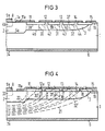
- FIG. 3 shows an alternative structural configuration of the arrangement according to FIG. 1.
- an electrically insulating layer 37 is provided here, which is grown within the semiconductor zone 3 or the semiconductor body 1 after etching out recesses 38 to 41.
- the web-shaped parts 42 to 44 of the semiconductor zone 3 remaining between the recesses 38 to 41 are contacted by the field plates 12 to 14 applied to the insulating layer 37, while the field plates 11 and 15 according to FIG. 1 contact the semiconductor region 2 and the region 16 to contact.
- the course of the equipotential lines, not shown, within the space charge zone building up at the pn junction 4a, 4b when a reverse voltage is applied corresponds to the illustration according to FIG. 1.
- the structure according to FIG. 3 is also when an n-conducting region 45 is inserted into region 2 important for bipolar transistors and, if used accordingly in FIG. 2, also for thyristors.
- Fig. 4 shows an embodiment of the invention, in which the distance of the contact holes, for example 17, from the field plate edges, for example 12a, is not constant, but varies from field plate to field plate.
- the innermost and outermost field plates 11 and 15 are formed in the same way as in Fig. 1, while the distances of the contact holes of the field plates 12 to 14 from the respective left plate edges from a relatively small value in the field plate 12 to one relatively large value increase with the field plate 14.
- the contact hole 17 is also at a clear distance from the left plate edge 12a, just like the contact hole 19 from the right plate edge of the field plate 14.
- the areas of the local doping maxima 30 ', 31' and 32 'in the p-doped semiconductor zone have different widths.
- the equipotential lines 21, 22 and the intermediate equipotential lines have approximately the same course as in FIG. 1.
- the structure according to FIG. 4 can in particular have a smaller penetration depth of the semiconductor zone 3 than the structure according to FIG. 1.
- the illustrated exemplary embodiments of the pn junction according to the invention are preferably on rotationally symmetrical semiconductor bodies, i.e. Semiconductor wafers with circular lateral boundaries, realized.
- the parts 2, 3, 33 and 45 also have circular lateral boundaries, while the field plates 11 to 15 have the shape of circular rings.
- the invention also includes those in which the semiconductor regions mentioned are in each case replaced by those of the opposite conductivity type, a voltage of the opposite sign being used instead of the voltage U mentioned.
Landscapes
- Thyristors (AREA)
- Electrodes Of Semiconductors (AREA)
- Bipolar Transistors (AREA)
Claims (3)
- Jonction pn planar (4a, 4b) à grande rigidité diélectrique, qui s'étend essentiellement parallèlement à la surface limite (1a) d'un corps semiconducteur dopé (1) d'un premier type de conductivité, et qui sépare une région semiconductrice (2), insérée dans ce corps, d'un second type de conductivité, du reste du corps semiconducteur (1), un grand nombre de magnétorésistances (11 à 15) étant prévues dans la zone marginale de la région semiconductrice (2), ces magnétorésistances étant séparées de la surface limite (1a) par une couche électriquement isolante (10) et établissant un contact avec le corps semiconducteur dans la zone d'un trou de contact (17 à 19) de cette couche (10), caractérisée par le fait qu'au moins dans une partie des magnétorésistances (12 à 14), à l'exception de la magnétorésistance la plus intérieure (11) et de la magnétorésistance la plus extérieure (15), la disposition des trous de contact (17) est telle qu'ils sont situés à une distance du bord intérieur (12a) de la magnétorésistance, qui correspond, qui est inférieure ou qui est supérieure à leur distance par rapport au bord extérieur (12b) de la magnétorésistance, le degré de dépassement par valeur inférieure ou supérieure étant juste suffisant pour que les trous de contact (17) soient encore situés à une distance nette du bord intérieur (12a) et du bord extérieur(12b) de la magnétorésistance, que la région semiconductrice (2) est prolongée, dans une direction latérale, par une zone semiconductrice (3) du second type de conductivité qui est située en-dessous des magnétorésistances (11 à 15), et qui comporte une terminaison marginale planar et dont le degré de dopage est nettement inférieur à celui de la région semiconductrice (2), et que la valeur du degré de dopage de la zone semiconductrice (3) varie dans la direction latérale, en présentant des maxima locaux (30) en-dessous des parties des magnétorésistances, qui sont situées entre les trous de contact (17) et les bords intérieurs (12a)des magnétorésistance (12) associées.
- Jonction pn planar suivant la revendication 1, caractérisée par le fait que la couche électriquement isolante (37) est constituée d'une multiplicité de couches partielles, qui sont prévues à l'intérieur d'une multiplicité d'évidements surfaciques (38 à 41) de la zone semiconductrice (3), qu'entre deux évidements (38, 39) de ce type, voisins l'un de l'autre, est prévue une barrette (42) de la zone semiconductrice (3), qui s'étend jusqu'à la surface limite (1a) et qui sert à établir le contact avec une magnétorésistance (12), qui est disposée sur les couches partielles situées dans les évidements voisins (38, 39), et que les bords, qui jouxtent la barrette (42), des couches partielles qui sont prévues dans les évidements voisins (38, 39), limitent entre eux le trou de contact associé à cette magnétorésistance (12).
- Jonction pn planar suivant la revendication 1 ou 2, caractérisé par le fait que les distances entre les trous de contact (17) et les bords intérieurs (12a) des magnétorésistances (12) qui leur sont associées, augmentent avec l'augmentation de la distance entre les magnétorésistances (12) et le bord de la région semiconductrice (2).
Applications Claiming Priority (2)
| Application Number | Priority Date | Filing Date | Title |
|---|---|---|---|
| DE3831941 | 1988-09-20 | ||
| DE3831941 | 1988-09-20 |
Publications (3)
| Publication Number | Publication Date |
|---|---|
| EP0360036A2 EP0360036A2 (fr) | 1990-03-28 |
| EP0360036A3 EP0360036A3 (en) | 1990-05-30 |
| EP0360036B1 true EP0360036B1 (fr) | 1994-06-01 |
Family
ID=6363338
Family Applications (1)
| Application Number | Title | Priority Date | Filing Date |
|---|---|---|---|
| EP89115841A Expired - Lifetime EP0360036B1 (fr) | 1988-09-20 | 1989-08-28 | Jonction pn plane à tenue en tension élévée |
Country Status (4)
| Country | Link |
|---|---|
| US (1) | US5113237A (fr) |
| EP (1) | EP0360036B1 (fr) |
| JP (1) | JP2974696B2 (fr) |
| DE (1) | DE58907758D1 (fr) |
Cited By (1)
| Publication number | Priority date | Publication date | Assignee | Title |
|---|---|---|---|---|
| DE102008032711B4 (de) | 2007-07-12 | 2019-01-03 | Fuji Electric Co., Ltd. | Halbleitervorrichtung |
Families Citing this family (39)
| Publication number | Priority date | Publication date | Assignee | Title |
|---|---|---|---|---|
| JP2850694B2 (ja) * | 1993-03-10 | 1999-01-27 | 株式会社日立製作所 | 高耐圧プレーナ型半導体装置 |
| US5959342A (en) * | 1993-12-08 | 1999-09-28 | Lucent Technologies Inc. | Semiconductor device having a high voltage termination improvement |
| US5381031A (en) * | 1993-12-22 | 1995-01-10 | At&T Corp. | Semiconductor device with reduced high voltage termination area and high breakdown voltage |
| US5486718A (en) * | 1994-07-05 | 1996-01-23 | Motorola, Inc. | High voltage planar edge termination structure and method of making same |
| JP3581447B2 (ja) * | 1995-08-22 | 2004-10-27 | 三菱電機株式会社 | 高耐圧半導体装置 |
| US5801836A (en) * | 1996-07-16 | 1998-09-01 | Abb Research Ltd. | Depletion region stopper for PN junction in silicon carbide |
| DE19843659A1 (de) * | 1998-09-23 | 2000-04-06 | Siemens Ag | Halbleiterbauelement mit strukturiertem Halbleiterkörper |
| JP2002533934A (ja) * | 1998-12-18 | 2002-10-08 | インフィネオン テクノロジース アクチエンゲゼルシャフト | 出力半導体構造素子 |
| DE10051909B4 (de) * | 2000-10-19 | 2007-03-22 | Infineon Technologies Ag | Randabschluss für Hochvolt-Halbleiterbauelement und Verfahren zum Herstellen eines Isolationstrenches in einem Halbleiterkörper für solchen Randabschluss |
| US6563197B1 (en) * | 2001-11-20 | 2003-05-13 | International Rectifier Corporation | MOSgated device termination with guard rings under field plate |
| JP4326835B2 (ja) * | 2003-05-20 | 2009-09-09 | 三菱電機株式会社 | 半導体装置、半導体装置の製造方法及び半導体装置の製造プロセス評価方法 |
| US7812441B2 (en) | 2004-10-21 | 2010-10-12 | Siliconix Technology C.V. | Schottky diode with improved surge capability |
| TWI278090B (en) * | 2004-10-21 | 2007-04-01 | Int Rectifier Corp | Solderable top metal for SiC device |
| US9419092B2 (en) * | 2005-03-04 | 2016-08-16 | Vishay-Siliconix | Termination for SiC trench devices |
| US7834376B2 (en) * | 2005-03-04 | 2010-11-16 | Siliconix Technology C. V. | Power semiconductor switch |
| US7955345B2 (en) * | 2005-04-01 | 2011-06-07 | Nexgen Medical Systems, Inc. | Thrombus removal system and process |
| US20060255401A1 (en) * | 2005-05-11 | 2006-11-16 | Yang Robert K | Increasing breakdown voltage in semiconductor devices with vertical series capacitive structures |
| DE102005023668B3 (de) * | 2005-05-23 | 2006-11-09 | Infineon Technologies Ag | Halbleiterbauelement mit einer Randstruktur mit Spannungsdurchbruch im linearen Bereich |
| US7550787B2 (en) * | 2005-05-31 | 2009-06-23 | International Business Machines Corporation | Varied impurity profile region formation for varying breakdown voltage of devices |
| US20070012983A1 (en) * | 2005-07-15 | 2007-01-18 | Yang Robert K | Terminations for semiconductor devices with floating vertical series capacitive structures |
| US8368165B2 (en) * | 2005-10-20 | 2013-02-05 | Siliconix Technology C. V. | Silicon carbide Schottky diode |
| KR101193453B1 (ko) * | 2006-07-31 | 2012-10-24 | 비쉐이-실리코닉스 | 실리콘 카바이드 쇼트키 다이오드를 위한 몰리브덴 장벽 금속 및 제조방법 |
| US20090189240A1 (en) * | 2008-01-25 | 2009-07-30 | Infineon Technologies Austria Ag | Semiconductor device with at least one field plate |
| CN101414634B (zh) * | 2008-12-01 | 2010-06-02 | 西安电子科技大学 | 凹槽绝缘栅型复合源场板的异质结场效应晶体管 |
| US8084827B2 (en) | 2009-03-27 | 2011-12-27 | National Semiconductor Corporation | Structure and fabrication of like-polarity field-effect transistors having different configurations of source/drain extensions, halo pockets, and gate dielectric thicknesses |
| US7968921B2 (en) | 2009-03-27 | 2011-06-28 | National Semiconductor Corporation | Asymmetric field-effect transistor having asymmetric channel zone and differently configured source/drain extensions |
| US8410549B2 (en) * | 2009-03-27 | 2013-04-02 | National Semiconductor Corporation | Structure and fabrication of field-effect transistor using empty well in combination with source/drain extensions or/and halo pocket |
| US8163619B2 (en) * | 2009-03-27 | 2012-04-24 | National Semiconductor Corporation | Fabrication of semiconductor structure having asymmetric field-effect transistor with tailored pocket portion along source/drain zone |
| US20100244151A1 (en) * | 2009-03-27 | 2010-09-30 | National Semiconductor Corporation | Structure and fabrication of field-effect transistor having source/drain extension defined by multiple local concentration maxima |
| US7973372B2 (en) * | 2009-03-27 | 2011-07-05 | National Semiconductor Corporation | Semiconductor structure in which source and drain extensions of field-effect transistor are defined with different dopants |
| JP5515922B2 (ja) * | 2010-03-24 | 2014-06-11 | 富士電機株式会社 | 半導体装置 |
| KR101379162B1 (ko) | 2010-10-15 | 2014-03-28 | 미쓰비시덴키 가부시키가이샤 | 반도체 장치 및 그 제조 방법 |
| US9614043B2 (en) | 2012-02-09 | 2017-04-04 | Vishay-Siliconix | MOSFET termination trench |
| US9842911B2 (en) | 2012-05-30 | 2017-12-12 | Vishay-Siliconix | Adaptive charge balanced edge termination |
| JP6020317B2 (ja) | 2013-04-05 | 2016-11-02 | 三菱電機株式会社 | 半導体素子 |
| JP2014204038A (ja) * | 2013-04-08 | 2014-10-27 | 三菱電機株式会社 | 半導体装置及びその製造方法 |
| US9887259B2 (en) | 2014-06-23 | 2018-02-06 | Vishay-Siliconix | Modulated super junction power MOSFET devices |
| KR102098996B1 (ko) | 2014-08-19 | 2020-04-08 | 비쉐이-실리코닉스 | 초접합 금속 산화물 반도체 전계 효과 트랜지스터 |
| DE102016120301A1 (de) * | 2016-10-25 | 2018-04-26 | Infineon Technologies Ag | Leistungshalbleitervorrichtungs-Abschlussstruktur |
Family Cites Families (22)
| Publication number | Priority date | Publication date | Assignee | Title |
|---|---|---|---|---|
| NL6904619A (fr) * | 1969-03-25 | 1970-09-29 | ||
| DE1920397A1 (de) * | 1969-04-22 | 1970-11-12 | Siemens Ag | Stabilisiertes Halbleiterbauelement |
| DE2241600A1 (de) * | 1971-08-26 | 1973-03-01 | Dionics Inc | Hochspannungs-p-n-uebergang und seine anwendung in halbleiterschaltelementen, sowie verfahren zu seiner herstellung |
| JPS523277B2 (fr) * | 1973-05-19 | 1977-01-27 | ||
| US4079403A (en) * | 1976-11-01 | 1978-03-14 | Electric Power Research Institute, Inc. | Thyristor device with self-protection against breakover turn-on failure |
| DE2846637A1 (de) * | 1978-10-11 | 1980-04-30 | Bbc Brown Boveri & Cie | Halbleiterbauelement mit mindestens einem planaren pn-uebergang und zonen- guard-ringen |
| DE3117804A1 (de) * | 1981-05-06 | 1982-11-25 | Robert Bosch Gmbh, 7000 Stuttgart | "planare transistorstruktur" |
| DE3201545A1 (de) * | 1982-01-20 | 1983-07-28 | Robert Bosch Gmbh, 7000 Stuttgart | Planare halbleiteranordnung |
| JPS5976466A (ja) * | 1982-10-25 | 1984-05-01 | Mitsubishi Electric Corp | プレ−ナ形半導体装置 |
| NL8204105A (nl) * | 1982-10-25 | 1984-05-16 | Philips Nv | Halfgeleiderinrichting. |
| GB2131603B (en) * | 1982-12-03 | 1985-12-18 | Philips Electronic Associated | Semiconductor devices |
| GB2134705B (en) * | 1983-01-28 | 1985-12-24 | Philips Electronic Associated | Semiconductor devices |
| JPS60124865A (ja) * | 1983-12-09 | 1985-07-03 | Nec Corp | 半導体装置 |
| NL8401983A (nl) * | 1984-06-22 | 1986-01-16 | Philips Nv | Halfgeleiderinrichting met verhoogde doorslagspanning. |
| DE3581348D1 (de) * | 1984-09-28 | 1991-02-21 | Siemens Ag | Verfahren zum herstellen eines pn-uebergangs mit hoher durchbruchsspannung. |
| GB2167229B (en) * | 1984-11-21 | 1988-07-20 | Philips Electronic Associated | Semiconductor devices |
| JPS61135158A (ja) * | 1984-12-06 | 1986-06-23 | Nec Corp | 高耐圧半導体装置 |
| IT1202311B (it) * | 1985-12-11 | 1989-02-02 | Sgs Microelettronica Spa | Dispositivo a semiconduttore con una giunzione piana a terminazione auto passivante |
| US4799100A (en) * | 1987-02-17 | 1989-01-17 | Siliconix Incorporated | Method and apparatus for increasing breakdown of a planar junction |
| GB2205682A (en) * | 1987-06-03 | 1988-12-14 | Philips Electronic Associated | A semiconductor device |
| EP0310836A3 (fr) * | 1987-10-08 | 1989-06-14 | Siemens Aktiengesellschaft | Elément semi-conducteur avec une jonction pn planaire |
| US4903086A (en) * | 1988-01-19 | 1990-02-20 | E-Systems, Inc. | Varactor tuning diode with inversion layer |
-
1989
- 1989-08-28 EP EP89115841A patent/EP0360036B1/fr not_active Expired - Lifetime
- 1989-08-28 DE DE58907758T patent/DE58907758D1/de not_active Expired - Fee Related
- 1989-09-13 JP JP1239750A patent/JP2974696B2/ja not_active Expired - Fee Related
-
1991
- 1991-05-06 US US07/698,332 patent/US5113237A/en not_active Expired - Lifetime
Cited By (1)
| Publication number | Priority date | Publication date | Assignee | Title |
|---|---|---|---|---|
| DE102008032711B4 (de) | 2007-07-12 | 2019-01-03 | Fuji Electric Co., Ltd. | Halbleitervorrichtung |
Also Published As
| Publication number | Publication date |
|---|---|
| DE58907758D1 (de) | 1994-07-07 |
| EP0360036A3 (en) | 1990-05-30 |
| EP0360036A2 (fr) | 1990-03-28 |
| JP2974696B2 (ja) | 1999-11-10 |
| US5113237A (en) | 1992-05-12 |
| JPH02114646A (ja) | 1990-04-26 |
Similar Documents
| Publication | Publication Date | Title |
|---|---|---|
| EP0360036A2 (fr) | Jonction pn plane à tenue en tension élévée | |
| DE69305909T2 (de) | Leistungsanordnung mit isoliertem Gate-Kontakt-Gebiet | |
| EP0200863B1 (fr) | Dispositif à semi-conducteur comportant des structures de type thyristor et diode | |
| DE19701189B4 (de) | Halbleiterbauteil | |
| DE112019003790T5 (de) | Superjunction-siliziumkarbid-halbleitervorrichtung und verfahren zum herstellen einer superjunction-siliziumkarbid-halbleitervorrichtung | |
| CH638928A5 (de) | Halbleiteranordnung. | |
| DE19813509A1 (de) | Thyristor mit isoliertem Gate | |
| DE19811297A1 (de) | MOS-Halbleitervorrichtung mit hoher Durchbruchspannung | |
| EP0913000B1 (fr) | Composant a semiconducteur pouvant etre commande par effet de champ | |
| DE19816448C1 (de) | Universal-Halbleiterscheibe für Hochspannungs-Halbleiterbauelemente, ihr Herstellungsverfahren und ihre Verwendung | |
| EP0477594B1 (fr) | Thyristor à passage à l'ouverture | |
| DE3723150C2 (fr) | ||
| DE69122902T2 (de) | Halbleiteranordnung mit einem Thyristor | |
| EP0710988B1 (fr) | Procédé pour la fabrication des dispositifs semiconducteurs controlables par effet de champ | |
| DE102016120301A1 (de) | Leistungshalbleitervorrichtungs-Abschlussstruktur | |
| DE4310606C2 (de) | GTO-Thyristoren | |
| EP0332955A2 (fr) | Thyristor ayant une forte capacité de blocage direct et inverse et méthode de fabrication correpondante | |
| EP0249122B1 (fr) | Dispositif semi-conducteur de puissance pouvant être mis hors circuit | |
| DE2329398C3 (de) | In Rückwärtsrichtung leitendes Thyristorbauelement | |
| EP0419898B1 (fr) | Méthode pour augmenter la tenue en tension d'un dispositif semi-conducteur à plusieurs couches | |
| EP0768717A2 (fr) | Dispositif semi-conducteur de puissance | |
| DE69232679T2 (de) | Halbleiterbauelement für hohe Durchbruchsspannungen | |
| DE102004005084B4 (de) | Halbleiterbauelement | |
| DE2425364A1 (de) | Gate-gesteuerter halbleitergleichrichter | |
| EP0285923B1 (fr) | Thyristor à commande d'extinction et méthode de fabrication |
Legal Events
| Date | Code | Title | Description |
|---|---|---|---|
| PUAI | Public reference made under article 153(3) epc to a published international application that has entered the european phase |
Free format text: ORIGINAL CODE: 0009012 |
|
| AK | Designated contracting states |
Kind code of ref document: A2 Designated state(s): CH DE GB LI SE |
|
| PUAL | Search report despatched |
Free format text: ORIGINAL CODE: 0009013 |
|
| AK | Designated contracting states |
Kind code of ref document: A3 Designated state(s): CH DE GB LI SE |
|
| 17P | Request for examination filed |
Effective date: 19901127 |
|
| 17Q | First examination report despatched |
Effective date: 19930806 |
|
| GRAA | (expected) grant |
Free format text: ORIGINAL CODE: 0009210 |
|
| AK | Designated contracting states |
Kind code of ref document: B1 Designated state(s): CH DE GB LI SE |
|
| REF | Corresponds to: |
Ref document number: 58907758 Country of ref document: DE Date of ref document: 19940707 |
|
| GBT | Gb: translation of ep patent filed (gb section 77(6)(a)/1977) |
Effective date: 19940811 |
|
| EAL | Se: european patent in force in sweden |
Ref document number: 89115841.2 |
|
| PLBE | No opposition filed within time limit |
Free format text: ORIGINAL CODE: 0009261 |
|
| STAA | Information on the status of an ep patent application or granted ep patent |
Free format text: STATUS: NO OPPOSITION FILED WITHIN TIME LIMIT |
|
| 26N | No opposition filed | ||
| PGFP | Annual fee paid to national office [announced via postgrant information from national office to epo] |
Ref country code: SE Payment date: 20010829 Year of fee payment: 13 |
|
| PGFP | Annual fee paid to national office [announced via postgrant information from national office to epo] |
Ref country code: CH Payment date: 20011112 Year of fee payment: 13 |
|
| REG | Reference to a national code |
Ref country code: GB Ref legal event code: IF02 |
|
| PG25 | Lapsed in a contracting state [announced via postgrant information from national office to epo] |
Ref country code: SE Free format text: LAPSE BECAUSE OF NON-PAYMENT OF DUE FEES Effective date: 20020829 |
|
| PG25 | Lapsed in a contracting state [announced via postgrant information from national office to epo] |
Ref country code: CH Free format text: LAPSE BECAUSE OF NON-PAYMENT OF DUE FEES Effective date: 20020831 Ref country code: LI Free format text: LAPSE BECAUSE OF NON-PAYMENT OF DUE FEES Effective date: 20020831 |
|
| EUG | Se: european patent has lapsed | ||
| REG | Reference to a national code |
Ref country code: CH Ref legal event code: PL |
|
| PGFP | Annual fee paid to national office [announced via postgrant information from national office to epo] |
Ref country code: GB Payment date: 20050816 Year of fee payment: 17 |
|
| GBPC | Gb: european patent ceased through non-payment of renewal fee |
Effective date: 20060828 |
|
| PG25 | Lapsed in a contracting state [announced via postgrant information from national office to epo] |
Ref country code: GB Free format text: LAPSE BECAUSE OF NON-PAYMENT OF DUE FEES Effective date: 20060828 |
|
| PGFP | Annual fee paid to national office [announced via postgrant information from national office to epo] |
Ref country code: DE Payment date: 20071011 Year of fee payment: 19 |
|
| PG25 | Lapsed in a contracting state [announced via postgrant information from national office to epo] |
Ref country code: DE Free format text: LAPSE BECAUSE OF NON-PAYMENT OF DUE FEES Effective date: 20090303 |