EP0913000B1 - Composant a semiconducteur pouvant etre commande par effet de champ - Google Patents
Composant a semiconducteur pouvant etre commande par effet de champ Download PDFInfo
- Publication number
- EP0913000B1 EP0913000B1 EP98906848A EP98906848A EP0913000B1 EP 0913000 B1 EP0913000 B1 EP 0913000B1 EP 98906848 A EP98906848 A EP 98906848A EP 98906848 A EP98906848 A EP 98906848A EP 0913000 B1 EP0913000 B1 EP 0913000B1
- Authority
- EP
- European Patent Office
- Prior art keywords
- zone
- semiconductor body
- shielding
- base
- emitter
- Prior art date
- Legal status (The legal status is an assumption and is not a legal conclusion. Google has not performed a legal analysis and makes no representation as to the accuracy of the status listed.)
- Expired - Lifetime
Links
- 239000004065 semiconductor Substances 0.000 title claims description 33
- 230000005669 field effect Effects 0.000 title description 4
- 239000002800 charge carrier Substances 0.000 description 6
- 238000005516 engineering process Methods 0.000 description 4
- 230000000903 blocking effect Effects 0.000 description 3
- 239000000969 carrier Substances 0.000 description 3
- 230000015556 catabolic process Effects 0.000 description 2
- 239000002019 doping agent Substances 0.000 description 2
- 229910052751 metal Inorganic materials 0.000 description 2
- 239000002184 metal Substances 0.000 description 2
- 230000035515 penetration Effects 0.000 description 2
- 230000003068 static effect Effects 0.000 description 2
- ZOXJGFHDIHLPTG-UHFFFAOYSA-N Boron Chemical compound [B] ZOXJGFHDIHLPTG-UHFFFAOYSA-N 0.000 description 1
- 229910052782 aluminium Inorganic materials 0.000 description 1
- XAGFODPZIPBFFR-UHFFFAOYSA-N aluminium Chemical compound [Al] XAGFODPZIPBFFR-UHFFFAOYSA-N 0.000 description 1
- 238000000137 annealing Methods 0.000 description 1
- 230000005540 biological transmission Effects 0.000 description 1
- 229910052796 boron Inorganic materials 0.000 description 1
- 238000005530 etching Methods 0.000 description 1
- 238000002513 implantation Methods 0.000 description 1
- 238000004519 manufacturing process Methods 0.000 description 1
- 238000001465 metallisation Methods 0.000 description 1
- 238000012856 packing Methods 0.000 description 1
- 229910021420 polycrystalline silicon Inorganic materials 0.000 description 1
- 229920005591 polysilicon Polymers 0.000 description 1
- 239000000758 substrate Substances 0.000 description 1
Images

Classifications
-
- H—ELECTRICITY
- H10—SEMICONDUCTOR DEVICES; ELECTRIC SOLID-STATE DEVICES NOT OTHERWISE PROVIDED FOR
- H10D—INORGANIC ELECTRIC SEMICONDUCTOR DEVICES
- H10D12/00—Bipolar devices controlled by the field effect, e.g. insulated-gate bipolar transistors [IGBT]
-
- H—ELECTRICITY
- H10—SEMICONDUCTOR DEVICES; ELECTRIC SOLID-STATE DEVICES NOT OTHERWISE PROVIDED FOR
- H10D—INORGANIC ELECTRIC SEMICONDUCTOR DEVICES
- H10D62/00—Semiconductor bodies, or regions thereof, of devices having potential barriers
- H10D62/10—Shapes, relative sizes or dispositions of the regions of the semiconductor bodies; Shapes of the semiconductor bodies
- H10D62/13—Semiconductor regions connected to electrodes carrying current to be rectified, amplified or switched, e.g. source or drain regions
- H10D62/149—Source or drain regions of field-effect devices
- H10D62/151—Source or drain regions of field-effect devices of IGFETs
-
- H—ELECTRICITY
- H10—SEMICONDUCTOR DEVICES; ELECTRIC SOLID-STATE DEVICES NOT OTHERWISE PROVIDED FOR
- H10D—INORGANIC ELECTRIC SEMICONDUCTOR DEVICES
- H10D12/00—Bipolar devices controlled by the field effect, e.g. insulated-gate bipolar transistors [IGBT]
- H10D12/411—Insulated-gate bipolar transistors [IGBT]
- H10D12/441—Vertical IGBTs
-
- H—ELECTRICITY
- H10—SEMICONDUCTOR DEVICES; ELECTRIC SOLID-STATE DEVICES NOT OTHERWISE PROVIDED FOR
- H10D—INORGANIC ELECTRIC SEMICONDUCTOR DEVICES
- H10D62/00—Semiconductor bodies, or regions thereof, of devices having potential barriers
- H10D62/10—Shapes, relative sizes or dispositions of the regions of the semiconductor bodies; Shapes of the semiconductor bodies
- H10D62/102—Constructional design considerations for preventing surface leakage or controlling electric field concentration
- H10D62/103—Constructional design considerations for preventing surface leakage or controlling electric field concentration for increasing or controlling the breakdown voltage of reverse-biased devices
- H10D62/105—Constructional design considerations for preventing surface leakage or controlling electric field concentration for increasing or controlling the breakdown voltage of reverse-biased devices by having particular doping profiles, shapes or arrangements of PN junctions; by having supplementary regions, e.g. junction termination extension [JTE]
- H10D62/106—Constructional design considerations for preventing surface leakage or controlling electric field concentration for increasing or controlling the breakdown voltage of reverse-biased devices by having particular doping profiles, shapes or arrangements of PN junctions; by having supplementary regions, e.g. junction termination extension [JTE] having supplementary regions doped oppositely to or in rectifying contact with regions of the semiconductor bodies, e.g. guard rings with PN or Schottky junctions
-
- H—ELECTRICITY
- H10—SEMICONDUCTOR DEVICES; ELECTRIC SOLID-STATE DEVICES NOT OTHERWISE PROVIDED FOR
- H10D—INORGANIC ELECTRIC SEMICONDUCTOR DEVICES
- H10D62/00—Semiconductor bodies, or regions thereof, of devices having potential barriers
- H10D62/10—Shapes, relative sizes or dispositions of the regions of the semiconductor bodies; Shapes of the semiconductor bodies
- H10D62/102—Constructional design considerations for preventing surface leakage or controlling electric field concentration
- H10D62/103—Constructional design considerations for preventing surface leakage or controlling electric field concentration for increasing or controlling the breakdown voltage of reverse-biased devices
- H10D62/105—Constructional design considerations for preventing surface leakage or controlling electric field concentration for increasing or controlling the breakdown voltage of reverse-biased devices by having particular doping profiles, shapes or arrangements of PN junctions; by having supplementary regions, e.g. junction termination extension [JTE]
- H10D62/106—Constructional design considerations for preventing surface leakage or controlling electric field concentration for increasing or controlling the breakdown voltage of reverse-biased devices by having particular doping profiles, shapes or arrangements of PN junctions; by having supplementary regions, e.g. junction termination extension [JTE] having supplementary regions doped oppositely to or in rectifying contact with regions of the semiconductor bodies, e.g. guard rings with PN or Schottky junctions
- H10D62/107—Buried supplementary regions, e.g. buried guard rings
Definitions
- the invention relates to a field effect controllable semiconductor device, comprising a semiconductor body having an inner zone of the first conductivity type, which adjoins the upper surface of the semiconductor body, with an anode zone of the second conductivity type, which adjoins the lower surface of the semiconductor body, with at least one A second conductivity type base region embedded in the upper surface of the semiconductor body having at least one first conductivity type emitter region embedded in the base region with an emitter electrode disposed over the upper surface of the semiconductor body and conductively connected to the emitter region , comprising a collector electrode disposed below the lower surface of the semiconductor body and being conductively connected to the anode region, and having a gate electrode disposed above the upper surface of the semiconductor body and insulating portions of the base region and an insulating gap nd the emitter zone covered.
- IGBT Insulated Gate Bipolar Transistor
- US 4,364,073 A semiconductor device of the type mentioned is known as IGBT (Insulated Gate Bipolar Transistor) and, for example, in the US 4,364,073 described in detail. All known IGBTs are constructed substantially similar regardless of the manufacturing technology and show similar electrical behavior. In forward operation high blocking voltages can be blocked and large powers switched. In reverse operation, the IGBTs show a distinctive diode characteristic, which can be superimposed by a transistor characteristic that can be influenced by the gate voltage. In the load current path of an IGBT there is a diode in the flow direction. When the MOS transistor turns on, a majority carrier current flows through the MOS channel through the base region and across the pn junction to the collector region. This has the consequence that minority carriers be injected into the inner zone. A part of the minority charge carriers flows directly via the base zone to the emitter electrode. This fraction of the minority carrier current produces a voltage drop in the base region.
- IGBT Insulated Gate Bipolar Trans
- IGBTs have been developed with trench structures derived from DRAM technology.
- the difference to the planar IGBTS mentioned above is that a V-shaped or U-shaped trench is introduced into the inner zone by anisotropic etching, in which the gate electrode is arranged insulated relative to the inner zone. This achieves very low surface resistances and high packing densities.
- Object of the present invention is therefore to further develop the above-mentioned field effect controllable devices in planar technology so that the parameters of an IGBTs with trench structure can be achieved without the indicated disadvantages must be accepted.
- this object is achieved with a field effect controllable semiconductor device of the type mentioned, which is characterized in that the base zone in a shielding zone of the first conductivity type, which has a higher doping concentration than the surrounding inner zone, embedded and that in the region of the inner zone at least one non-connected floating region with high doping concentration of the second conductivity type arranged is, whose lower edge is lower in the inner zone than the lower edge of the shielding zone.
- An IGBT with a shielding zone is out of the EP-A-0 615 292 known.
- the emitter regions surrounded by the shielding zones are shielded by the floating unconnected regions.
- the IGBTs usually have a multiplicity of base zones, emitter zones and shielding zones, which are arranged in a periodically translational manner and are spatially separated by intercell zones.
- the emitter zones are connected in parallel.
- These cell structures may be striped, hexagonal, triangular, round or square.
- the floating region is located below the shielding zone and above the anode zone.
- the floating region is spatially separated next to the shielding zone embedded in the upper surface of the semiconductor body, so that lie in a cell-like constructed IGBT, the floating regions in the intercell zones.
- the resulting drift field due to the concentration gradient between the shielding zone and the base zone causes the inner zone no longer acts as a sink for the minority charge carriers, which causes a corresponding increase in the minority charge carriers in the switched-on state of the IGBT.
- the doping concentration in the shielding zone is significantly higher than in the inner zone.
- Doping concentrations of 10 17 / cm 3 in the shielding zone and of 10 14 / cm 3 in the inner zone have proven to be particularly suitable since the shielding zone is doped significantly higher than the inner zone and thus a sufficiently high concentration gradient arises between these two zones. which causes a drift field, so that the inner zone no longer acts as a sink for minority charge carriers.
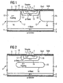
- FIGS. 1 to 3 show the invention with reference to an n-channel IGBTS. Of course, the invention can also be implemented on p-channel IGBTS.
- the semiconductor body of the semiconductor device is denoted by 1. It has an upper surface 3 and a lower surface 4. It has an n - doped inner zone 2, which adjoins the upper surface 3 of the semiconductor body 1.
- a p-doped base region 6 is embedded in the upper surface 3.
- two n + -doped emitter regions 7 are embedded.
- the base zones 6 and the emitter zones 7 are of Emitter electrodes 8 contacted, which consist of metal, such as aluminum.
- Adjacent to the lower surface 4 of the inner zone 2 is a p + -doped anode zone 5. This is connected via a metallization with a collector electrode 9. Left and right next to the base zone 6 are intermediate cell zones 12, the spatially separated periodically separate base zones spatially.
- a gate electrode 10 is disposed.
- the gate electrode 10 may be made of highly doped polysilicon or of metal.
- the base region 6 is embedded in a shielding zone 13, which is heavily doped n + .
- the shielding zone 13 has a significantly higher doping concentration than the surrounding inner zone 2.
- the shielding zone 13 has a left lateral edge 17 and a right lateral edge 18.
- the lower edge 16 of these floating regions 15 lies deep in the inner zone 2.
- the lower edge 16 of the floating regions 15 is arranged deeper in the inner zone than the lower edge 14 of the shielding zone 13.
- FIG. 2 shows an alternative embodiment of the present invention, wherein the floating region 15 is not arranged laterally adjacent to the shielding zone 13, but is located below the shielding zone 13 and above the anode zone 5.
- the floating region 15 is arranged here at a spatial distance to the lower edge of the shielding zone 14, whereas in the FIG. 3 an embodiment is shown in which the shielding zone 13 is embedded in the floating region 15.
- the doping concentration in the shielding zone 13 is substantially greater than in the inner zone 2.
- the doping concentration in the shielding zone 13 in all three embodiments shown has a value of about 10 17 / cm 3
- the doping concentration in the inner zone has a value of about 10 14 / cm 3 .
- a p-type dopant such as boron is implanted. Thereafter, the dopant is "driven” or diffused by a subsequent annealing step. In this driven p + -doped layer, which serves as a floating region 15, then a heavily doped n-type region 13 is driven. This strongly n-conducting region serves as the shielding zone 13. In turn, a weakly n-conducting layer is deposited epitaxially on this layer, which terminates the semiconductor body at the top.
- the base zone 5 is then embedded on the upper surface 3 of this layer and, in addition to the base zone 5, strongly n-conducting zones 13 ', 13 "are implanted via a further implantation at the lateral edges of the base zone. These heavily n-doped zones 13 ', 13''are in turn driven in such a way that they come into contact with the underlying strong n-zone. Finally, these areas then form the environment of the base zone. Subsequently, the semiconductor body thus produced is further processed at the top, ie the emitter regions, the emitter electrode, possibly short-circuit regions and the gate electrode are formed.
- this shielding zone 13 provides a structure which leads to a considerable increase in the minority carrier density on the cathode side of the IGBT, ie below the base zone 6.
- the resulting due to the concentration gradient between the shielding zone 13 and the inner zone 2 drift field causes the base zone 6 no longer acts as a sink for the minority carriers, which in the on state of the IGBT has a corresponding increase in the minority carrier result.
- unconnected floating regions 15 of the opposite conductivity type are introduced, either below the shielding zone 13 and above the anode zone 5 or adjacent to the base zones 6 in the intercell zones 12.
- non-connected floating regions 15 of the opposite conductivity type have a penetration depth which is significantly greater than the penetration depth of the shielding zone into the inner zone.
- the non-connected floating areas of opposite with respect to the shielding zone 13 conductivity type have the purpose that the areas directly on the cathode side, ie immediately below the base zone 6 are shielded, ie the course of the equipotential lines does not extend to the lower edge of the base zones 6. This achieves a high blocking resistance in addition to a very small V CESat .
Landscapes
- Bipolar Transistors (AREA)
- Thyristors (AREA)
- Electrodes Of Semiconductors (AREA)
Claims (5)
- Composant à semi-conducteur pouvant être commandé par effet de champ et constitué d'un corps (1) semi-conducteura) ayant une zone (2) intérieure du premier type de conductivité, qui est voisine de la surface (3) supérieure du corps (1) semi-conducteur,b) ayant une zone (5) d'anode du deuxième type de conductivité, qui est voisine de la surface (4) inférieure du corps (1) semi-conducteur,c) ayant au moins une zone (6) de base du deuxième type de conductivité, qui est incorporée dans la surface (3) supérieure du corps (1) semi-conducteur,d) ayant au moins une zone (7) d'émetteur du premier type de conductivité, qui est incorporée dans la zone (6) de base,e) ayant une électrode (8) d'émetteur, qui est disposée au-dessus de la surface (3) supérieure du corps (1) semi-conducteur et qui est reliée d'une manière conductrice à la zone (7) d'émetteur,f) ayant une électrode (9) de collecteur, qui est disposée sous la surface (4) inférieure du corps (1) semi-conducteur et qui est reliée de manière conductrice à la zone (5) d'anode, etg) ayant une électrode (10) de grille, qui est disposée au-dessus de la surface (3) supérieure du corps (1) semi-conducteur et qui recouvre à une distance isolante les parties de la zone (6) de base et de la zone (7) d'émetteur,
caractérisé en ce queh) la zone (6) de base est incorporée dans une zone (13) de protection du premier type de conductivité qui a une concentration de dopage plus grande que la zone (2) intérieure qui l'entoure, eti) il est prévu, dans la région de la zone (2) intérieure, au moins un domaine (15) flottant non raccordé de plus grande conductivité du deuxième type de conductivité et dont le bord (16) inférieur va plus profondément dans la zone (2) intérieure que le bord (14) inférieur de la zone (13) de protection. - Composant à semi-conducteur pouvant être commandé par effet de champ suivant la revendication 1,
caractérisé en ce que, dans le corps (1) semi-conducteur, sont disposées, suivant une périodicité de translation, une pluralité de zones (6) de base, de zones (7) d'émetteur et de zones (13) de protection, qui sont séparées dans l'espace par des zones (12) de cellules intermédiaires. - Composant à semi-conducteur pouvant être commandé par effet de champ suivant la revendication 1 ou 2,
caractérisé en ce que le domaine (15) flottant est disposé en dessous de la zone (13) de protection et au-dessus de la zone (5) d'anode. - Composant à semi-conducteur pouvant être commandé par effet de champ suivant la revendication 1 ou 2,
caractérisé en ce que le domaine (15) flottant est incorporé d'une manière séparée dans l'espace à côté de la zone (13) de protection, dans la zone (3) supérieure du corps (1) semi-conducteur. - Composant à semi-conducteur pouvant être commandé par effet de champ suivant la revendication 3 ou 4,
caractérisé en ce que la concentration de dopage de la zone (13) de protection est plus grande d'environ trois puissances de dix que la concentration de dopage de la zone (2) intérieure.
Applications Claiming Priority (3)
| Application Number | Priority Date | Filing Date | Title |
|---|---|---|---|
| DE19707513 | 1997-02-25 | ||
| DE19707513A DE19707513A1 (de) | 1997-02-25 | 1997-02-25 | Durch Feldeffekt steuerbares Halbleiterbauelement |
| PCT/DE1998/000244 WO1998038681A1 (fr) | 1997-02-25 | 1998-01-27 | Composant a semiconducteur pouvant etre commande par effet de champ |
Publications (2)
| Publication Number | Publication Date |
|---|---|
| EP0913000A1 EP0913000A1 (fr) | 1999-05-06 |
| EP0913000B1 true EP0913000B1 (fr) | 2008-04-16 |
Family
ID=7821420
Family Applications (1)
| Application Number | Title | Priority Date | Filing Date |
|---|---|---|---|
| EP98906848A Expired - Lifetime EP0913000B1 (fr) | 1997-02-25 | 1998-01-27 | Composant a semiconducteur pouvant etre commande par effet de champ |
Country Status (6)
| Country | Link |
|---|---|
| US (1) | US6147381A (fr) |
| EP (1) | EP0913000B1 (fr) |
| JP (1) | JP4108762B2 (fr) |
| KR (1) | KR100397882B1 (fr) |
| DE (2) | DE19707513A1 (fr) |
| WO (1) | WO1998038681A1 (fr) |
Families Citing this family (17)
| Publication number | Priority date | Publication date | Assignee | Title |
|---|---|---|---|---|
| DE19830332C2 (de) | 1998-07-07 | 2003-04-17 | Infineon Technologies Ag | Vertikales Halbleiterbauelement mit reduziertem elektrischem Oberflächenfeld |
| DE59914759D1 (de) * | 1998-10-26 | 2008-06-26 | Infineon Technologies Ag | Bipolares hochvolt-leistungsbauelement |
| WO2000035021A1 (fr) | 1998-12-04 | 2000-06-15 | Infineon Technologies Ag | Commutateur statique de puissance |
| DE19945639A1 (de) * | 1999-09-23 | 2001-04-05 | Abb Semiconductors Ag | Bipolartransistor mit isolierter Gateelektrode (IGBT) |
| DE10009347C2 (de) * | 2000-02-28 | 2003-11-13 | Infineon Technologies Ag | Verfahren zur Herstellung eines Halbleiterbauelements |
| JP3657938B2 (ja) | 2002-03-27 | 2005-06-08 | 株式会社東芝 | 半導体装置 |
| KR100900562B1 (ko) * | 2003-03-24 | 2009-06-02 | 페어차일드코리아반도체 주식회사 | 향상된 uis 내성을 갖는 모스 게이트형 트랜지스터 |
| US7569900B2 (en) * | 2004-11-16 | 2009-08-04 | Kabushiki Kaisha Toshiba | Silicon carbide high breakdown voltage semiconductor device |
| WO2006125330A1 (fr) | 2005-05-24 | 2006-11-30 | Abb Schweiz Ag | Conception de cellule cathodique |
| WO2012113818A2 (fr) | 2011-02-23 | 2012-08-30 | Abb Technology Ag | Dispositif semiconducteur de puissance et procédé de fabrication d'un tel dispositif semiconducteur de puissance |
| KR101241020B1 (ko) * | 2011-11-02 | 2013-03-11 | 현대자동차주식회사 | 모스펫 소자 및 그 제조 방법 |
| CN102683403B (zh) * | 2012-04-24 | 2015-05-27 | 电子科技大学 | 一种沟槽栅电荷存储型igbt |
| CN102842612A (zh) * | 2012-09-11 | 2012-12-26 | 电子科技大学 | 具有埋岛结构的绝缘栅双极型晶体管 |
| EP2889914A1 (fr) * | 2013-12-30 | 2015-07-01 | ABB Technology AG | Dispositif semi-conducteur bipolaire |
| JP6256075B2 (ja) * | 2014-02-13 | 2018-01-10 | 住友電気工業株式会社 | 炭化珪素半導体装置 |
| CN107369703B (zh) * | 2016-05-13 | 2020-12-04 | 株洲中车时代电气股份有限公司 | 载流子增强注入型igbt结构 |
| FR3102820B1 (fr) | 2019-10-30 | 2021-10-01 | Airbus Helicopters | Système de transmission de couple à multiples chemins de passage entre un arbre menant et un arbre mené et véhicule |
Family Cites Families (8)
| Publication number | Priority date | Publication date | Assignee | Title |
|---|---|---|---|---|
| US4364073A (en) * | 1980-03-25 | 1982-12-14 | Rca Corporation | Power MOSFET with an anode region |
| JPS57180164A (en) * | 1981-04-30 | 1982-11-06 | Nec Corp | Semiconductor device |
| US4821095A (en) * | 1987-03-12 | 1989-04-11 | General Electric Company | Insulated gate semiconductor device with extra short grid and method of fabrication |
| JPH06268227A (ja) * | 1993-03-10 | 1994-09-22 | Hitachi Ltd | 絶縁ゲート型バイポーラトランジスタ |
| DE4309764C2 (de) * | 1993-03-25 | 1997-01-30 | Siemens Ag | Leistungs-MOSFET |
| JPH0778978A (ja) * | 1993-09-07 | 1995-03-20 | Toyota Central Res & Dev Lab Inc | 縦型mos電界効果トランジスタ |
| US5751024A (en) * | 1995-03-14 | 1998-05-12 | Mitsubishi Denki Kabushiki Kaisha | Insulated gate semiconductor device |
| DE69512021T2 (de) * | 1995-03-31 | 2000-05-04 | Consorzio Per La Ricerca Sulla Microelettronica Nel Mezzogiorno, Catania | DMOS-Anordnung-Struktur und Verfahren zur Herstellung |
-
1997
- 1997-02-25 DE DE19707513A patent/DE19707513A1/de not_active Withdrawn
-
1998
- 1998-01-27 WO PCT/DE1998/000244 patent/WO1998038681A1/fr not_active Ceased
- 1998-01-27 EP EP98906848A patent/EP0913000B1/fr not_active Expired - Lifetime
- 1998-01-27 JP JP53714898A patent/JP4108762B2/ja not_active Expired - Fee Related
- 1998-01-27 DE DE59814220T patent/DE59814220D1/de not_active Expired - Lifetime
- 1998-01-27 KR KR10-1998-0708493A patent/KR100397882B1/ko not_active Expired - Fee Related
- 1998-11-06 US US09/187,501 patent/US6147381A/en not_active Expired - Lifetime
Also Published As
| Publication number | Publication date |
|---|---|
| DE59814220D1 (de) | 2008-05-29 |
| WO1998038681A1 (fr) | 1998-09-03 |
| KR100397882B1 (ko) | 2004-05-17 |
| KR20000064987A (ko) | 2000-11-06 |
| DE19707513A1 (de) | 1998-09-24 |
| US6147381A (en) | 2000-11-14 |
| EP0913000A1 (fr) | 1999-05-06 |
| JP2000509916A (ja) | 2000-08-02 |
| JP4108762B2 (ja) | 2008-06-25 |
Similar Documents
| Publication | Publication Date | Title |
|---|---|---|
| EP1114466B1 (fr) | Element semi-conducteur haute tension | |
| DE102009038731B4 (de) | Halbleiterbauelement mit Ladungsträgerkompensationsstruktur und Verfahren zur Herstellung eines Halbleiterbauelements | |
| DE102010039258B4 (de) | Transistorbauelement mit reduziertem Kurzschlussstrom | |
| DE102010064588B3 (de) | Halbleitervorrichtung mit einer potenzialfreien Halbleiterzone | |
| EP1408554B1 (fr) | Composant semi-conducteur commandé par effet de champ | |
| DE69414311T2 (de) | Halbleiteranordnung mit einer Bipolarfeldeffektanordnung mit isoliertem Gate | |
| DE69938562T3 (de) | Leistungshalbleiterbauelemente mit verbesserten Hochfrequenzschaltung- und Durchbruch-Eigenschaften | |
| DE10214151B4 (de) | Halbleiterbauelement mit erhöhter Durchbruchspannung im Randbereich | |
| DE102016125879B3 (de) | Halbleitervorrichtung mit einer IGBT-Region und einer nicht schaltbaren Diodenregion | |
| EP0913000B1 (fr) | Composant a semiconducteur pouvant etre commande par effet de champ | |
| DE102014104061B4 (de) | Bipolartransistor mit isolierter gateelektrode mit emitterkurzschlussbereichen | |
| DE102008039845A1 (de) | Halbleiterbauelement mit einem Halbleiterkörper | |
| DE102006050338A1 (de) | Halbleiterbauelement mit verbessertem Speicherladung zu Dioden-Softness Trade-off | |
| DE10322594A1 (de) | MIS-Halbleiterbauteil und Verfahren zu seiner Herstellung | |
| EP0760528B1 (fr) | Dispositif semi-conducteur sur base de silicium avec bordure à blocage élevé | |
| DE102020116653A1 (de) | Siliziumcarbid-halbleiterbauelement | |
| DE212021000529U1 (de) | Leistungshalbleitervorrichtung mit isolierter Graben-Gate-Elektrode | |
| DE102005041838B3 (de) | Halbleiterbauelement mit platzsparendem Randabschluss und Verfahren zur Herstellung eines solchen Bauelements | |
| DE19630341A1 (de) | Halbleitereinrichtung | |
| DE19534154C2 (de) | Durch Feldeffekt steuerbares Leistungs-Halbleiterbauelement | |
| DE10213534B4 (de) | Halbleiteraufbau mit Schaltelement und Randelement | |
| EP0206350A2 (fr) | Thyristor à épaisseur de base réduite | |
| DE102005029263B4 (de) | Halbleiterbauelement mit verbesserter dynamischer Belastbarkeit | |
| WO2001015235A1 (fr) | Composant a semi-conducteur de puissance a structure verticale | |
| DE102006014580B4 (de) | Vertikales Hochvolt-Halbleiterbauelement und Verfahren zur Herstellung eines Randabschlusses für einen IGBT |
Legal Events
| Date | Code | Title | Description |
|---|---|---|---|
| PUAI | Public reference made under article 153(3) epc to a published international application that has entered the european phase |
Free format text: ORIGINAL CODE: 0009012 |
|
| 17P | Request for examination filed |
Effective date: 19980814 |
|
| AK | Designated contracting states |
Kind code of ref document: A1 Designated state(s): DE FR GB IE IT |
|
| RAP1 | Party data changed (applicant data changed or rights of an application transferred) |
Owner name: INFINEON TECHNOLOGIES AG |
|
| GRAP | Despatch of communication of intention to grant a patent |
Free format text: ORIGINAL CODE: EPIDOSNIGR1 |
|
| RIC1 | Information provided on ipc code assigned before grant |
Ipc: H01L 29/06 20060101ALI20071015BHEP Ipc: H01L 29/10 20060101ALI20071015BHEP Ipc: H01L 29/739 20060101AFI20071015BHEP |
|
| GRAS | Grant fee paid |
Free format text: ORIGINAL CODE: EPIDOSNIGR3 |
|
| GRAA | (expected) grant |
Free format text: ORIGINAL CODE: 0009210 |
|
| AK | Designated contracting states |
Kind code of ref document: B1 Designated state(s): DE FR GB IE IT |
|
| REG | Reference to a national code |
Ref country code: IE Ref legal event code: FG4D Free format text: LANGUAGE OF EP DOCUMENT: GERMAN |
|
| REF | Corresponds to: |
Ref document number: 59814220 Country of ref document: DE Date of ref document: 20080529 Kind code of ref document: P |
|
| REG | Reference to a national code |
Ref country code: IE Ref legal event code: FD4D |
|
| PG25 | Lapsed in a contracting state [announced via postgrant information from national office to epo] |
Ref country code: IE Free format text: LAPSE BECAUSE OF FAILURE TO SUBMIT A TRANSLATION OF THE DESCRIPTION OR TO PAY THE FEE WITHIN THE PRESCRIBED TIME-LIMIT Effective date: 20080416 |
|
| PLBE | No opposition filed within time limit |
Free format text: ORIGINAL CODE: 0009261 |
|
| STAA | Information on the status of an ep patent application or granted ep patent |
Free format text: STATUS: NO OPPOSITION FILED WITHIN TIME LIMIT |
|
| EN | Fr: translation not filed | ||
| 26N | No opposition filed |
Effective date: 20090119 |
|
| PG25 | Lapsed in a contracting state [announced via postgrant information from national office to epo] |
Ref country code: IT Free format text: LAPSE BECAUSE OF FAILURE TO SUBMIT A TRANSLATION OF THE DESCRIPTION OR TO PAY THE FEE WITHIN THE PRESCRIBED TIME-LIMIT Effective date: 20080416 |
|
| GBPC | Gb: european patent ceased through non-payment of renewal fee |
Effective date: 20090127 |
|
| PG25 | Lapsed in a contracting state [announced via postgrant information from national office to epo] |
Ref country code: GB Free format text: LAPSE BECAUSE OF NON-PAYMENT OF DUE FEES Effective date: 20090127 |
|
| PG25 | Lapsed in a contracting state [announced via postgrant information from national office to epo] |
Ref country code: FR Free format text: LAPSE BECAUSE OF FAILURE TO SUBMIT A TRANSLATION OF THE DESCRIPTION OR TO PAY THE FEE WITHIN THE PRESCRIBED TIME-LIMIT Effective date: 20090227 |
|
| PGFP | Annual fee paid to national office [announced via postgrant information from national office to epo] |
Ref country code: DE Payment date: 20140318 Year of fee payment: 17 |
|
| REG | Reference to a national code |
Ref country code: DE Ref legal event code: R119 Ref document number: 59814220 Country of ref document: DE |
|
| PG25 | Lapsed in a contracting state [announced via postgrant information from national office to epo] |
Ref country code: DE Free format text: LAPSE BECAUSE OF NON-PAYMENT OF DUE FEES Effective date: 20150801 |