EP0360477B1 - Energieversorgungskontakt für integrierte Schaltungen - Google Patents
Energieversorgungskontakt für integrierte Schaltungen Download PDFInfo
- Publication number
- EP0360477B1 EP0360477B1 EP89309221A EP89309221A EP0360477B1 EP 0360477 B1 EP0360477 B1 EP 0360477B1 EP 89309221 A EP89309221 A EP 89309221A EP 89309221 A EP89309221 A EP 89309221A EP 0360477 B1 EP0360477 B1 EP 0360477B1
- Authority
- EP
- European Patent Office
- Prior art keywords
- substrate
- integrated circuit
- power supply
- epitaxial layer
- tub
- Prior art date
- Legal status (The legal status is an assumption and is not a legal conclusion. Google has not performed a legal analysis and makes no representation as to the accuracy of the status listed.)
- Expired - Lifetime
Links
Images

Classifications
-
- H—ELECTRICITY
- H10—SEMICONDUCTOR DEVICES; ELECTRIC SOLID-STATE DEVICES NOT OTHERWISE PROVIDED FOR
- H10W—GENERIC PACKAGES, INTERCONNECTIONS, CONNECTORS OR OTHER CONSTRUCTIONAL DETAILS OF DEVICES COVERED BY CLASS H10
- H10W20/00—Interconnections in chips, wafers or substrates
- H10W20/40—Interconnections external to wafers or substrates, e.g. back-end-of-line [BEOL] metallisations or vias connecting to gate electrodes
- H10W20/482—Interconnections external to wafers or substrates, e.g. back-end-of-line [BEOL] metallisations or vias connecting to gate electrodes for individual devices provided for in groups H10D8/00 - H10D48/00, e.g. for power transistors
- H10W20/484—Interconnections having extended contours, e.g. pads having mesh shape or interconnections comprising connected parallel stripes
-
- H—ELECTRICITY
- H10—SEMICONDUCTOR DEVICES; ELECTRIC SOLID-STATE DEVICES NOT OTHERWISE PROVIDED FOR
- H10W—GENERIC PACKAGES, INTERCONNECTIONS, CONNECTORS OR OTHER CONSTRUCTIONAL DETAILS OF DEVICES COVERED BY CLASS H10
- H10W20/00—Interconnections in chips, wafers or substrates
- H10W20/40—Interconnections external to wafers or substrates, e.g. back-end-of-line [BEOL] metallisations or vias connecting to gate electrodes
- H10W20/41—Interconnections external to wafers or substrates, e.g. back-end-of-line [BEOL] metallisations or vias connecting to gate electrodes characterised by their conductive parts
- H10W20/427—Power or ground buses
Definitions
- the present invention relates to an improved method of providing an electrical power contact to an integrated circuit.
- a power conductor is routed around the "front" side of the chip; i.e, the side on which the field effect devices are formed.
- the power conductor connects the devices to a bondpad from which a wire lead connects to an integrated circuit package terminal, for connection to an external power supply.
- At least one power conductor, or "bus" is provided for each power supply voltage.
- usually several bonding pads are provided to connect a given bus with the package power supply terminals. For example, in one current microprocessor design, 15 V SS bondpads must be provided out of a total of 130 bondpads.
- the integrated circuit chips have now become “bondpad limited", with the periphery of the chip supporting the maximum number of bondpads possible. Hence, the large number of power supply bondpads reduce the number available for other purposes, such as signal inputs and outputs.
- an additional concern relates to electrical noise generated when output buffers turn on or off.
- Such switching noise voltages are due in part to the rapid change in current flow through the power supply conductors, which causes switching noise voltages to occur due to ohmic voltage drop across the resistance of the conductor, and to the inductive voltage produced by the inductance of the conductor.
- Such noise voltages can interfere with the other signals internal to the integrated circuit, or with the output signals from other output buffers.
- the change in current through the ground (V SS ) power supply conductor causes "ground bounce" noise to be generated, wherein the internal ground potential bounces with respect to the external ground.
- ground bounce noise is known to be caused in significant part by the switching of the output buffers, since they momentarily draw a relatively large current in order to charge up the capacitance of the external output lead to which they are connected.
- a bus has been split into two or more portions connected to different areas of the integrated circuit, in an attempt to isolate the noise generated in one area from affecting devices in another area.
- bipolar devices may be supplied with a positive power supply voltage (V CC ) by a metallic contact on the back side of an integrated circuit chip. This allows contacting a buried collector region that is formed in an epitaxial layer on the substrate.
- V CC positive power supply voltage
- the high resistivity of the epitaxial layer prevents the power supply voltage V CC from being supplied to devices located on the top surface (front) of the chip. For example, a resistor requires a separate surface contact thereto.
- CMOS integrated circuits are frequently formed on semiconductor substrates that have an epitaxial layer.
- the p and n channel devices are formed in doped "tub" regions located in the epitaxial layer.
- the epitaxial layer formed by deposition onto a single crystal semiconductor wafer, is usually much less heavily doped than the wafer, with the tubs having a doping level intermediate between that of the wafer and the epitaxial layer.
- the epitaxial layer has a much higher resistivity than the wafer.
- the number of V SS and V DD power supply bonding wires is chosen based upon a calculation of the maximum inductance that can be tolerated for acceptable ground-bounce performance.
- a conductive (e.g., metal) layer on the back side of an integrated circuit substrate is connected to a power supply terminal.
- power supply current is provided to the source electrodes of field effect devices through the substrate.
- the epitaxial layer typically has a resistivity at least 100 times greater than the substrate.
- fewer power supply bondpads are required than called for by prior art design techniques. The bondpads may even be eliminated for a given power supply voltage in some cases.
- FIG. 1 shows a cross section of a CMOS integrated circuit having a source region contacted by the inventive technique.
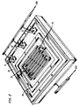
- FIG. 2 shows power busses and external power supply connections to an integrated circuit chip that employs the inventive technique.
- CMOS integrated circuits having a power supply voltage conducted to field effect devices formed in a tub located in a relatively lightly doped epitaxial layer formed on a more heavily doped substrate.
- conduction through the lightly doped (i.e., higher resistivity) substrate can be sufficient to provide the channel current for device operation. This is the case even when the doping level of the epitaxial layer is over two orders of magnitude less than the substrate, so that the resistivity of the epitaxial layer is over 100 times greater than the substrate.
- successful operation may be obtained using an epitaxial layer having a resistivity over 1000 times greater than the substrate (e.g., having a doping level over 1000 times less).
- latch-up suppression of a CMOS integrated circuit is not impaired by the present technique, even though large currents flow vertically through the substrate.
- power supply bounce, and hence noise is typically reduced, due to reduced lead inductance.
- a silicon substrate 101 has a metallic layer 100 covering the "back" side of the substrate, which is connected through a package terminal to the negative power supply V SS .
- An epitaxial layer 113 is formed on the "front" side of the substrate; the doping level of the epitaxial layer is significantly less than that of the substrate, resulting in a much higher resistivity.
- Field effect devices are formed in "tubs", being doped regions located in the epitaxial layer. In particular, the p-channel field effect transistors are formed in the n-tub 102, and the n-channel field effect transistors are formed in the p-tub 103.
- the source region 104 of the n-channel devices is connected to a highly doped tub contact region 105 by means of a conductor 112, forming a "tub-tie".
- a tub-tie per se is known in the art, for causing the tub to be held at a desired potential, in order to provide a constant back-gate bias.
- the highly doped contact region is often made minimum size, in order to save space.
- the highly doped tub contact region 105 is desirably made large compared to prior art practice. I recommend that the width and length of region 105 be made approximately equal to that of the overlying power bus (when present).
- the channel current to the inverter (I inv ) is then conducted through the contact window 106 to the p-tub with minimal voltage drop.
- the conductor 112 may be of suitable material for providing a low resistance ohmic contact between the source 104 and the highly doped contact region 105.
- the conductor is a metal (e.g., aluminum) that extends through contact windows in an overlying dielectric in order to contact these regions, and may form part of the power (e.g., V SS ) bus.
- V SS power bus
- the silicide may be formed during the "salicide" process that forms the silicide layer on the gate, source, and drain. In that case, the silicide is located underneath the dielectric layer, and the contact windows may be omitted entirely, unless additional conduction by means of the conventional power supply bus is also desired.
- the other regions of FIG. 1 included in the exemplary inverter are the gate electrodes 117 and 118 for the n-channel and p-channel devices, respectively.
- the source 116 of the p-channel device is connected to the V DD bus 108, which is connected by means of a conventional tub tie window 114 to the n+ tub contact region 109.
- the dopant type typically remains the same from the tub contact region (and hence the tub) into the epitaxial layer and substrate. That is, the doping is continuously p-type in the exemplary case, with no reverse-biased p-n junctions being present that would interfere with power supply current conduction. Hence, the current may flow from the source of the n-channel transistors in the p-tub to the p-tub contact region (by means of the ohmic contact provided by the tub tie conductor), and through both the epitaxial layer and substrate to the V SS contact on the back side of the chip.
- n-type substrate were used having an n-type epitaxial layer thereon, then a suitably sized n-tub contact region could be used to provide conduction to the positive (V DD ) power supply voltage for the p-channel devices.
- V DD positive
- the resistance of a cross-sectional slab of silicon in the p-tub has been estimated for two CMOS technologies, having nominal linewidths of 0.9 micrometers and 1.25 micrometers, respectively (also referred to as the "0.9 micron technology” and the “1.25 micron technology” herein).
- the slab had a length of 100 micrometers and a width of 100 micrometers as viewed from the front (top) side of the silicon chip, and extended from the front side to the back side contact.
- the p+ tub contact region was assumed to cover the entire top surface.
- the doping level of the p+ substrate was on the order of 1X10 19 per cm 3 , whereas in the p epitaxial layer it was on the order of 1X10 15 per cm 3 .
- the thickness of the epitaxial layer was 7 micrometers for the 0.9 micron technology prior to the tub diffusion. After the tub diffusion, the thickness of the lightly doped epitaxial layer under the tub was about 1 micrometer.
- the doping level of the p+ substrate was 1X10 19 per cm 3 , whereas in the p epitaxial layer it was 5X10 14 per cm 3 .
- the thickness of the epitaxial layer was 16 micrometers for the 1.25 micron technology, and after tub diffusion the thickness under the tub was 10 micrometers. Note that for both technologies, the doping level of the epitaxial layer was over 1000 times less than that of the substrate, so that the resistivity of the epitaxial layer was more than 1000 times greater than that of the substrate.
- the results are listed in the Table below: TABLE RESISTANCE OF LAYERS Technology p+ contact p-tub p-epi p+ substrate Total 0.9 micron 0.0007 2.0 24 5 31 ohms 1.25 micron 0.0027 3.5 250 4.1 262 ohms
- the worst case resistance between the metal V SS bus and the p+ tub contact region is 10 ohms per contact.
- the tub tie contacts are placed once every 20 micrometers, the total contact resistance is 0.4 ohms, which is negligible.
- the present technique thus allows for a reduction in the number of bondpads devoted to power supply conductors.
- V DD e.g., 31-33
- the bondpads connected to V DD may be needed on the front side (top side as viewed) of the chip.
- V DD typically connected to the "I/O frame V DD bus" 34, which in turn is typically connected to the interior portions of the circuitry through an "interior bus” 35, with various other configurations being possible.
- the present technique need not result in a complete elimination of bondpads for the given power supply voltage.
- the V SS bus may be split into two (or more) portions, with one or more bondpads connected to the portions that require extra current capacity.
- the I/O frame bus may still be connected to bondpads, with the interior bus portions then not being connected (as by conductor 38) to the I/O frame bus, but rather relying on the substrate conduction according to the present invention.
- the present technique may still allow a reduction in the number of bondpads required, as compared to the prior art practice of relying solely on current conduction through the bondpads. I estimate that in a typical case, the number of bondpads required for the given power supply voltage that uses the substrate conduction will be less than half the number required by prior art design techniques.
- a CMOS integrated circuit is formed using the twin-tub process.
- Other techniques including single tub (or single "well”) techniques are known, and may also be utilized with the present invention.
- the n-tub is present, with the p-channel devices being formed therein, and the n-channel devices being formed in the surrounding portion of the p-type epitaxial layer.
- the V SS power supply connection may still be provided through the p+ substrate, by providing a highly doped (p+) contact region in the epitaxial layer and connecting it to the sources of the n channel devices.
- the epitaxial layer for the single tub case is typically doped more highly than for the twin-tub case, although still much less than the substrate.
- the doping level of the epitaxial layer is in the range of 1X10 14 per cm 3 to 1X10 17 per cm 3 , while that of the substrate is typically at least 5X10 18 per cm 3 .
- the epitaxial layer typically has a doping level of less than 1x10 16 per cm 3 ).
- the conductive layer on the back side of the integrated circuit is typically a metal, other materials (e.g., silicides) are possible.
- the present technique also offers advantages in terms of electromigration resistance of the power supply conductors. That is, the conductors may be made smaller than in prior art practice, since a portion of the current may be conducted through the substrate according to the inventive technique.
Landscapes
- Metal-Oxide And Bipolar Metal-Oxide Semiconductor Integrated Circuits (AREA)
- Semiconductor Integrated Circuits (AREA)
- Internal Circuitry In Semiconductor Integrated Circuit Devices (AREA)
- Bipolar Transistors (AREA)
Claims (10)
- Integrierte Schaltung mit:einem Halbleitersubstrat (101) mit einem gegebenen Leitfähigkeitstyp und relativ niedrigem spezifischen Widerstand;einer Epitaxialschicht (113), die auf der Vorderseite des besagten Substrats ausgebildet ist und einen spezifischen Widerstand aufweist, der mindestens 100 mal größer ist als der spezifische Widerstand des Substrats;mindestens einem Wannenbereich (103) mit dem besagten gegebenen Leitfähigkeitstyp, der in der besagten Epitaxialschicht ausgebildet ist und sich bis auf einen Abstand (d) zu dem besagten Substrat erstreckt, wobei der Abstand (d) weniger als 15 Mikrometer beträgt;mindestens einem stark dotierten Kontaktbereich (106) mit dem besagten gegebenen Leitfähigkeitstyp, der in dem besagten Wannenbereich ausgebildet ist;und Feldeffekttransistoren mit Source-Bereichen (104) des entgegenge-setzten Leitfähigkeitstyps, die in dem besagten Wannenbereich ausgebildet sind und mit dem besagten stark dotierten Kontaktbereich verbunden sind;und weiterhin mit einer leitenden Schicht (100), die auf der Hinterseite des besagten Substrats ausgebildet ist, mit Mitteln zum Verbinden der besagten leitenden Schicht mit einer Versorgungsspannung (VSS),wobei die besagte integrierte Schaltung auf der Vorderseite des besagten Substrats eine gegebene Anzahl von Versorgungsspannungsbondkontaktstellen (31...33) zur Verbindung mit externen Gehäuseanschlüssen aufweist, wobei die Funktion der besagten integrierten Schaltung eine Anzahl von Versorgungsspannungsbondkontaktstellen erfordert, die größer ist als die besagte gegebene Anzahl, jedoch für den Stromfluß durch die besagte leitende Schicht und das besagte Substrat hindurch zu den besagten Source-Bereichen.
- Integrierte Schaltung nach Anspruch 1, wobei mindestens manchen der besagten Transistoren allein durch den besagten Stromfluß durch die besagte leitende Schicht und das besagte Substrat im Betrieb Sourcestrom zugeführt wird.
- Integrierte Schaltung nach Anspruch 1, wobei der Abstand (d) von dem Boden des besagten Wannenbereichs zu der Schnittstelle zwischen der besagten Epitaxialschicht und dem besagten Substrat weniger als 5 Mikrometer beträgt.
- Integrierte Schaltung nach Anspruch 1, wobei der spezifische Widerstand der besagten Epitaxialschicht größer als 1000 mal der spezifische Widerstand des Grundmaterials des besagten Substrats ist.
- Integrierte Schaltung nach Anspruch 1, wobei die Dicke der besagten Epitaxialschicht nicht mehr als 10 Mikrometer beträgt.
- Integrierte Schaltung nach Anspruch 1, wobei die Dicke der besagten Epitaxialschicht weniger als 5 Mikrometer beträgt.
- Integrierte Schaltung nach Anspruch 1, wobei der besagte Leitfähigkeitstyp der p-Typ ist und die besagte Versorgungsspannung eine negative Spannung ist (VSS).
- Integrierte Schaltung nach Anspruch 7, die auf der Vorderseite des besagten Substrats keine Bondkontaktstellen für negative Versorgungsspannungen aufweist.
- Integrierte Schaltung nach Anspruch 1, wobei der besagte Leitfähigkeitstyp der n-Typ ist und die besagte Versorgungsspannung eine positive Spannung ist (VDD).
- Integrierte Schaltung nach Anspruch 9, die auf der Vorderseite des besagten Substrats keine Bondkontaktstellen für positive Versorgungsspannungen aufweist.
Applications Claiming Priority (2)
| Application Number | Priority Date | Filing Date | Title |
|---|---|---|---|
| US246713 | 1988-09-20 | ||
| US07/246,713 US4947228A (en) | 1988-09-20 | 1988-09-20 | Integrated circuit power supply contact |
Publications (3)
| Publication Number | Publication Date |
|---|---|
| EP0360477A2 EP0360477A2 (de) | 1990-03-28 |
| EP0360477A3 EP0360477A3 (de) | 1991-11-21 |
| EP0360477B1 true EP0360477B1 (de) | 1997-12-10 |
Family
ID=22931887
Family Applications (1)
| Application Number | Title | Priority Date | Filing Date |
|---|---|---|---|
| EP89309221A Expired - Lifetime EP0360477B1 (de) | 1988-09-20 | 1989-09-12 | Energieversorgungskontakt für integrierte Schaltungen |
Country Status (6)
| Country | Link |
|---|---|
| US (1) | US4947228A (de) |
| EP (1) | EP0360477B1 (de) |
| JP (1) | JP2738416B2 (de) |
| DE (1) | DE68928483T2 (de) |
| ES (1) | ES2110948T3 (de) |
| HK (1) | HK1002542A1 (de) |
Families Citing this family (17)
| Publication number | Priority date | Publication date | Assignee | Title |
|---|---|---|---|---|
| US5181094A (en) * | 1988-09-29 | 1993-01-19 | Mitsubishi Denki Kabushiki Kaisha | Complementary semiconductor device having improved device isolating region |
| US5574633A (en) * | 1994-02-23 | 1996-11-12 | At&T Global Information Solubions Company | Multi-phase charge sharing method and apparatus |
| US5985724A (en) * | 1996-10-01 | 1999-11-16 | Advanced Micro Devices, Inc. | Method for forming asymmetrical p-channel transistor having nitrided oxide patterned to selectively form a sidewall spacer |
| US5877930A (en) * | 1997-03-27 | 1999-03-02 | Digital Equipment Corporation | Input and output noise reduction circuit |
| US5970347A (en) * | 1997-07-18 | 1999-10-19 | Advanced Micro Devices, Inc. | High performance mosfet transistor fabrication technique |
| US6794978B2 (en) * | 2002-05-15 | 2004-09-21 | John C. Tung | Accurate multi-ground inductors for high-speed integrated circuits |
| US7400047B2 (en) * | 2004-12-13 | 2008-07-15 | Agere Systems Inc. | Integrated circuit with stacked-die configuration utilizing substrate conduction |
| US8008070B2 (en) * | 2007-12-07 | 2011-08-30 | METAMEMS Corp. | Using coulomb forces to study charateristics of fluids and biological samples |
| US8531848B2 (en) * | 2007-12-07 | 2013-09-10 | METAMEMS Corp. | Coulomb island and Faraday shield used to create adjustable Coulomb forces |
| US20090149038A1 (en) * | 2007-12-07 | 2009-06-11 | Metamems Llc | Forming edge metallic contacts and using coulomb forces to improve ohmic contact |
| US8159809B2 (en) * | 2007-12-07 | 2012-04-17 | METAMEMS Corp. | Reconfigurable system that exchanges substrates using coulomb forces to optimize a parameter |
| US7946174B2 (en) * | 2007-12-07 | 2011-05-24 | METAMEMS Corp. | Decelerometer formed by levitating a substrate into equilibrium |
| US7863651B2 (en) | 2007-12-07 | 2011-01-04 | METAMEMS Corp. | Using multiple coulomb islands to reduce voltage stress |
| US7965489B2 (en) * | 2007-12-07 | 2011-06-21 | METAMEMS Corp. | Using coulomb forces to form 3-D reconfigurable antenna structures |
| US8018009B2 (en) * | 2007-12-07 | 2011-09-13 | METAMEMS Corp. | Forming large planar structures from substrates using edge Coulomb forces |
| US7728427B2 (en) * | 2007-12-07 | 2010-06-01 | Lctank Llc | Assembling stacked substrates that can form cylindrical inductors and adjustable transformers |
| US7812336B2 (en) * | 2007-12-07 | 2010-10-12 | METAMEMS Corp. | Levitating substrate being charged by a non-volatile device and powered by a charged capacitor or bonding wire |
Family Cites Families (7)
| Publication number | Priority date | Publication date | Assignee | Title |
|---|---|---|---|---|
| JPS57162360A (en) * | 1981-03-31 | 1982-10-06 | Nec Corp | Complementary insulated gate field effect semiconductor device |
| JPS58157151A (ja) * | 1982-03-15 | 1983-09-19 | Mitsubishi Electric Corp | 半導体集積回路装置 |
| WO1984001053A1 (fr) * | 1982-08-26 | 1984-03-15 | Mitsubishi Electric Corp | Dispositif a semiconducteurs |
| US4572972A (en) * | 1983-01-18 | 1986-02-25 | At&T Laboratories | CMOS Logic circuits with all pull-up transistors integrated in separate chip from all pull-down transistors |
| JPS60152055A (ja) * | 1984-01-20 | 1985-08-10 | Matsushita Electric Ind Co Ltd | 相補型mos半導体装置 |
| US4631570A (en) * | 1984-07-03 | 1986-12-23 | Motorola, Inc. | Integrated circuit having buried oxide isolation and low resistivity substrate for power supply interconnection |
| US4675717A (en) * | 1984-10-09 | 1987-06-23 | American Telephone And Telegraph Company, At&T Bell Laboratories | Water-scale-integrated assembly |
-
1988
- 1988-09-20 US US07/246,713 patent/US4947228A/en not_active Expired - Lifetime
-
1989
- 1989-09-12 ES ES89309221T patent/ES2110948T3/es not_active Expired - Lifetime
- 1989-09-12 EP EP89309221A patent/EP0360477B1/de not_active Expired - Lifetime
- 1989-09-12 DE DE68928483T patent/DE68928483T2/de not_active Expired - Fee Related
- 1989-09-20 JP JP1242389A patent/JP2738416B2/ja not_active Expired - Lifetime
-
1998
- 1998-02-26 HK HK98101488A patent/HK1002542A1/en not_active IP Right Cessation
Also Published As
| Publication number | Publication date |
|---|---|
| JP2738416B2 (ja) | 1998-04-08 |
| EP0360477A2 (de) | 1990-03-28 |
| US4947228A (en) | 1990-08-07 |
| DE68928483T2 (de) | 1998-04-02 |
| JPH02114661A (ja) | 1990-04-26 |
| HK1002542A1 (en) | 1998-08-28 |
| ES2110948T3 (es) | 1998-03-01 |
| EP0360477A3 (de) | 1991-11-21 |
| DE68928483D1 (de) | 1998-01-22 |
Similar Documents
| Publication | Publication Date | Title |
|---|---|---|
| EP0360477B1 (de) | Energieversorgungskontakt für integrierte Schaltungen | |
| US5060037A (en) | Output buffer with enhanced electrostatic discharge protection | |
| US4990802A (en) | ESD protection for output buffers | |
| US6653670B2 (en) | Silicon-on-insulator diodes and ESD protection circuits | |
| US4672584A (en) | CMOS integrated circuit | |
| HK1002542B (en) | Integrated circuit power supply contact | |
| US5701024A (en) | Electrostatic discharge (ESD) protection structure for high voltage pins | |
| US6365940B1 (en) | High voltage trigger remote-cathode SCR | |
| US4806999A (en) | Area efficient input protection | |
| EP0242383B1 (de) | Schutz eines igfet integrierten schaltkreises vor elektrostatischer entladung | |
| US6611027B2 (en) | Protection transistor with improved edge structure | |
| US20060028776A1 (en) | Electrostatic discharge protection for an integrated circuit | |
| US4733285A (en) | Semiconductor device with input and/or output protective circuit | |
| EP0371663B1 (de) | Ausgangspuffer einer integrierten Schaltung mit einem verbesserten ESD-Schutz | |
| US5227327A (en) | Method for making high impedance pull-up and pull-down input protection resistors for active integrated circuits | |
| US5828108A (en) | Semiconductor integrated circuit suppressing noises due to short-circuit/substrate currents | |
| US5083179A (en) | CMOS semiconductor integrated circuit device | |
| US6084270A (en) | Semiconductor integrated-circuit device having n-type and p-type semiconductor conductive regions formed in contact with each other | |
| EP0606667A1 (de) | Halbleiterbauelement mit einer integrierten Schaltung mit Überspannungsschutz | |
| GB2243485A (en) | Semiconductor device contact pads | |
| CA1289267C (en) | Latchup and electrostatic discharge protection structure | |
| US5121179A (en) | Higher impedance pull-up and pull-down input protection resistors for MIS transistor integrated circuits | |
| US7180137B2 (en) | Semiconductor device | |
| US5500548A (en) | Non-epitaxial CMOS structures and processors | |
| KR0164591B1 (ko) | 집적회로 |
Legal Events
| Date | Code | Title | Description |
|---|---|---|---|
| PUAI | Public reference made under article 153(3) epc to a published international application that has entered the european phase |
Free format text: ORIGINAL CODE: 0009012 |
|
| AK | Designated contracting states |
Kind code of ref document: A2 Designated state(s): DE ES FR GB IT NL |
|
| PUAL | Search report despatched |
Free format text: ORIGINAL CODE: 0009013 |
|
| AK | Designated contracting states |
Kind code of ref document: A3 Designated state(s): DE ES FR GB IT NL |
|
| RHK1 | Main classification (correction) |
Ipc: H01L 23/48 |
|
| 17P | Request for examination filed |
Effective date: 19920511 |
|
| RAP3 | Party data changed (applicant data changed or rights of an application transferred) |
Owner name: AT&T CORP. |
|
| 17Q | First examination report despatched |
Effective date: 19940819 |
|
| GRAG | Despatch of communication of intention to grant |
Free format text: ORIGINAL CODE: EPIDOS AGRA |
|
| GRAG | Despatch of communication of intention to grant |
Free format text: ORIGINAL CODE: EPIDOS AGRA |
|
| GRAH | Despatch of communication of intention to grant a patent |
Free format text: ORIGINAL CODE: EPIDOS IGRA |
|
| GRAH | Despatch of communication of intention to grant a patent |
Free format text: ORIGINAL CODE: EPIDOS IGRA |
|
| GRAA | (expected) grant |
Free format text: ORIGINAL CODE: 0009210 |
|
| AK | Designated contracting states |
Kind code of ref document: B1 Designated state(s): DE ES FR GB IT NL |
|
| ITF | It: translation for a ep patent filed | ||
| ET | Fr: translation filed | ||
| REF | Corresponds to: |
Ref document number: 68928483 Country of ref document: DE Date of ref document: 19980122 |
|
| REG | Reference to a national code |
Ref country code: ES Ref legal event code: FG2A Ref document number: 2110948 Country of ref document: ES Kind code of ref document: T3 |
|
| PLBE | No opposition filed within time limit |
Free format text: ORIGINAL CODE: 0009261 |
|
| STAA | Information on the status of an ep patent application or granted ep patent |
Free format text: STATUS: NO OPPOSITION FILED WITHIN TIME LIMIT |
|
| 26N | No opposition filed | ||
| PGFP | Annual fee paid to national office [announced via postgrant information from national office to epo] |
Ref country code: NL Payment date: 20010828 Year of fee payment: 13 |
|
| PGFP | Annual fee paid to national office [announced via postgrant information from national office to epo] |
Ref country code: ES Payment date: 20010904 Year of fee payment: 13 |
|
| REG | Reference to a national code |
Ref country code: GB Ref legal event code: IF02 |
|
| PG25 | Lapsed in a contracting state [announced via postgrant information from national office to epo] |
Ref country code: ES Free format text: LAPSE BECAUSE OF NON-PAYMENT OF DUE FEES Effective date: 20020913 |
|
| PG25 | Lapsed in a contracting state [announced via postgrant information from national office to epo] |
Ref country code: NL Free format text: LAPSE BECAUSE OF NON-PAYMENT OF DUE FEES Effective date: 20030401 |
|
| REG | Reference to a national code |
Ref country code: ES Ref legal event code: FD2A Effective date: 20031011 |
|
| PGFP | Annual fee paid to national office [announced via postgrant information from national office to epo] |
Ref country code: DE Payment date: 20070921 Year of fee payment: 19 |
|
| PGFP | Annual fee paid to national office [announced via postgrant information from national office to epo] |
Ref country code: GB Payment date: 20070914 Year of fee payment: 19 |
|
| PGFP | Annual fee paid to national office [announced via postgrant information from national office to epo] |
Ref country code: IT Payment date: 20070924 Year of fee payment: 19 |
|
| PGFP | Annual fee paid to national office [announced via postgrant information from national office to epo] |
Ref country code: FR Payment date: 20070914 Year of fee payment: 19 |
|
| GBPC | Gb: european patent ceased through non-payment of renewal fee |
Effective date: 20080912 |
|
| REG | Reference to a national code |
Ref country code: FR Ref legal event code: ST Effective date: 20090529 |
|
| PG25 | Lapsed in a contracting state [announced via postgrant information from national office to epo] |
Ref country code: IT Free format text: LAPSE BECAUSE OF NON-PAYMENT OF DUE FEES Effective date: 20080912 Ref country code: DE Free format text: LAPSE BECAUSE OF NON-PAYMENT OF DUE FEES Effective date: 20090401 |
|
| PG25 | Lapsed in a contracting state [announced via postgrant information from national office to epo] |
Ref country code: FR Free format text: LAPSE BECAUSE OF NON-PAYMENT OF DUE FEES Effective date: 20080930 |
|
| PG25 | Lapsed in a contracting state [announced via postgrant information from national office to epo] |
Ref country code: GB Free format text: LAPSE BECAUSE OF NON-PAYMENT OF DUE FEES Effective date: 20080912 |