EP0361461B1 - Verfahren zur Herstellung von Metall-Polyimid-Verbundwerkstoffen - Google Patents
Verfahren zur Herstellung von Metall-Polyimid-Verbundwerkstoffen Download PDFInfo
- Publication number
- EP0361461B1 EP0361461B1 EP89117907A EP89117907A EP0361461B1 EP 0361461 B1 EP0361461 B1 EP 0361461B1 EP 89117907 A EP89117907 A EP 89117907A EP 89117907 A EP89117907 A EP 89117907A EP 0361461 B1 EP0361461 B1 EP 0361461B1
- Authority
- EP
- European Patent Office
- Prior art keywords
- residue
- polyimide
- film
- copper
- precursor
- Prior art date
- Legal status (The legal status is an assumption and is not a legal conclusion. Google has not performed a legal analysis and makes no representation as to the accuracy of the status listed.)
- Expired - Lifetime
Links
Images
Classifications
-
- H—ELECTRICITY
- H05—ELECTRIC TECHNIQUES NOT OTHERWISE PROVIDED FOR
- H05K—PRINTED CIRCUITS; CASINGS OR CONSTRUCTIONAL DETAILS OF ELECTRIC APPARATUS; MANUFACTURE OF ASSEMBLAGES OF ELECTRICAL COMPONENTS
- H05K1/00—Printed circuits
- H05K1/02—Details
- H05K1/03—Use of materials for the substrate
- H05K1/0313—Organic insulating material
- H05K1/032—Organic insulating material consisting of one material
- H05K1/0346—Organic insulating material consisting of one material containing N
-
- H—ELECTRICITY
- H01—ELECTRIC ELEMENTS
- H01B—CABLES; CONDUCTORS; INSULATORS; SELECTION OF MATERIALS FOR THEIR CONDUCTIVE, INSULATING OR DIELECTRIC PROPERTIES
- H01B1/00—Conductors or conductive bodies characterised by the conductive materials; Selection of materials as conductors
- H01B1/20—Conductive material dispersed in non-conductive organic material
- H01B1/22—Conductive material dispersed in non-conductive organic material the conductive material comprising metals or alloys
-
- H—ELECTRICITY
- H01—ELECTRIC ELEMENTS
- H01B—CABLES; CONDUCTORS; INSULATORS; SELECTION OF MATERIALS FOR THEIR CONDUCTIVE, INSULATING OR DIELECTRIC PROPERTIES
- H01B3/00—Insulators or insulating bodies characterised by the insulating materials; Selection of materials for their insulating or dielectric properties
- H01B3/18—Insulators or insulating bodies characterised by the insulating materials; Selection of materials for their insulating or dielectric properties mainly consisting of organic substances
- H01B3/30—Insulators or insulating bodies characterised by the insulating materials; Selection of materials for their insulating or dielectric properties mainly consisting of organic substances plastics; resins; waxes
- H01B3/303—Macromolecular compounds obtained by reactions forming a linkage containing nitrogen with or without oxygen or carbon in the main chain of the macromolecule, not provided for in groups H01B3/38 or H01B3/302
- H01B3/306—Polyimides or polyesterimides
-
- H—ELECTRICITY
- H10—SEMICONDUCTOR DEVICES; ELECTRIC SOLID-STATE DEVICES NOT OTHERWISE PROVIDED FOR
- H10W—GENERIC PACKAGES, INTERCONNECTIONS, CONNECTORS OR OTHER CONSTRUCTIONAL DETAILS OF DEVICES COVERED BY CLASS H10
- H10W70/00—Package substrates; Interposers; Redistribution layers [RDL]
- H10W70/60—Insulating or insulated package substrates; Interposers; Redistribution layers
- H10W70/67—Insulating or insulated package substrates; Interposers; Redistribution layers characterised by their insulating layers or insulating parts
- H10W70/69—Insulating materials thereof
- H10W70/695—Organic materials
-
- H—ELECTRICITY
- H10—SEMICONDUCTOR DEVICES; ELECTRIC SOLID-STATE DEVICES NOT OTHERWISE PROVIDED FOR
- H10W—GENERIC PACKAGES, INTERCONNECTIONS, CONNECTORS OR OTHER CONSTRUCTIONAL DETAILS OF DEVICES COVERED BY CLASS H10
- H10W99/00—Subject matter not provided for in other groups of this subclass
-
- H—ELECTRICITY
- H10—SEMICONDUCTOR DEVICES; ELECTRIC SOLID-STATE DEVICES NOT OTHERWISE PROVIDED FOR
- H10W—GENERIC PACKAGES, INTERCONNECTIONS, CONNECTORS OR OTHER CONSTRUCTIONAL DETAILS OF DEVICES COVERED BY CLASS H10
- H10W90/00—Package configurations
- H10W90/701—Package configurations characterised by the relative positions of pads or connectors relative to package parts
- H10W90/721—Package configurations characterised by the relative positions of pads or connectors relative to package parts of bump connectors
- H10W90/724—Package configurations characterised by the relative positions of pads or connectors relative to package parts of bump connectors between a chip and a stacked insulating package substrate, interposer or RDL
-
- Y—GENERAL TAGGING OF NEW TECHNOLOGICAL DEVELOPMENTS; GENERAL TAGGING OF CROSS-SECTIONAL TECHNOLOGIES SPANNING OVER SEVERAL SECTIONS OF THE IPC; TECHNICAL SUBJECTS COVERED BY FORMER USPC CROSS-REFERENCE ART COLLECTIONS [XRACs] AND DIGESTS
- Y10—TECHNICAL SUBJECTS COVERED BY FORMER USPC
- Y10T—TECHNICAL SUBJECTS COVERED BY FORMER US CLASSIFICATION
- Y10T428/00—Stock material or miscellaneous articles
- Y10T428/31504—Composite [nonstructural laminate]
- Y10T428/31678—Of metal
- Y10T428/31681—Next to polyester, polyamide or polyimide [e.g., alkyd, glue, or nylon, etc.]
Definitions
- the present invention relates to a process for producing metal-polyimide composite articles and particularly to a process for producing circuit boards exhibiting a very small delay time.
- the composite articles of the present invention comprise a polyimide which is low in dielectric constant and high in heat resistance as an insulating film, and copper or silver as low resistance conductors in the wiring layer.
- the materials thus produced can be used particularly for high-density and high-speed wiring boards for future computers of large to middle or small size and flexible printed boards which are essential for miniaturization of electronic parts.
- Copper/polyimide wiring boards are produced by forming a polyimide of low dielectric constant and using copper of low resistivity on a silicon wafer or a ceramic substrate by the same fine process as used for the production of semiconductor wirings. By this method, it can be expected that wiring boards of high performance are obtained.
- the object of the present invention is to provide metal/polyimide composite molded articles of high reliability which are prevented from heat deterioration of the polyimide film which may occur when a conventional polyamic acid is coated on a metallic film of copper or silver and cured with heat and which is prevented from deterioration even when it is produced in an atmosphere which is not a special one such as a reducing atmosphere.
- the inventors have carefully studied the chemical reaction of polyimide precursors and copper and silver which takes place in the course of the production of metal/polyimide composites which includes thermal imidization in contact of polyimide precursor with the metal.
- metal is dissolved in the presence of carboxylic acid groups of the polyamic acid, and subsequently, when it is exposed to high temperature, imide rings are decomposed by the metal, and simultaneously particulate metal oxide is precipitated.
- similar phenomena occur for polyimide precursors having sulfonic acid groups, and the presence of acidic functional groups causes dissolution of the metal.
- the present invention has been accomplished based on this finding.
- GB-A-1 076 722 discloses silylated polyamic acid resins and polyimides derived therefrom, wherein the silylation may be present in the form of silyl ester groups or in the form of aminosilyl groups of the diamine component.
- the use of silylated diamines allows the use of solvents having much lower boiling points as compared with the use of non-silylated diamine compounds, so that the problems of poor solubility of the polyamic acids, which are the polyimide precursors, and of the removal of the solvent at low temperature after application to a substrate have been solved according to this prior art.
- This document is silent about the problem of pyrolysis of the polyimide precursor occuring at temperatures above 300 °C if it is in contact with copper or silver, leading to brittleness and discoloration of the resulting polyimide film.
- EP-A-0 116 297 discloses polyimide/copper laminates made by transforming a polyamic acid solution coating into a polyimide by heating at temperatures above 300°C.
- the present process for producing copper or silver/polyimide composite articles includes the step of imidization of a polyimide precursor in contact with the metal which is characterized in that acidic functional groups such as carboxy groups, sulfonic groups, or the like in the polyimide precursor are masked.
- a process for producing copper or silver/polyimide composite articles comprising: providing a precursor of a polyimide in contact with the copper or silver material; and heating the precursor until it turns into the polyimide, wherein the precursor is selected from polyamic acid epoxy adducts, amido polyamic acids and reaction products of an organic diisocyanate compound and a tetracarboxylic acid dianhydride.
- a process for producing copper or silver/polyimide compositions comprising:
- the polyimide precursor used is selected from polyamic acid epoxy adducts, amido polyamic acids, and reaction products of an organic diisocyanate compound and a tetracarboxylic acid dianhydride.
- polyimide precursors used in the present invention include, for example, the following:
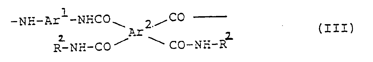
- Polyamic acid epoxy adducts I or II having the following chemical structure which are obtained, for example, by reacting a polyamic acid with a compound having at least one epoxy group: or wherein are:
- I to IV can be obtained by reacting a polyamic acid obtained by homopolymerization of an aminodicarboxylic acid derivative or reaction of a diamine with a tetracarboxylic acid derivative with an epoxy compound or an isocyanate compound.
- the tetracarboxylic acid derivative includes acid anhydrides and acid chlorides. The acid anhydrides are preferred for preparation.
- the reaction for the preparation of polyamic acids is generally carried out at -20 to 200°C in solvents such as N-methylpyrrolidone (NMP), dimethylformamide (DMF), dimethylacetamide (DMAC), dimethylsulfoxide (DMSO), dimethyl sulfate, sulforan, butyl lactone, cresol, phenol, halogenated phenols, cyclohexanone, dioxane, tetrahydrofuran, and acetophenone.
- solvents such as N-methylpyrrolidone (NMP), dimethylformamide (DMF), dimethylacetamide (DMAC), dimethylsulfoxide (DMSO), dimethyl sulfate, sulforan, butyl lactone, cresol, phenol, halogenated phenols, cyclohexanone, dioxane, tetrahydrofuran, and acetophenone.
- aminodicarboxylic acids used in the present invention mention may be made of 4-aminophthalic acid, 4-amino-5-methylphthalic acid, 4-(p-anilino)-phthalic acid, and 4-(3,5-dimethyl-4-anilino)phthalic acid, and acid anhydrides and acid chlorides thereof.
- the diamines used in the present invention include, for example, aromatic diamines such as p-phenylenediamine (p-PDA), 2,5-diaminotoluene, 2,5-diaminoxylene, diaminodurene(2,3,5,6-tetramethylphenylenediamine), 2,5-diaminobenzotrifluoride, 2,5-diaminoanisole, 2,5-diaminoacetophenone, 2,5-diaminobenzophenone, 2,5-diaminodiphenyl, 2,5-diaminofluorobenzene, benzidine, o-tolidine (o-TLD), m-tolidine, 3,3′,5,5′-tetramethylbenzidine, 3,3′-dimethoxybenzidine, 3,3′-di(trifluoromethyl)benzidine, 3,3′-diacetylbenzidine, 3,3′-difluorobenzidine, o
- diaminosiloxanes represented by the formula: wherein R5 and R7 each represents a divalent organic group, R4 and R6 each represents a monovalent organic group and p and q each denotes an integer of more than 1, may also be used as diamines.
- tetracarboxylic acids and their derivatives can be used in the present invention: Pyromellitic acid (PMDA), methylpyromellitic acid, dimethylpyromellitic acid, bis(trifluoromethyl)pyromellitic acid, 3,3′,4,4′-biphenyltetracarboxylic acid (s-BPDA), 5,5′-dimethyl-3,3′,4,4′-biphenyltetracarboxylic acid, p-(3,4-dicarboxyphenyl)-benzene, 2,3,3′,4′-tetracarboxydiphenyl, 3,3′,4,4′-tetracarboxydiphenyl ether, 2,3,3′,4′-tetracarboxydiphenyl ether, 3,3′,4,4′-tetracarboxybenzophenone (BTDA), 2,3,3′,4′-tetracarboxybenzophenone, 2,3,6,7-tetracarboxy
- the polyamic acid epoxy adducts I and II can be obtained, for example, by reacting the thus obtained polyamic acid with a compound having at least one epoxy group.
- This has the merit that polyimide precursors of high molecular weight can be prepared very easily by reaction of the polyamic acid with epoxy resins, as compared with the preparation of conventional polyamic acids by polycondensation of esterified tetracarboxylic acid and diamines using a dehydrating agent, or by converting the polyamic acid in to an acid chloride and then reacting it with an alcohol.
- the reaction of the polyamic acid with the epoxy compound can be carried out only by heating them at a temperature higher than 60°C, but in order to carry out the reaction at as low a temperature as possible without allowing imidization reaction to take place, it is preferred to use a curing accelerator for epoxy resins such as a tertiary amine, an imidazole, or triphenylphosphine as a catalyst.
- a curing accelerator for epoxy resins such as a tertiary amine, an imidazole, or triphenylphosphine
- amido polyamic acids III and IV can be obtained, for example, by reacting the polyamic acid with a compound having at least one isocyanate group. This is also easily achieved by reacting the polyamic acid with the isocyanate compound at a temperature from room temperature to about 100°C.
- the polyimide precursor V which is a reaction product of an organic diisocyanate and a tetracarboxylic acid dianhydride also has no acidic functional groups and so metal is hardly dissolved and incorporated therein and thus there is substantially no problem of deterioration of the polyimide film at high temperatures.
- the polyimide precursor films can be formed by the generally employed spin coat method and the like. In the formation of the film, it is preferred to imidize the coating by drying it at 50-250°C and then heating it to about 250-400°C.
- the adhesion of the polyimide to various substrates is important. It is preferred to roughen the surface of inorganic materials or to treat the surface with a silane coupling agent, titanate coupling agent, aluminum alcoholate, aluminum chelate, zirconium chelate, aluminum acetylacetonate, or the like. These surface treating agents may be added to the polyimide or its precursor. Alternatively, diamines or tetracarboxylic acid dianhydrides having a siloxane skeleton may be copolymerized therewith.
- the thermal expansion coefficient of the film is very small, and the modulus thereof is increased, but it is also possible to decrease the heat expansion coefficient, to increase the modulus, and to control the fluidity by incorporating therein powders, fibers, chopped strands or the like of inorganic materials, organic materials or metals.
- polyimide precursors used in the processes of the present invention in which acidic functional groups such as carboxy groups or sulfone groups are masked can be used as a conductive coating composition by adding thereto minutes of metallic materials such as a metallic powder of copper or silver.
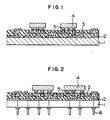
- the present invention is applied to the production of multi-chip modulus shown in Figs. 1 and 2.
- a pattern of a copper film 2 is formed on an insulating substrate or circuit board 1 by vacuum evaporation. Patterning of the copper film 2 is performed by chemical etching or dry etching which are well known in the art.
- a varnish of a precursor (i.e. a polyamic acid ester) of a polyimide is coated on the patterned copper film 2; then the coating of the precursor is dried and heated to effect imidization of the precursor.
- the polyimide film 3 is then patterned to form one or more through-holes by etching with hydrazine or by dry etching by means of an ion milling apparatus.
- Another copper film is deposited on the patterned polyimide film so that the lower copper film and upper copper film are electrically connected. Then, the upper copper film is patterned thereby to form desired circuits.
- semiconductor chips 4 are bonded to the patterned copper film through CCB 5.
- Fig. 2 shows an LSI package of ceramic pin grid array type in which the multi-layer circuit board comprising a copper film 2 and the polyimide layer 3 is produced in the same manner as in Fig. 1.
- the circuit board comprises pins 6.
- p-PDA was reacted with s-BPDA by the conventional method to obtain a 15% solution of polyamic acid in N-methyl-2-pyrrolidone (abbreviated to "NMP" hereinafter).
- NMP N-methyl-2-pyrrolidone
- the addition amount of benzyldimethylamine was 2% by weight of the phenylglycidyl ether.
- This polyamic acid epoxy adduct varnish was spin coated on to the surface of a silicon wafer having a copper thin film vapor deposited thereon to form a film of 15 »m in thickness.
- the heating conditions for imidization were heating at 100°C for 30 min, heating from 100°C to 400°C over 1 h, and keeping at that temperature for 30 min.
- the heating atmosphere was air.
- This polyimide film was peeled from the silicon wafer, and the copper content in this film, the color, the heat decomposition temperature and the tensile strength were measured. It was found that this film contained only 0.02% (atomic-absorption method) of copper, the color of the film was brown, and this was nearly the same as with a film formed on an inert SiO2 film (Comparative Example 1), the decomposition temperature in air was 505°C, the tensile strength was 400 MPa, and the elongation was 20%. This shows that this film had conspicuously excellent heat resistance and mechanical properties.
- the film was dipped in an etching solution for copper for about 5 h, and then the heat decomposition temperature and the mechanical properties were measured. It was found that the values were nearly the same as those of the film which was not dipped in the etching solution, and thus the film was chemically very stable.
- a 15% NMP solution of a polyamic acid obtained from p-PDA and s-BPDA was spin coated onto the surface of a silicon wafer provided with a silicon oxide film to form a film of a thickness of 15 »m.
- the conditions for the imidization with heating were the same as in Example 1.
- the polyimide film was peeled from the silicon wafer, and color, heat decomposition temperature and tensile strength were measured. This film had a brown color, a decomposition temperature in air of 510°C, a tensile strength of 350 MPa and an elongation of 25%, i.e., had very excellent heat resistance and mechanical properties. It can be seen that the polyimide film of Example 1 had characteristics similar to those of this film formed on an inert surface such as the thermally oxidized film. The content of copper in this film was naturally very low, namely, less than 0.0003%.
- this film was dipped in an etching solution for copper for about 5 h, and then the heat decomposition temperature and the mechanical properties of this film were measured to find that this film had nearly the same values as those of the film which was not dipped in the etching solution, and was chemically very stable as in Example 1.
- Example 2 In the same manner as in Example 1, a copper thin film was vapor deposited on a silicon wafer, a pattern was formed by etching, and thereon was coated the same polyamic acid varnish as used in Comparative Example 1 and imidized with heating under the same conditions as in Example 1. As a result, discoloration of the polyimide film on the copper pattern to blackish brown occurred, and when the film was peeled, it was torn off from the discolored portion of the copper pattern.
- copper was vapor deposited on a silicon wafer as above and then, a polyamic acid varnish was coated thereon without forming a pattern and was imidized by heating. Thereafter, it was dipped in an etching solution for copper, and the film was peeled therefrom.
- the content of copper in this film was very high, namely, 0.3%.
- This film had a heat decomposition starting temperature of 330°C and thus was inferior in heat resistance by nearly 200°C as compared with the film formed on an inert film, and besides, the film strength and elongation were much deteriorated, namely being, 150 MPa and 3%, respectively.
- These properties seem to be caused by dissolution of copper due to the presence of carboxy groups, in the polyamic acid which is a polyimide precursor and the deterioration of imide rings due to oxidation with copper in the film.
- the same polyamic acid varnish as used in Comparative Example 2 was coated on a thin copper film vapor deposited on a silicon wafer and imidized by heating in the same manner as in Comparative Example 2 except that the atmosphere for curing by heating was not air, but nitrogen gas containing a small amount of hydrogen, namely, a slightly reducing atmosphere. As a result, no change was seen in the polyimide film.
- the heat decomposition starting temperature of the polyimide film obtained by removing the copper by etching was 500°C, namely, the heat decomposition characteristic of this film, was markedly better than the film imidized by heating in air and nearly the same as the film cured on an inert film.
- film strength and elongation were 350 MPa and 21%, respectively, and were somewhat inferior as compared with those of the polyimide film formed on SiO2 film, but it was recognized that the film was subject to substantially no influence of copper. It seems that copper was dissolved due to the presence of carboxy groups in the polyamic acid which is a polyimide precursor, but the copper in the film became inert by the heat treatment in the reducing atmosphere.
- Example 2 DDE and PMDA were brought to reaction by the conventional method to obtain a 15% solution of polyamic acid in N-methyl-2-pyrrolidone (abbreviated to "NMP" hereinafter). Further, in the same manner as in Example 1, this solution was brought to reaction with an equivalent amount of phenylglycidyl ether in the presence of benzyldimethylamine at 80°C for 5 h to obtain a polyamic acid epoxy adduct. The addition amount of benzyldimethylamine was 2% by weight of the phenylglycidyl ether.
- NMP N-methyl-2-pyrrolidone
- This polyamic acid epoxy adduct varnish was spin coated on the surface of a silicon wafer having a thin copper film vapor deposited thereon to form a film of 15 »m in thickness.
- the heating conditions for imidization were heating at 100°C for 30 min, heating from 100°C to 400°C over 1 h, and keeping at that temperature for 30 min.
- the heating atmosphere was air.
- This polyimide film was peeled from the silicon wafer, and the copper content in this film, the color, the heat decomposition temperature and the tensile strength were measured.
- this film contained only 0.03% (atomic-absorption method) of copper, the color of the film was brown and this was nearly the same as with the film formed on an inert SiO2 film; the decomposition temperature in air was 460°C, the tensile strength was 180 MPa, and the elongation was 25%. This shows that this film has conspicuously excellent heat resistance and mechanical properties. These values were nearly the same as those of the film formed on an SiO2 film.
- o-TLD and BTDA were brought to reaction by the conventional method to obtain a 15% NMP solution of the polyamic acid. Furthermore, thereto was added phenyl isocyanate in an amount of 2 times the mol an amount of BDTA, and the reaction was allowed to proceed for 5 h at room temperature and for 2 h at 80°C to obtain an amido polyamic acid.
- This amido polyamic acid varnish was spin coated on the surface of a silicon wafer having a thin copper film vapor deposited thereon to form a film of 10 »m in thickness.
- the heating conditions for the imidization were the same as those in Example 1.
- This polyimide film was peeled from the silicon wafer, and the content of copper in the film, the color, the heat decomposition temperature and the tensile strength were measured.
- the film contained only 0.01% of copper and had a brown color which was nearly the same as that of the film formed on an inert SiO2 film.
- this film had markedly excellent heat resistance and mechanical properties, namely, a decomposition temperature of 430°C in air, a tensile strength of 370 MPa, and an elongation of 17%.
- Diphenylmethane diisocyanate (MDI) and s-BPDA were reacted by the conventional method to obtain a 15% NMP solution of the polyimide precursor.
- This varnish was spin coated on the surface of a silicon wafer having a thin copper film vapor deposited thereon to form a film of 15 »m in thickness. Heating for imidization was carried out in air as in Example 1.
- This polyimide film was peeled from the silicon wafer, and the content of copper in the film, the color, the heat decomposition temperature and the tensile strength were measured. As a result, the film contained only 0.015% (atomic-absorption method) of copper and had brown color which was nearly the same as that of the film formed on an inert SiO2 film. Furthermore, this film had markedly excellent heat resistance and mechanical properties, namely, a decomposition temperature of 500°C in air, a tensile strength of 330 MPa, and an elongation of 19%.
- the present invention provides a method for producing metal/polyimide composite articles according to which the oxidative deterioration of polyimide films which has been a problem when a polyamic acid is coated and cured on copper or silver can be prevented without necessity to carry out the curing in a reducing atmosphere or to use esterified polyamic acids difficult to prepare and imidized varnishes having problems in solubility.
Landscapes
- Physics & Mathematics (AREA)
- Spectroscopy & Molecular Physics (AREA)
- Chemical & Material Sciences (AREA)
- Chemical Kinetics & Catalysis (AREA)
- Engineering & Computer Science (AREA)
- Microelectronics & Electronic Packaging (AREA)
- Dispersion Chemistry (AREA)
- Macromolecular Compounds Obtained By Forming Nitrogen-Containing Linkages In General (AREA)
- Laminated Bodies (AREA)
- Polymers With Sulfur, Phosphorus Or Metals In The Main Chain (AREA)
Claims (16)
- Verfahren zur Herstellung von Kupfer- oder Silber-Polyimid-Verbundwerkstoffen, das folgende Schritte umfaßt:
Vorsehen eines Polyimid-Vorläufers im Kontakt mit Kupfer oder Silber (2) und
Erhitzen des Vorläufers, bis es sich in das Polyimid (3) umwandelt, wobei der Polyimid-Vorläufer unter Polyamidsäure-Epoxy-Addukten, Amidopolyamidsäuren und Reaktionsprodukten einer organischen Diisocyanatverbindung mit einem Tetracarbonsäuredianhydrid ausgewählt ist. - Verfahren nach Anspruch 1, wobei das Polyamidsäure-Epoxy-Addukt mindestens eine Verbindung ist, die unter den Verbindungen I und II der nachstehenden allgemeinen Formeln

 R¹ einen Rest einer Epoxyverbindung,Ar¹ einen Rest einer Diaminverbindung,Ar² einen Rest einer Tetracarbonsäure undAr³ einen Rest einer Aminodicarbonsäure.
 - Verfahren nach Anspruch 1 oder 2, wobei die Amidopolyamidsäure mindestens eine Verbindung ist, die unter den Verbindungen III und IV der nachstehenden allgemeinen Formeln

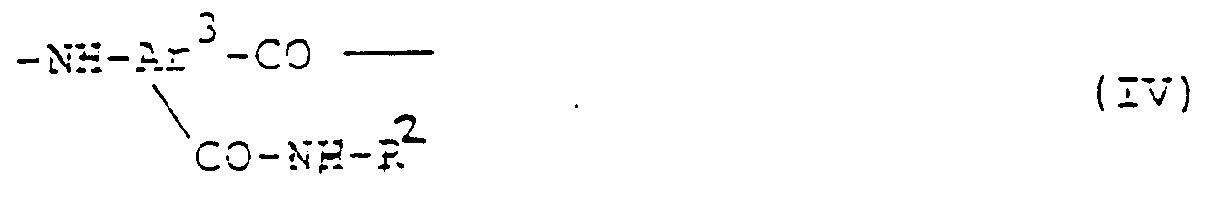
- Verfahren nach einem der Ansprüche 1 bis 3, wobei das Reaktionsprodukt eines Diisocyanats mit einem Tetracarbonsäuredianhydrid die allgemeine Formel V
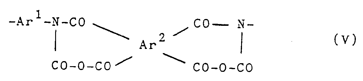 Ar² dasselbe wie in Anspruch 2 undAr¹ einen Rest eines Diisocyanatsbedeuten.
 - Verfahren zur Herstellung gedruckter Leiterplatten,
das folgende Schritte umfaßt:- Erzeugung einer dünnen Schicht aus Kupfer (2) auf einem elektrisch isolierenden Substrat (1),- Aufbringen eines Polyimid-Vorläufers auf der Schicht aus Kupfer (2) und- Erhitzen des Polyimid-Vorläufers, bis er sich in das Polyimid (3) umwandelt, wobei der eingesetzte Polyimid-Vorläufer unter Polyamidsäure-Epoxy-Addukten, Amidopolyamidsäuren und Reaktionsprodukten einer organischen Diisocyanatverbindung mit einem Tetracarbonsäuredianhydrid ausgewählt ist. - Verfahren nach Anspruch 5, wobei das Polyamidsäure-Epoxy-Addukt mindestens eine Verbindung ist, die unter den Verbindungen I und II der nachstehenden allgemeinen Formeln


worin bedeuten:R¹ einen Rest einer Epoxyverbindung,Ar¹ einen Rest einer Diaminverbindung,Ar² einen Rest einer Tetracarbonsäure undAr³ einen Rest einer Aminodicarbonsäure. - Verfahren nach Anspruch 5 oder 6, wobei die Amidopolyamidsäure mindestens eine Verbindung ist, die unter den Verbindungen III und IV der nachstehenden allgemeinen Formeln

- Verfahren nach einem der Ansprüche 5 bis 7, wobei das Reaktionsprodukt eines Diisocyanats mit einem Tetracarbonsäuredianhydrid die allgemeine Formel V
 Ar² dasselbe wie in Anspruch 6 undAr¹ einen Rest eines Diisocyanats bedeuten.
 - Verfahren zur Herstellung von Kupfer- oder Silber-Polyimid-Zusammensetzungen, das folgende Schritte umfaßt:
Vorsehen eines homogenen Gemischs aus einem Polyimid-Vorläufer, feinteiligem Kupfer oder Silber und einem organischen Lösungsmittel zum Lösen des Polyimid-Vorläufers
und
Erhitzen des Gemischs, bis sich der Polyimid-Vorläufer in das Polyimid (3) umwandelt, wobei der Polyimid-Vorläufer unter Polyamidsäure-Epoxy-Addukten, Amidopolyamidsäuren und Reaktionsprodukten einer organischen Diisocyanatverbindung mit einem Tetracarbonsäuredianhydrid ausgewählt ist. - Verfahren nach Anspruch 9, wobei das Polyamidsäure-Epoxy-Addukt mindestens eine Verbindung ist, die unter den Verbindungen I und II der nachstehenden allgemeinen Formeln


worin bedeuten:R¹ einen Rest einer Epoxyverbindung,Ar¹ einen Rest einer Diaminverbindung,Ar² einen Rest einer Tetracarbonsäure undAr³ einen Rest einer Aminodicarbonsäure. - Verfahren nach Anspruch 9 oder 10, wobei die Amidopolyamidsäure mindestens eine Verbindung ist, die unter den Verbindungen III und IV der nachstehenden allgemeinen Formeln


- Verfahren nach einem der Ansprüche 9 bis 11, wobei das Reaktionsprodukt eines Diisocyanats mit einem Tetracarbonsäuredianhydrid die allgemeine Formel V
 Ar² dasselbe wie in Anspruch 10 undAr¹ einen Rest eines Diisocyanats bedeuten.
 - Verfahren zur Herstellung von gedruckten Multilayer-Leiterplatten, das folgende Schritte umfaßt:(A) Erzeugung eines Schaltungsmusters aus einer dünnen Schicht aus Kupfer (2) auf einem elektrisch isolierenden Substrat (1),(B) Aufbringen eines Lacks aus einem Polyimid-Vorläufer auf dem Schaltungsmuster,(C) Erhitzen des Lacks, bis sich der Polyimid-Vorläufer in das Polyimid (3) umwandelt,(D) Ausbildung eines Bildmusters aus dem Polyimid (3) zur Erzeugung von Durchgangslöchern darin und(E) Erzeugung eines Schaltungsmusters aus Kupfer (2) auf dem als Bildmuster ausgebildeten Polyimid (3),wobei die Schritte B bis E wiederholt werden, bis eine erwünschte Anzahl von Schichten erhalten wird, wobei der Polyimid-Vorläufer unter Polyamidsäure-Epoxy-Addukten, Amidopolyamidsäuren und Reaktionsprodukten einer organischen Diisocyanatverbindung mit einem Tetracarbonsäuredianhydrid ausgewählt ist.
- Verfahren nach Anspruch 13, wobei das Polyamidsäure-Epoxy-Addukt mindestens eine Verbindung ist, die unter den Verbindungen I und II der nachstehenden allgemeinen Formeln

worin bedeuten:R¹ einen Rest einer Epoxyverbindung,Ar¹ einen Rest einer Diaminverbindung,Ar² einen Rest einer Tetracarbonsäure undAr³ einen Rest einer Aminodicarbonsäure. - Verfahren nach Anspruch 13 oder 14, wobei die Amidopolyamidsäure mindestens eine Verbindung ist, die unter den Verbindugnen III und IV der nachstehenden allgemeinen Formeln

- Verfahren nach einem der Ansprüche 13 bis 15, wobei das Reaktionsprodukt eines Diisocyanats mit einem Tetracarbonsäuredianhydrid die allgemeine Formel V
 Ar² dasselbe wie in Anspruch 14 undAr¹ einen Rest eines Diisocyanats bedeuten.
Applications Claiming Priority (2)
| Application Number | Priority Date | Filing Date | Title |
|---|---|---|---|
| JP243986/88 | 1988-09-30 | ||
| JP63243986A JPH07102646B2 (ja) | 1988-09-30 | 1988-09-30 | 金属とポリイミドの複合成形体 |
Publications (3)
| Publication Number | Publication Date |
|---|---|
| EP0361461A2 EP0361461A2 (de) | 1990-04-04 |
| EP0361461A3 EP0361461A3 (en) | 1990-12-19 |
| EP0361461B1 true EP0361461B1 (de) | 1995-04-26 |
Family
ID=17112011
Family Applications (1)
| Application Number | Title | Priority Date | Filing Date |
|---|---|---|---|
| EP89117907A Expired - Lifetime EP0361461B1 (de) | 1988-09-30 | 1989-09-28 | Verfahren zur Herstellung von Metall-Polyimid-Verbundwerkstoffen |
Country Status (4)
| Country | Link |
|---|---|
| US (1) | US5133989A (de) |
| EP (1) | EP0361461B1 (de) |
| JP (1) | JPH07102646B2 (de) |
| DE (1) | DE68922360T2 (de) |
Families Citing this family (13)
| Publication number | Priority date | Publication date | Assignee | Title |
|---|---|---|---|---|
| US5209814A (en) * | 1991-09-30 | 1993-05-11 | E. I. Du Pont De Nemours And Company | Method for diffusion patterning |
| WO1994018701A1 (en) * | 1993-02-05 | 1994-08-18 | W.L. Gore & Associates, Inc. | Stress-resistant semiconductor chip-circuit board interconnect |
| TW294702B (de) * | 1994-03-08 | 1997-01-01 | Sumitomo Bakelite Co | |
| KR100312150B1 (ko) * | 1994-05-17 | 2001-12-28 | 마쯔모또 에이찌 | 액정배향제및액정표시소자 |
| US5550199A (en) * | 1994-12-02 | 1996-08-27 | Exxon Research And Engineering Company | Diepoxide crosslinked/esterified polyimide-aliphatic polyester copolymers |
| US7000313B2 (en) * | 2001-03-08 | 2006-02-21 | Ppg Industries Ohio, Inc. | Process for fabricating circuit assemblies using electrodepositable dielectric coating compositions |
| US6992001B1 (en) * | 2003-05-08 | 2006-01-31 | Kulicke And Soffa Industries, Inc. | Screen print under-bump metalization (UBM) to produce low cost flip chip substrate |
| JP4923678B2 (ja) * | 2006-03-31 | 2012-04-25 | 日立化成工業株式会社 | 金属箔付フレキシブル基板及びフレキシブルプリント配線板 |
| US8999764B2 (en) * | 2007-08-10 | 2015-04-07 | International Business Machines Corporation | Ionizing radiation blocking in IC chip to reduce soft errors |
| US20090130468A1 (en) * | 2007-11-16 | 2009-05-21 | Li-Hua Wang | Polyamic acid composition, method for preparing the same, method for preparing polyimide and polyimide flexible metal-clad laminates |
| KR102068870B1 (ko) | 2016-06-17 | 2020-01-21 | 주식회사 엘지화학 | 전극 구조체, 이를 포함하는 전자 소자 및 이의 제조방법 |
| US20230025661A1 (en) * | 2021-06-25 | 2023-01-26 | Essex Furukawa Magnet Wire Usa Llc | Amine-Substituted 2-Amino-Ethan-1-Olyl Polymers, Polyimides, Articles, and Methods |
| CN114355727A (zh) * | 2022-01-17 | 2022-04-15 | 苏州理硕科技有限公司 | 一种光刻胶组合物及应用 |
Family Cites Families (21)
| Publication number | Priority date | Publication date | Assignee | Title |
|---|---|---|---|---|
| DE1570659A1 (de) * | 1964-04-15 | 1970-01-22 | Gen Electric | Polyamidsaeureharze,sowie Verfahren zu deren Herstellung |
| FR1571736A (de) * | 1967-06-26 | 1969-06-20 | ||
| CH549069A (de) * | 1971-02-26 | 1974-05-15 | Ciba Geigy Ag | Verfahren zur herstellung von in organischen loesungsmitteln loeslichen, n-silylgruppenhaltigen polymeren. |
| JPS5545746A (en) * | 1978-09-29 | 1980-03-31 | Hitachi Ltd | Reactive polymer composition |
| JPS55135124A (en) * | 1979-04-10 | 1980-10-21 | Hitachi Chem Co Ltd | Production of polyimide-amide carboxylic acid |
| EP0019391B1 (de) * | 1979-05-12 | 1982-10-06 | Fujitsu Limited | Verfahren zur Herstellung einer elektronischen Vorrichtung mit Vielschicht-Verdrahtungsstruktur |
| JPS5888741A (ja) * | 1981-11-20 | 1983-05-26 | Hitachi Chem Co Ltd | 感光性樹脂組成物及び感光性樹脂組成物積層体 |
| JPS5968332A (ja) * | 1982-10-13 | 1984-04-18 | Nitto Electric Ind Co Ltd | 感光性樹脂組成物 |
| EP0116297B1 (de) * | 1983-01-15 | 1987-12-02 | Akzo GmbH | Polyimid-Laminate mit hoher Schälfestigkeit und Verfahren zu deren Herstellung |
| US4648179A (en) * | 1983-06-30 | 1987-03-10 | International Business Machines Corporation | Process of making interconnection structure for semiconductor device |
| DE3486131T2 (de) * | 1983-08-01 | 1993-10-28 | Hitachi Chemical Co Ltd | Harzmaterial mit geringer thermischer Ausdehnung für Verdrahtungsisolationsfolie. |
| KR850002551A (ko) * | 1983-09-30 | 1985-05-13 | 원본미기재 | 두꺼운 니켈 폴리머필름 |
| US4654223A (en) * | 1983-11-30 | 1987-03-31 | International Business Machines Corporation | Method for forming a film of dielectric material on an electric component |
| US4699803A (en) * | 1983-11-30 | 1987-10-13 | International Business Machines Corporation | Method for forming electrical components comprising cured vinyl and/or acetylene terminated copolymers |
| US4656050A (en) * | 1983-11-30 | 1987-04-07 | International Business Machines Corporation | Method of producing electronic components utilizing cured vinyl and/or acetylene terminated copolymers |
| JPS60206639A (ja) * | 1984-03-31 | 1985-10-18 | 日東電工株式会社 | ポリイミド−金属箔複合フイルムの製造方法 |
| US4758476A (en) * | 1984-12-12 | 1988-07-19 | Hitachi Chemical Company, Ltd. | Polyimide precursor resin composition and semiconductor device using the same |
| CA1290490C (en) * | 1985-11-20 | 1991-10-08 | Masakazu Uekita | Amphiphilic high polymer and process for producing the same |
| CA1294731C (en) * | 1986-04-25 | 1992-01-21 | Masakazu Uekita | Copolymeric and amphiphilic polyimide precursor, process for preparing the same and thin film |
| US4943471A (en) * | 1986-05-20 | 1990-07-24 | Kanegafuchi Kagaku Kogyo Kabushiki Kaisha | Patterned thin film and process for preparing the same |
| JPH0727966B2 (ja) * | 1986-07-04 | 1995-03-29 | 日立化成工業株式会社 | 半導体装置 |
-
1988
- 1988-09-30 JP JP63243986A patent/JPH07102646B2/ja not_active Expired - Lifetime
-
1989
- 1989-09-27 US US07/416,279 patent/US5133989A/en not_active Expired - Fee Related
- 1989-09-28 EP EP89117907A patent/EP0361461B1/de not_active Expired - Lifetime
- 1989-09-28 DE DE68922360T patent/DE68922360T2/de not_active Expired - Fee Related
Non-Patent Citations (1)
| Title |
|---|
| PATENT ABSTRACT OF JAPAN, vol.12, no. 70 (C-479) (2917), 4th March 1988; & JP-A-62 207 331. * |
Also Published As
| Publication number | Publication date |
|---|---|
| DE68922360T2 (de) | 1995-09-28 |
| EP0361461A3 (en) | 1990-12-19 |
| EP0361461A2 (de) | 1990-04-04 |
| JPH0292535A (ja) | 1990-04-03 |
| DE68922360D1 (de) | 1995-06-01 |
| JPH07102646B2 (ja) | 1995-11-08 |
| US5133989A (en) | 1992-07-28 |
Similar Documents
| Publication | Publication Date | Title |
|---|---|---|
| EP0133533B1 (de) | Harzmaterial mit geringer thermischer Ausdehnung für Verdrahtungsisolationsfolie | |
| EP1448669B1 (de) | Bindemittel enthaltend ein polyimidcopolymer und verfahren zu dessen herstellung | |
| EP0361461B1 (de) | Verfahren zur Herstellung von Metall-Polyimid-Verbundwerkstoffen | |
| JPH10182820A (ja) | ポリイミド前駆体組成物及びポリイミド膜 | |
| KR960007934B1 (ko) | 저-열팽창성 수지 | |
| JPH04262593A (ja) | 多層配線構造体およびその製造方法とその用途 | |
| JPH0740629B2 (ja) | 電子装置用多層配線基板の製法 | |
| JP4008249B2 (ja) | 絶縁樹脂組成物及び絶縁樹脂シート並びにプリント配線板 | |
| EP0361462B1 (de) | Verfahren zur Herstellung eines aus Kupfer oder Silber/Polyimid zusammengesetzten Artikels | |
| EP1494247B1 (de) | Polyimidmassen für elektrische Isolation | |
| KR100820221B1 (ko) | 플렉시블프린트 배선판용 기판의 제조방법 및플렉시블프린트 배선판용 기판 | |
| JP3653499B2 (ja) | ポリ(イミド−ベンゾオキサゾール)コポリマー | |
| US5734008A (en) | Polyimide film | |
| KR20110035620A (ko) | 폴리이미드 필름 | |
| JPWO2001097578A1 (ja) | フレキシブルプリント配線板用基板の製造方法及びフレキシブルプリント配線板用基板 | |
| JP3072704B2 (ja) | ポリ(アリールエーテルベンズイミダゾール)およびそれを適用した電子パッケージ | |
| WO2008073410A2 (en) | Crystalline encapsulants | |
| JP3079740B2 (ja) | ポリイミド及びそれを用いた配線構造体 | |
| US20020076535A1 (en) | Thermosetting fluorinated dielectrics and multilayer circuit boards | |
| JPH02167741A (ja) | 金属/ポリイミド複合体の製造方法 | |
| JPH0532891A (ja) | 熱硬化性樹脂組成物およびそれを用いたプリント配線板 | |
| JP3602206B2 (ja) | 配線構造体とその製造法 | |
| JPH024631B2 (de) | ||
| JP2006269558A (ja) | フレキシブル積層基板の製造方法 | |
| JP3065388B2 (ja) | フレキシブル印刷回路板の製造方法 |
Legal Events
| Date | Code | Title | Description |
|---|---|---|---|
| PUAI | Public reference made under article 153(3) epc to a published international application that has entered the european phase |
Free format text: ORIGINAL CODE: 0009012 |
|
| AK | Designated contracting states |
Kind code of ref document: A2 Designated state(s): CH DE FR GB LI NL SE |
|
| PUAL | Search report despatched |
Free format text: ORIGINAL CODE: 0009013 |
|
| AK | Designated contracting states |
Kind code of ref document: A3 Designated state(s): CH DE FR GB LI NL SE |
|
| 17P | Request for examination filed |
Effective date: 19901113 |
|
| 17Q | First examination report despatched |
Effective date: 19920224 |
|
| GRAA | (expected) grant |
Free format text: ORIGINAL CODE: 0009210 |
|
| AK | Designated contracting states |
Kind code of ref document: B1 Designated state(s): CH DE FR GB LI NL SE |
|
| REF | Corresponds to: |
Ref document number: 68922360 Country of ref document: DE Date of ref document: 19950601 |
|
| ET | Fr: translation filed | ||
| PLBE | No opposition filed within time limit |
Free format text: ORIGINAL CODE: 0009261 |
|
| STAA | Information on the status of an ep patent application or granted ep patent |
Free format text: STATUS: NO OPPOSITION FILED WITHIN TIME LIMIT |
|
| 26N | No opposition filed | ||
| PGFP | Annual fee paid to national office [announced via postgrant information from national office to epo] |
Ref country code: SE Payment date: 19980624 Year of fee payment: 10 |
|
| PGFP | Annual fee paid to national office [announced via postgrant information from national office to epo] |
Ref country code: CH Payment date: 19990622 Year of fee payment: 11 |
|
| PG25 | Lapsed in a contracting state [announced via postgrant information from national office to epo] |
Ref country code: SE Free format text: THE PATENT HAS BEEN ANNULLED BY A DECISION OF A NATIONAL AUTHORITY Effective date: 19990929 |
|
| EUG | Se: european patent has lapsed |
Ref document number: 89117907.9 |
|
| PG25 | Lapsed in a contracting state [announced via postgrant information from national office to epo] |
Ref country code: LI Free format text: LAPSE BECAUSE OF NON-PAYMENT OF DUE FEES Effective date: 20000930 Ref country code: CH Free format text: LAPSE BECAUSE OF NON-PAYMENT OF DUE FEES Effective date: 20000930 |
|
| REG | Reference to a national code |
Ref country code: CH Ref legal event code: PL |
|
| PGFP | Annual fee paid to national office [announced via postgrant information from national office to epo] |
Ref country code: FR Payment date: 20010823 Year of fee payment: 13 |
|
| PGFP | Annual fee paid to national office [announced via postgrant information from national office to epo] |
Ref country code: NL Payment date: 20010828 Year of fee payment: 13 Ref country code: GB Payment date: 20010828 Year of fee payment: 13 |
|
| PGFP | Annual fee paid to national office [announced via postgrant information from national office to epo] |
Ref country code: DE Payment date: 20010928 Year of fee payment: 13 |
|
| REG | Reference to a national code |
Ref country code: GB Ref legal event code: IF02 |
|
| PG25 | Lapsed in a contracting state [announced via postgrant information from national office to epo] |
Ref country code: GB Free format text: LAPSE BECAUSE OF NON-PAYMENT OF DUE FEES Effective date: 20020928 |
|
| PG25 | Lapsed in a contracting state [announced via postgrant information from national office to epo] |
Ref country code: NL Free format text: LAPSE BECAUSE OF NON-PAYMENT OF DUE FEES Effective date: 20030401 Ref country code: DE Free format text: LAPSE BECAUSE OF NON-PAYMENT OF DUE FEES Effective date: 20030401 |
|
| GBPC | Gb: european patent ceased through non-payment of renewal fee |
Effective date: 20020928 |
|
| PG25 | Lapsed in a contracting state [announced via postgrant information from national office to epo] |
Ref country code: FR Free format text: LAPSE BECAUSE OF NON-PAYMENT OF DUE FEES Effective date: 20030603 |
|
| REG | Reference to a national code |
Ref country code: FR Ref legal event code: ST |