EP0361807A2 - Bit-Schieberegisteranordnung - Google Patents
Bit-Schieberegisteranordnung Download PDFInfo
- Publication number
- EP0361807A2 EP0361807A2 EP89309676A EP89309676A EP0361807A2 EP 0361807 A2 EP0361807 A2 EP 0361807A2 EP 89309676 A EP89309676 A EP 89309676A EP 89309676 A EP89309676 A EP 89309676A EP 0361807 A2 EP0361807 A2 EP 0361807A2
- Authority
- EP
- European Patent Office
- Prior art keywords
- source
- gate
- module
- drain
- transistor
- Prior art date
- Legal status (The legal status is an assumption and is not a legal conclusion. Google has not performed a legal analysis and makes no representation as to the accuracy of the status listed.)
- Ceased
Links
- 230000015572 biosynthetic process Effects 0.000 abstract 1
- 102100040862 Dual specificity protein kinase CLK1 Human genes 0.000 description 16
- 101000749294 Homo sapiens Dual specificity protein kinase CLK1 Proteins 0.000 description 14
- 102100040844 Dual specificity protein kinase CLK2 Human genes 0.000 description 5
- 101000749291 Homo sapiens Dual specificity protein kinase CLK2 Proteins 0.000 description 5
- 101150110971 CIN7 gene Proteins 0.000 description 2
- 101100286980 Daucus carota INV2 gene Proteins 0.000 description 2
- 101150110298 INV1 gene Proteins 0.000 description 2
- 101100397044 Xenopus laevis invs-a gene Proteins 0.000 description 2
- 101100397045 Xenopus laevis invs-b gene Proteins 0.000 description 2
- 230000008901 benefit Effects 0.000 description 2
- 239000003990 capacitor Substances 0.000 description 2
- 238000001208 nuclear magnetic resonance pulse sequence Methods 0.000 description 2
- 230000000630 rising effect Effects 0.000 description 2
- 230000000295 complement effect Effects 0.000 description 1
- 238000010586 diagram Methods 0.000 description 1
- 230000009977 dual effect Effects 0.000 description 1
- 230000004048 modification Effects 0.000 description 1
- 238000012986 modification Methods 0.000 description 1
- 239000004065 semiconductor Substances 0.000 description 1
Images

Classifications
-
- G—PHYSICS
- G11—INFORMATION STORAGE
- G11C—STATIC STORES
- G11C19/00—Digital stores in which the information is moved stepwise, e.g. shift registers
- G11C19/18—Digital stores in which the information is moved stepwise, e.g. shift registers using capacitors as main elements of the stages
- G11C19/182—Digital stores in which the information is moved stepwise, e.g. shift registers using capacitors as main elements of the stages in combination with semiconductor elements, e.g. bipolar transistors, diodes
- G11C19/184—Digital stores in which the information is moved stepwise, e.g. shift registers using capacitors as main elements of the stages in combination with semiconductor elements, e.g. bipolar transistors, diodes with field-effect transistors, e.g. MOS-FET
Definitions
- This invention relates to shift registers in a computer for forming and holding data bits.
- Dynamic shift registers are used in computers for a variety of purposes.
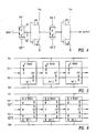
- Figure 1 shows one well known logic diagram for a dynamic shift register bit.
- a data bit appears at the input terminal and is blocked by a first data passage control means or transfer gate T1 until T1 senses the next rising edge or next falling edge of a clock pulse CLK1 received thereat.
- the electric charge associated with the data bit held at T1 is stored in a capacitor such as C1.
- T1 When T1 allows passage of the data bit (conventionally assumed to be a "0" or a "1"), this bit is logically inverted by a first inverter INV1 and passed to a second bit passage control means or transfer gate T2, which allows passage of the bit only upon receipt thereafter of a rising edge or a falling edge of a second independent clock pulse CLK2.
- the electric charge associated with the bit held at T2 is stored in a capacitor such as C2; and when T2 releases the bit for passage, the bit is again logically inverted by an inverter INV2 so that the data bit appearing at the output is substantially the same as the data bit appearing at the input.
- the two clock pulses received from clock pulse sources CLK1 and CLK2 received at bit passage control means T1 and T2, respectively, are drawn from independent clock pulse sequences as shown in Figure 2, the only constraint being that between any two consecutive pulses of CLK1 a single pulse of CLK2 must appear, and conversely.
- the clock pulses associated with CLK1 and CLK2 are to be nonoverlapping.
- the two-phase shift register shown schematically in Figure 1 has been used throughout the industry for more than twenty years. After one pulse from CLK1 and one pulse from CLK2, the data bit that appeared earlier at the input terminal will appear at the output terminal of this device.
- FIG 3 shows a common implementation of the two-phase dynamic shift register using n-channel conductivity type MOS transistors T1-T6 for this purpose.
- Transistors T1 and T4 serve as the transfer gates, TG1 and TG2, respectively, in Figure 1; transistors T2 and T3 together comprise the inverter INV1; and transistors T5 and T6 together comprise the inverter INV2. Note that each data bit processed requires six transistors and delivery of two clock pulses.
- Figure 4 illustrates a common CMOS implementation for a two-phase shift register that has the inherent benefit that it requires no additional standby power.
- An n-channel CMOS transistor T1 and a p-channel CMOS transistor T2 are connected drain-to-drain and source-to-source as shown, and the gates G1′ and G2′ of these two transistors receive complementary clock pulses CLK and CLK*.
- the transfer gate T2′ transfers a true “1” irrespective of the value of this data bit transferred by transfer gate T1′; the data bit "1" will, of course, be transferred at different times by the gates T1′ and T2′.
- transfer gate T1′ When a "0" data bit arrives at the input terminal, transfer gate T1′ will transfer a true “0” bit irrespective of the reduced value transferred by transfer gate T2′, again at slightly different times.
- the result of this configuration is that the data bit that arrives at the common source S′ shown in Figure 4 is a true “0” data bit or a true “1” data bit, and no increase in standby power is required to preserve noise margins.
- a similar result occurs at the combination of transfer gates T5′ and T6′ shown in Figure 4.
- Figure 4 requires eight CMOS transistors and delivery of four different clock phase signals and thus requires more semiconductor real estate than the simpler configuration shown in Figure 3.
- Figures 5 and 6 compare schematically the requirements of the simpler n-channel system indicated in Figure 3 with the more complex CMOS configuration required by Figure 4.
- One embodiment of the invention may include: a first module having a data input terminal, a clock input terminal, a power supply terminal and a data output terminal and comprising: a first MOS transistor having a drain, a gate and a source, with the drain being connected to the module input terminal and the gate being connected tothe clock input terminal; an array of MOStransistors comprising at least a second MOS transistor of n-channel conductivity type and a third MOS transistor of p-channel conductivity type, with the gates of the second and third MOS transistors of this array each being connected to the source of the first transistor, with the sources of the second and third transistors each being connected to the outpout terminal of the first module, with the drain of the second transistor being connected to the ground terminal and with the drain of the third transistor being connected to the power supply terminal; where this array provides a gate voltage at the gates of the second and third transistors that is substantially equal to the voltage at the power supply terminal when the gate of the first transistor passes a signal voltage that is higher than a predetermined voltage, and
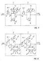
- FIG. 7 shows one preferred embodiment of the invention.
- an NMOS transistor T1 ⁇ has its drain connected to the device input terminal and its gate driven by a clock phase source CLK1.
- the source S1 ⁇ of NMOS transistor T1 ⁇ is connected to the gate G2 ⁇ of an NMOS transistor T2 ⁇ whose drain D2 ⁇ is connected to ground, and is connected to the gate G3 ⁇ of a PMOS transistor T3 ⁇ whose drain is connected to a power supply V cc .
- the sources S2 ⁇ and S3 ⁇ of the transistors T2 ⁇ and T3 ⁇ , respectively, are both connected to the gate G7 ⁇ of a PMOS transistor T7 ⁇ whose drain is also connected to the power supply V cc .
- the source of transistor T7 ⁇ is connected to the source of transistor T1 ⁇ .
- the module 11 comprising an input terminal for the clock phase source CLK1, the data input terminal, and the four transistors T1 ⁇ , T2 ⁇ , T3 ⁇ and T7 ⁇ produces an output signal at the point denoted INT, and the output signal of the module 11 serves as the (intermediate) data input signal for the module 13, which is configured identically to module 11.
- Each of modules 11 and 13 comprises one phase of a two-phase shift register here.
- the source and drain of any transistor shown in any of Figures 7-10 are interchangeable here.
- module 11 With the p-channel transistor T7 ⁇ removed therefrom. If a "1" data bit arrives at the input terminal for module 11, the next clock pulse from clock phase source CLK1 will produce a "1" at the source of transistor T1 ⁇ , and this "1" data bit will also appear at the gates of transistors T2 ⁇ and T3 ⁇ . This will turn transistor T2 ⁇ on so that the voltage at the source of transistor T2 ⁇ will be substantially zero. Appearance of a "1" data bit at the gate of PMOS transistor T3 ⁇ will leave the gate closed so that the voltage at the source of transistor T3 ⁇ will be whatever is the source voltage appearing at transistor T2 ⁇ to which it is connected. This configuration, by itself, may experience the previously-discussed problem that a true "1" data bit may not appear at the source of transistor T1 ⁇ .
- the PMOS transistor T7 ⁇ is included in the module 11 as shown.
- the next clock pulse from the clock phase source CLK1 will transfer the "1" data bit to the gates G2 ⁇ and G3 ⁇ of NMOS transistor T2 ⁇ and PMOS transistor T3 ⁇ , respectively, as before.
- the next clock pulse from the clock phase source CLK1 will, as before, produce a logical "0" at the gates of transistors T2 ⁇ and T3 ⁇ ; this will open gate T3 ⁇ so that the voltage at the source of T3 ⁇ becomes substantially the voltage of the power supply V cc .
- the voltage at the gate G7 ⁇ of transistor T7 ⁇ also becomes substantially the power supply voltage, and the gate G7 ⁇ remains closed so that a logical "0" that appears at the source S1 ⁇ of transistor T1 ⁇ is undisturbed.
- the signal that appears at the output terminal INT for the module 11 is then a logical "1" as desired.
- the module 13 operates in an analogous manner.
- Figure 8 illustrates a second preferred embodiment of the invention, wherein the NMOS transistors T2 ⁇ and T5 ⁇ are replaced by PMOS transistors T2′′′ and T5′′′, respectively, and the drain connections to ground of T2 ⁇ and T5 ⁇ are replaced by connections to the power supply terminal, which may be held at a voltage V cc ; and the PMOS transistor T3 ⁇ , T6 ⁇ , T7 ⁇ and T8 ⁇ are replaced by NMOS transistors T3′′′, T6′′′, T7′′′, and T8′′′, respectively, and the respective connections to the power supply terminal are replaced by connections to a ground terminal for each of these four NMOS transistors. Analysis of operation of the circuit shown in Figure 8 proceeds as before.
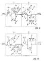
- Figure 9 illustrates a third preferred embodiment in which the modules 11 and 17 from Figures 7 and 8, respectively, are connected to produce a similar result
- Figure 10 illustrates a fourth preferred embodiment in which the modules 15 and 13 from Figures 8 and 7, respectively, are connected as shown to produce a similar result.
- modules 11 and 15 in Figures 7 and 8 are duals of one another in a certain sense: if each NMOS transistor and its associated external supply drain voltage (at the ground terminal) is replaced by a PMOS transistor and its associated external supply drain voltage (at the power supply terminal), and each PMOS transistor and its associated external supply drain voltage is replaced by an NMOS transistor and its associated external supply drain voltage, ignoring the input transistors T1 ⁇ and T1′′′, the modules 11 and 15 are transformed into one another.
Landscapes
- Engineering & Computer Science (AREA)
- Microelectronics & Electronic Packaging (AREA)
- Power Engineering (AREA)
- Static Random-Access Memory (AREA)
- Logic Circuits (AREA)
- Shift Register Type Memory (AREA)
Applications Claiming Priority (2)
| Application Number | Priority Date | Filing Date | Title |
|---|---|---|---|
| US25172588A | 1988-09-30 | 1988-09-30 | |
| US251725 | 1988-09-30 |
Publications (2)
| Publication Number | Publication Date |
|---|---|
| EP0361807A2 true EP0361807A2 (de) | 1990-04-04 |
| EP0361807A3 EP0361807A3 (de) | 1990-10-17 |
Family
ID=22953144
Family Applications (1)
| Application Number | Title | Priority Date | Filing Date |
|---|---|---|---|
| EP19890309676 Ceased EP0361807A3 (de) | 1988-09-30 | 1989-09-22 | Bit-Schieberegisteranordnung |
Country Status (2)
| Country | Link |
|---|---|
| EP (1) | EP0361807A3 (de) |
| JP (1) | JPH02122499A (de) |
Cited By (2)
| Publication number | Priority date | Publication date | Assignee | Title |
|---|---|---|---|---|
| US5448194A (en) * | 1992-02-21 | 1995-09-05 | Siemens Aktiengesellschaft | Circuit for the buffer storage of a bit, and use of the circuit as an address buffer store |
| WO2026040041A1 (zh) * | 2024-08-22 | 2026-02-26 | 京东方科技集团股份有限公司 | 移位寄存器单元及其驱动方法、显示驱动电路、显示装置 |
Family Cites Families (3)
| Publication number | Priority date | Publication date | Assignee | Title |
|---|---|---|---|---|
| GB1113111A (en) * | 1964-05-29 | 1968-05-08 | Nat Res Dev | Digital storage devices |
| JPS4897468A (de) * | 1972-03-27 | 1973-12-12 | ||
| US4733111A (en) * | 1985-07-17 | 1988-03-22 | CSELT--Centro Studi e Laboratori Telecomunicazioni S.p.A. | Sequential-logic basic element in CMOS technology operating by a single clock signal |
-
1989
- 1989-09-22 EP EP19890309676 patent/EP0361807A3/de not_active Ceased
- 1989-09-28 JP JP1253726A patent/JPH02122499A/ja active Pending
Cited By (2)
| Publication number | Priority date | Publication date | Assignee | Title |
|---|---|---|---|---|
| US5448194A (en) * | 1992-02-21 | 1995-09-05 | Siemens Aktiengesellschaft | Circuit for the buffer storage of a bit, and use of the circuit as an address buffer store |
| WO2026040041A1 (zh) * | 2024-08-22 | 2026-02-26 | 京东方科技集团股份有限公司 | 移位寄存器单元及其驱动方法、显示驱动电路、显示装置 |
Also Published As
| Publication number | Publication date |
|---|---|
| EP0361807A3 (de) | 1990-10-17 |
| JPH02122499A (ja) | 1990-05-10 |
Similar Documents
| Publication | Publication Date | Title |
|---|---|---|
| US5576645A (en) | Sample and hold flip-flop for CMOS logic | |
| KR100239099B1 (ko) | 전자 플립-플롭 회로 | |
| US5852373A (en) | Static-dynamic logic circuit | |
| US5550490A (en) | Single-rail self-resetting logic circuitry | |
| EP0606912B1 (de) | CMOS Schaltungen zur Erzeugung mehrphasiger Taktsignalen | |
| US5087835A (en) | Positive edge triggered synchronized pulse generator | |
| JPH05276016A (ja) | ランダム論理適用のための動的レイショレス・サーキットリー | |
| JPH11167791A (ja) | 高速非同期パイプライン制御回路及び高速非同期向流パイプライン制御回路並びに、これに用いられるコンピュータメモリ | |
| US6060909A (en) | Compound domino logic circuit including an output driver section with a latch | |
| US5936449A (en) | Dynamic CMOS register with a self-tracking clock | |
| US4985905A (en) | Two phase CMOS shift register bit for optimum power dissipation | |
| US4570085A (en) | Self booting logical AND circuit | |
| JPH03192915A (ja) | フリップフロップ | |
| EP0361807A2 (de) | Bit-Schieberegisteranordnung | |
| JP3151329B2 (ja) | データ出力回路 | |
| JP3699674B2 (ja) | 信号伝送回路、固体撮像装置、カメラおよび表示装置 | |
| EP0664614B1 (de) | Gegenüber einer Versorgungsspannungsschwankung unempfindliche Dekodierschaltung | |
| US5917367A (en) | Power supply solution for mixed signal circuits | |
| KR20000069742A (ko) | 처음과 마지막 스테이지에는 클록을 그리고 마지막 스테이지에는 래치를 구비한 단일-위상 도미노 시간 빌림 논리 | |
| JP4386523B2 (ja) | ダイナミック論理回路 | |
| US3657570A (en) | Ratioless flip-flop | |
| JPS63155822A (ja) | Mos論理回路 | |
| KR100424957B1 (ko) | 반도체 집적회로 장치 | |
| JPH0377599B2 (de) | ||
| JP2690604B2 (ja) | 半導体集積回路 |
Legal Events
| Date | Code | Title | Description |
|---|---|---|---|
| PUAI | Public reference made under article 153(3) epc to a published international application that has entered the european phase |
Free format text: ORIGINAL CODE: 0009012 |
|
| AK | Designated contracting states |
Kind code of ref document: A2 Designated state(s): AT BE CH DE ES FR GB GR IT LI LU NL SE |
|
| PUAL | Search report despatched |
Free format text: ORIGINAL CODE: 0009013 |
|
| AK | Designated contracting states |
Kind code of ref document: A3 Designated state(s): AT BE CH DE ES FR GB GR IT LI LU NL SE |
|
| 17P | Request for examination filed |
Effective date: 19901217 |
|
| 17Q | First examination report despatched |
Effective date: 19930518 |
|
| STAA | Information on the status of an ep patent application or granted ep patent |
Free format text: STATUS: THE APPLICATION HAS BEEN REFUSED |
|
| 18R | Application refused |
Effective date: 19950403 |