EP0361887A2 - Multiprozessor/Cache-Speicheranordnung und Datenvorgangssteuerung dafür - Google Patents
Multiprozessor/Cache-Speicheranordnung und Datenvorgangssteuerung dafür Download PDFInfo
- Publication number
- EP0361887A2 EP0361887A2 EP89309827A EP89309827A EP0361887A2 EP 0361887 A2 EP0361887 A2 EP 0361887A2 EP 89309827 A EP89309827 A EP 89309827A EP 89309827 A EP89309827 A EP 89309827A EP 0361887 A2 EP0361887 A2 EP 0361887A2
- Authority
- EP
- European Patent Office
- Prior art keywords
- cache
- data
- bus
- main memory
- memory
- Prior art date
- Legal status (The legal status is an assumption and is not a legal conclusion. Google has not performed a legal analysis and makes no representation as to the accuracy of the status listed.)
- Withdrawn
Links
Images




Classifications
-
- G—PHYSICS
- G06—COMPUTING OR CALCULATING; COUNTING
- G06F—ELECTRIC DIGITAL DATA PROCESSING
- G06F12/00—Accessing, addressing or allocating within memory systems or architectures
- G06F12/02—Addressing or allocation; Relocation
- G06F12/08—Addressing or allocation; Relocation in hierarchically structured memory systems, e.g. virtual memory systems
- G06F12/0802—Addressing of a memory level in which the access to the desired data or data block requires associative addressing means, e.g. caches
- G06F12/0806—Multiuser, multiprocessor or multiprocessing cache systems
- G06F12/0815—Cache consistency protocols
- G06F12/0831—Cache consistency protocols using a bus scheme, e.g. with bus monitoring or watching means
- G06F12/0833—Cache consistency protocols using a bus scheme, e.g. with bus monitoring or watching means in combination with broadcast means (e.g. for invalidation or updating)
Definitions
- This invention relates generally to data processing systems using multiple processors each having an associated cache memory and, more particularly, to techniques for efficiently handling the simultaneous transfer of different data to different cache memories and the accessing and transfer of modified data simultaneously to main memory and to a requesting cache memory in a coherent manner.
- control system controls the selection of which data is to be transferred on which bus and in each case controllably directs particular data to a particular cache unit which is requesting it on a particular bus which is selected for that purpose.
- modified data i.e., data which has been modified by one of the processors during a processing operation.
- the system normally stores the modified data in the modifying processor's cache memory but does not immediately provide the modified data either to main memory or to any other cache memory of the system which may request it.
- the modified data is then subsequently copied into main memory and into such other cache memory which has requested it.
- the subsequent copying operation requires an extra data transfer cycle and, accordingly, increases the overall operating time for the system in performing such transfer operation.
- the modified data is stored in main memory only and subsequently the data is accessed from main memory and copied into the requesting cache memory. Again, such operation requires an additional data transfer cycle.
- the system must assure that the modified data is correctly identified, i.e., by its correct address, sometimes referred to as an address coherency requirement.
- each of a plurality of cache memory units is ported to each of a plurality of buses.
- Different data can be separately broadcast simultaneously each different data being broadcast on a different bus, all of the broadcasted data thereby being available to each cache unit via the different buses to which cache is ported.
- Each cache unit thereupon identifies which data, if any, is intended to be transferred to it. Data identified as intended for a particular cache unit is then accepted by the intended cache from the bus on which that data resides and is being transferred and all other data, not intended for that particular cache unit, can be ignored by it. In this manner, different data can be simultaneously transferred or broadcast on a different one of the plurality of buses and accepted only by those cache units for which each different data is intended.
- the transfer of modified data from one cache to another cache which has requested the modified data and the copying back of the modified data to main memory are optimized by arranging for an immediate transfer of the modified data to main memory simultaneously with the cache-to-cache transfer.
- Such operation can be provided in a multiple processor/multiple cache system using a control led cache unit bus and a controlled main memory bus, transactions being capable of occurring simultaneously on such busses to permit communication with the requesting cache unit and with the main memory simultaneously. If multiple cache unit buses and main memory buses are used, independent processing operations can be performed on the other sets of cache unit/main memory buses at the same time the modified data transfer occurs.
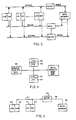
- memory control unit 14 controls the broadcasting of the data from cache unit 12 onto cache unit bus 16
- memory control 15 controls the simultaneous broadcasting of the data from cache unit 13 onto cache unit bus 17.
- the destination for data is implicit in the bus protocol (see discussion thereof below), i.e., if a unit requests data, the next data placed on the bus is autpmatically the data intended for that requestor.
- the cache unit When a particular cache unit receives the data which has been broadcast on any cache bus as destined for it, the cache unit includes additional logic for receiving and appropriately storing such data therein. Such operation is illustrated by the timing diagram shown in Fig.2 and is further discussed later with respect to the bus protocol discussed below.
- processor J0 ⁇ ...JPN and cache units DC0 ⁇ ...DCN in Fig. 3 each of the cache units are ported to each of a plurality of N cache unit buses as shown by MCB0 ⁇ ...MCBN.
- Control of data accessing and transfer is provided by N memory control units MCU0 ⁇ ... MCUN, each controlling the use of a corresponding pair of cache unit bus as well main memory buses, MMB0 ⁇ ...MMBN, for such purpose.
- each cache unit can broadcast data identified as destined for another cache unit onto a selected cache unit bus under control of the memory control unit which controls such bus. For example, if, full capability of the broadcast scheme is required, each of the N cache units may be required to transfer data to one of the other cache units.
- Such different data transfer can be performed simultaneously such that each cache unit broadcasts its data on a different one of the cache buses simultaneously with the broadcasting of data by each of the other cache unit on the other cache buses.
- Each cache unit accepts only the data which is destined for it and thereupon receives and stores such data simultaneously with the receiving and storing of the other data by other cache units.
- Fig. 4 provides a block diagram for illustrating another common problem which arises in multiple processor/multiple cache memory systems for handing transfers of modified data.
- the system is shown as using two processors (JP0 ⁇ and JP1) 30 and 31, each of which has associated with it a cache memory unit (DC0 ⁇ and DC1) 32 and 33, respectively.
- a management control unit (MCU) 34 controls data transfer operations among the processor units, the cache units, and a main memory unit (MMU) 35 via a bus 36.
- processor 30 has requested data D0 ⁇ from main memory 35, has accessed such data and has placed it into its cache unit 32.
- processor 30 modifies the data, which data can be referred to as modified data D1.
- Processor 31 thereupon requests the modified data to be placed into its cache unit 33.
- a copy of modified data D1 must also be written into main memory 35 identifiable by the same address therein as that of the original unmodified data D0 ⁇ .
- JP0 ⁇ accesses data D0 ⁇ , modifies it to data D1, and then places D1 into its cache unit DC0 ⁇ .
- the modified data is then subsequently written into main memory at the same address as the original data D0 ⁇ .
- JP1 then subsequently reads the modified data D1 from main memory and places it into its cache unit DC1.
- Such operation requires in effect two data transfers, once the data has been modified.
- JP0 ⁇ accesses data D0 ⁇ , modifies it to D1 and places D1 into its cache unit CU0 ⁇ . D1 is then transferred from cache unit DC0 ⁇ into cache unit DC1 at the request of processor JP1. JP1 uses modified data D1 and then subsequently transfers D1 to the address in main memory of original data D0 ⁇ . Such operation also requires in effect two data transfer operations once the data has been modified.
- the system of the invention is arranged as shown in FIG. 5.
- a dual processor/dual cache memory system comprises a first processor (JP) 30 and an associated cache memory unit (DC0 ⁇ ) 32 and a second processor (JP1) 31 and associated cache memory unit (DC1) 33, the cache memory units being capable of storing data which are duplicates of data stored in a main memory unit 35.
- a cache bus 37 is connected to each of the cache units 32 and 33 for communication therewith and with the associated processors 30 and 31.
- a management control unit (MCU0 ⁇ , MCU1) 34 is used to manage data transfers with respect to the cache bus 27.
- MCU0 ⁇ is also used to control data transfers with respect to main memory 35 via main memory memory bus 38.
- the system performs a requested modified data transfer as follows.
- processor 30 has accessed data D0 ⁇ from main memory 35, has placed it in its cache unit 32, and has modified such data to data D1, placing the modified data D1 back into its cache unit 32.
- Processor 31 thereupon requests the modified data from cache 32 for storage in its cache unit 33 for use by processor 31.
- processor 31 requests modified data D1 such data is supplied to cache bus 37.
- Control unit 34 simultaneously controls the transfer thereof both to cache unit 33 via cache bus 37 and to main memory 35 via main memory bus 38 in a single data transfer operation.
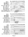
- FIG 6 illustrates an exemplary transfer of data at the request of a first processor from main memory to the processor's cache unit and can be contrasted with the exemplary transfer of modified data, at the request of a second processor, from the first processor's cache unit to the requesting processor's cache unit and to main memory.
- a processor e.g., processor JP0 ⁇
- the requesting processor supplies the address of the data requested, as well as the op-code information concerning its intended use of the data, onto the cache bus 37 (see signals MCU_A_DATA_0-30 and MCU_A_OPCODE_0-2).
- control unit 34 When it is determined that data resides in main memory and is valid data, the control unit 34 asserts the MCU_A_DATA_VALID signal and thereby controls the transfer of the data from main memory onto the main memory bus 38 and thence to the cache bus 37 for receipt and storage in cache unit 32.
- Processor JP0 ⁇ thereupon processes such data in a manner so as to modify the data.
- processor JP1 requests the modified data by asserting a request signal (MCU_REQUEST_HI_0)
- the control unit 34 again asserts a grant signal (MCU_A_GRANT_0) if the cache bus 37 is available.
- the modified data is identified by its address and op-code (MCU_A_DATA_0_31 and MCU_A_OPCOPE_0-2) which is placed on the cache bus 37.
- the control unit 34 asserts a signal (MCU_A_RESOLVE_ADDR) requesting that address coherency be checked before the modified data is permitted to be transferred.
- the MCU_A_RETURNING_BLOCK signal is asserted while a coherency check is being performed.
- the address supplied by the requesting processor is compared with the address of the modified data in the cache unit of the requested processor to assure that the data requested is identified correctly as the same data which has been so modified. If a comparison shows such a correct identification, then the valid modified data is placed on the cache bus 37 and on the main memory bus 38 (see MCU_A_DATA_VALID signal) for simultaneous transfer to the cache unit 33 of the requesting processor and to the main memory 35.
- a processor may access data and modify it for its own use but no other processor may request such modified data.
- the modified data is placed in the processors cache unit and remains there until it is requested by another processor in which case the modified data can be accessed from the first processor's cache unit and transferred simultaneously from such cache unit to the requesting processor's cache unit and to main memory in the manner discussed above.
- a processor's cache unit contains modified data which must be displaced from the cache unit, i.e., in order to make room therein for other data, the modified data can at that time be overwritten, although such modified data is still contained in main memory. If such modified data has been further subsequently modified before such displacement occurs, the further modified data must be transferred to main memory.
- the use of the system of FIG. 5 permits immediate transfer of modified data to a requesting cache unit and to main memory simultaneously using the cache and main memory buses.
- the time over which a modified data transaction is performed is reduced in comparison with prior systems and the overall system can provide a much higher data through-put than such previously known systems.
- Fig. 5 is used in the context of a system as depicted in Figs. 1 or 3, for example, wherein when the cache units are ported to two or more cache buses which are controlled by two or more memory control units, if one of the control units is used to control a modified data transfer operation with respect to one set of cache and memory buses, the other control units are available for use in performing completely independent processing/data transfer operations with respect to one or more of the processor/cache unit pairs and one or more of the other sets of cache and memory buses.
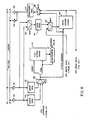
- FIG. 8 It is helpful in understanding the operation of a cache unit to consider a general block diagram of a typical cache unit as shown in FIG. 8. For simplicity, the unit is illustrated in the context of a system using two processors and two associated cache units (as in FIG. 1). Accordingly, the system uses two cache buses MCUB0 ⁇ and MCUB1 for transferring addresses and data. Different addresses which can be broadcast simultaneously, for example, on separate buses are supplied via incoming driver units 40 and 41 to address registers 42 and 43. The coherencies of such addresses must be determined to identify which address is intended for the cache unit in question.
- a tag store random access memory (RAM) 44 stores index and tag portions of all addresses in the associated cache data store RAM 45.
- RAM tag store random access memory
- the index and tag bits of each received address from registers 42 and 43 are examined in sequence, being supplied in such fashion via multiplexer (MUX) 46 to tag store 44, the tag bits being supplied to comparator logic 47.
- the tag bits are compared with the tag bits in tag store 44, which correspond to the addresses of data store 45, to determine if the received address corresponds to an address in data store 45. If such a correspondence exists, the comparator identifies the address as a valid data store address (ADDRESS VALID) i.e., the cache unit recognizes that a received address is intended for it. If no such correspondence is found, the cache unit identifies an incoming address as invalid for it and ignores it.
- ADRESS VALID a valid data store address
- the address is supplied to the data store RAM from MUX 46 and the address and data are subsequently supplied to an output register 47 in MUX 48 and thence to the same MCUB bus on which the address was originally received via outgoing bus driver units 49 and 50. If data is to be written into data store 44 at such valid address, the data is supplied to a data register 51 via MUX 52 and then to data store 45 via MUX 53.
- the processor associated with the cache unit is also provided with direct access to tag store 44 and data store 45 for providing addresses, and write and read data transfers, to and from the data store, as requested by the CPU, using MUX 46 and MUX 53, as shown.
- Appropriate operation of the units depicted in FIG. 8 can be controlled using suitable control logic (not shown) therefor in the cache unit, the design of appropriate control logic being well within the skill of those in the art.
- Such bus protocol provides for all data block transactions to and from main memory and also provides for inter-processor message passing and fox arbitrating access rights to memory blocks for preserving cache coherency.
- Each MCU bus has, for example, a 32 bit data path used for transmitting both addresses and data. Four byte-parity bits are associated with the data path. Double word addresses are right-justified on this data path, allowing a maximum address range to a specific system, for example, of 16 Gbytes.
- Arbitration of the MCU buses is performed centrally by the memory control units.
- Each requestor has its own bus interface circuitry and request lines, which are held high until the requestor has been granted an MCU bus.
- the granted requestor then presents this request by driving a 3-bit request opcode and an address on to the 32-bit data path.
- the opcodes and addresses also provide information to the other inteface circuits on the bus for performing cache coherency operations.
- MCU bus operations are transactionalized, that is, each interface circuit must preserve all information pertaining to its request until the successful completion of a bus transaction. If an error is detected during an operation transaction, the transaction will be subsequently retried, starting with the re-presentation of the opcode and address.
- Each MCU bus is controlled by its own memory control unit.
- all interface circuits are connected to both MCU buses and must participate in cache memory coherency operations on both such buses. Requests for service are made over separate request lines common to both buses and the memory control units associated therewith determine which bus will be granted to the requestor.
- Such systems may be operated as fault-tolerant systems, i.e., with the two memory control units and two MCU buses being redundant and running in lockstep.
- requestor pairs will be granted different buses, and each requestor will be inhibited from performing cache coherency operations on the bus not serving it.
- the following eight op-code operations are defined for the MCU buses, as 000 No Operation (NOP) 001 Read with Read-Only Access (Read_RO) 010 Swap with Read-Only Access (Swap_RO) 011 Send Message (Send) 100 Upgrade Access to Read-Write (Upgrade) 101 Read with Read-Write Access (Read_RW) 110 Swap with Read-Write Access (Swap_RW) 111 Write Block (write)
- caches interface circuits may have to perform one or more of the following sub-operations in order to complete an operation: - Cache Coherency Check - Invalidate Block - Transfer Block - NACK (Block Locked) - Receive Message - NACK (Cannot Take Message)
- NOP opcode is driven onto the opcode lines, and no further actions occur. No cache coherency checks occur, and the memory control unit is free to grant the bus to another requestor at the first available opportunity.
- the requestor drives the opcode lines with the appropriate Read opcode, and the address of the block desired, specifying which double word is desired first.
- the block is transferred to the requestor by the memory control unit or by another cache which may be holding the block.
- Swap operations of either a Read-Only Access type or Read-Write Access type the Swap involves both the reading of a block and the writing back of a block to update main memory.
- a Swap Operation is used only when a cache must displace modified data therein.
- the requestor drives the opcode lines with the Send opcode, and the address lines to specify the message destination or destinations.
- the data lines are subsequently driven with the four double word message.
- the destination returns a NACK if the message cannot be taken at that time.
- An Upgrade operation is one intended to modify a block in a cache and, for that purpose, the cache must upgrade its ability to write.
- the requestor drives the opcode lines with the Upgrade opcode, and the address lines with the address of the block that Read-Write access is desired for. All other caches perform a cache consistency check with the address, and take appropriate cache consistency actions.
- the Upgrade is granted if no inconsistent conditions are found within a given number of cycles. For example, if a NACK is asserted by another cache (indicating that the other cache is modifying the same data) an Upgrade is not granted.
- a Write Block is essentially exclusively used for I/O operations.
- an I/O controller desires to transfer data from an I/O device to main memory. If the data is modified by the I/O device, then the other caches must validate that data block if it is contained therein. Each cache makes a cache coherency check to see if it has the block and, if it does, the cache validates that data block.
- cache coherency checking For Cache Coherency and Block Locking sub-operations, the purpose of cache coherency checking is to insure that all copies of a cache block in the system are identical. In order to maintain this consistency, shared access to cache blocks may have to be restricted under certain circumstances.
- a Cache Interface which holds a cache block does so in one of four access modes, namely, Read-Only, Read-Write, Lock, or Write-Only modes.
- Read-Only access is the only access mode in which simultaneous sharing of a block among caches is permitted. Since the block cannot be modified by any cache which is holding it, all copies are valid. All caches holding a shared block must hold it with Read-Only access while it is being shared, and all must invalidate their copy of the block if it is requested in another access mode.
- Read-Write access is an exclusive access mode, i.e., no other cache may hold a particular block, in any access mode, while one cache holds it in a Read-Write access mode. If another requestor request a block being held with Read-Write access, the cache holding the block must transfer the block to that requestor. Read access to the block may be retained if the request is for a Read-Only access mode.
- Locked access is an uninterruptible Read-Write access mode. To prevent deadlock, each cache may only hold a lock on one block at a time. A cache must hold a block with Read-Write access before it locks it, to insure exclusivity and may only hold a lock on a block for one instruction before releasing the lock. If another requestor requests a block while it is locked, the cache holding the block returns a NACK to the requestor. The requestor should then re-request the block at a later time.
- each request on an MCU bus must be evaluated by every cache in the system to determine whether any actions need to be taken to preserve cache coherency.
- Cache coherency must be checked for the operations of Reads, Writes, Swaps, and Upgrades. No cache coherency checks should be performed for message transmissions, as they do not involve cache blocks.
- Certain actions may have to be performed by caches holding blocks requested by others, in order to preserve cache coherency. Such actions include invalidating a block, downgrading access to a block from Read-Write to Read-Only, transferring a block to a requestor, and sending a NACK to a requestor.
- a cache "holding" a block with Write-Only access need not resolve cache coherency with respect to the block to be written and the cache merely writes the block when it is granted the bus.
- An MCU bus further provides a message passing mechanism as a means of interprocessor communications.
- the higher levels of message protocol i.e., the meanings of the fields in a message, are not defined by the MCU bus protocol. Messages are defined as four double words long. They can be sent to one or several processors simultaneously.
- a cache interface to the MCU buses should have the ability to buffer at least one message. If a message is sent to a cache interface when that interface's buffer is full, the interface must assert the NACK signal to indicate this condition. In this case, the sending interface should wait several cycles, then repeat the attempt to send the message.
- message destination addresses are transmitted in a decoded manner.
- More than one line in the address is asserted.
- Processor addresses for example, are determined by the position they occupy on a chassis of the system.
- a requestor may make its request at an appropriate priority level, e.g., a HI priority level.
- the requestor asserts its MCU_REQUEST_HI line and must continue to assert this line until an MCU asserts either an MCU_A_GRANT or an MCU_B_GRANT. If an MCU_A_GRANT is asserted, the operation will take place over MCU bus A, and if MCU_B_GRANT is asserted, the operation will take place over MCU bus B.
- the requestor In the cycle following the MCU's assertion of a GRANT signal, the requestor must drop its REQUEST signal and drive the MCU_OPCODE, MCU_DATA, and MCU_PAR lines on the granted bus with the opcode and address of its desired operation.
- the MCU_RESOLVE_ADDR line of that bus must be asserted if the operation requires a Cache Coherency Check. These lines must only be driven for one cycle.
- the dropping of the MCU_OPCODE, MCU_DATA ⁇ and MCU_PAR signals at the end of the cycle in which they were driven completes the Arbitration and Grant Phase. The operation then continues with the operation-specific protocol.
- an MCU_BUS_ERROR signal for the affected bus is asserted by the unit detecting the error, and the requestor must re-initiate the Read Operation, beginning with requesting the bus. The requestor must keep track of the number of re-attempts, and the attempts can be abandoned at some selected point.
- the requestor waits the assertion of the MCU_XMIT_NEXT_CYCLE line on the granted bus. In the four cycles immediately following the assertion of this signal, the requestor drives the four double words to be written onto the MCU_DATA and MCU_PAR lines of the granted bus.
- a Write Operation is completed either by the assertion of the MCU-COMPLETE signal by the MCU, or by the assertion of an MCU_BUS_ERROR signal. If an MCU_BUS_ERROR signal is asserted, the requestor must re-initiate the entire Write operation, beginning with requesting the bus.
- a Swap operation is essentially a Read Operation followed by a Write Operation.
- One exception to this is that only the Read address is checked for Cache Coherency.
- the requestor drives the address for the Read Operation portion of the Swap operation. Following the Arbitration and Grant Phase, the requestor awaits a second assertion of the MCU-GRANT signal for the granted bus. On the cycle following the second assertion, the requestor drives the MCU_DATA and MCU_PAR lines of the granted bus with the address for the Write Operation. These lines are driven for one cycle only.
- the requestor awaits the assertion of the MCU_DATA_VALID signal to indicate that the first double word of the Read data is valid on the bus. Transfer of the Read data continues in the next three cycles following the assertion of MCU_DATA_VALID.
- the requestor next awaits the assertion of MCU_XMIT_NEXT_CYCLE. This assertion may occur during the last cycle of the Read data transfer. On the four cycles following the assertion of MCU_XMIT_NEXT_CYCLE, the requestor drives the four double words to be written.
- the Swap Operation is completed either by the assertion of the MCU-COMPLETE signal, or by the assertion of an MCU_BUS_ERROR signal.
- the requesting cache must continue to perform Cache Coherency Checks on the block to be written until the assertion of the MCU-COMPLETE signal. If an MCU_BUS_ERROR signal is asserted, the requesting cache must re-initiate the entire Swap operation, beginning with requesting the bus.
- the requestor For an Upgrade Access Operation, discussed with reference to FIG. 13, following the Arbitration and Grant Phase, the requestor must wait a selected number of cycles, e.g., four cycles. If the MCU_REQUEST_NACK signal is asserted on the granted bus during the fourth cycle following the driving of the bus, the block is locked, and the requestor must re-initiate the Upgrade Operation later. If no NACK is asserted, the Upgrade is considered to be granted.
- the requestor For a Send Message Operation, discussed with reference to FIG. 14, following the Arbitration and Grant Phase, the requestor must wait a selected number of cycles, e.g., four cycles. At the end of the fourth cycle the intended message recipient must be driving either the signal CLR_TO_SEND_MSG or REQUEST_NACK on the involved bus. A CLR_TO_SEND_MSG indicates that the message can be accepted, and a REQUEST_NACK indicates that the message cannot be taken at this time. At any time following the fourth cycle, the MCU will assert the signal XMIT_NEXT_CYCLE. On the cycle following XMIT_NEXT_CYCLE, the requestor must transmit the first double word of the message, the assert DATA_VALID. On the following three cycles, the remaining three double words of the message are transmitted, and DATA_VALID is dropped.
- a selected number of cycles e.g., four cycles.
- the intended message recipient At the end of the fourth cycle the intended message recipient must be driving either the
- a REQUEST_NACK signal is the response of the recipient to the message request, the request must be retried at a later time. If an MCU_BUS_ERROR signal is asserted, the requestor must re-initiate the operation, beginning with requesting the bus.
- a Cache Coherency Check begins with the Arbitration and Grant Phase of an operation.
- the RESOLVE_ADDR signal for the MCU bus that is involved will be asserted if the address must be checked.
- each interface must insure that the address and opcode have been registered from the bus.
- the invalidation must be carried out immediately (within a cycle, for example, of the RESOLVE_ADDR). No MCU bus signal needs to be asserted to indicate that an invalidation has taken place.
- a RETURNING_BLOCK signal must be asserted on the bus that is involved as soon as the need to transfer is determined. At the latest, the signal must be asserted by a selected cycle, e.g., the third cycle, following the RESOLVE_ADDR. A RETURNING_BLOCK signal must be held asserted until the subsequent Transfer Block Sub-Operation is complete.
- the REQUEST_NACK signal on the involved bus must be asserted as soon as possible following the determination of the need to NACK.. At the latest, it must be raised during a selected cycle, e.g., the third cycle following the RESOLVE_ADDR. REQUEST_NACK must be held through the fourth cycle following the RESOLVE_NACK and then dropped.
- the RETURNING_BLOCK signal must be raised as specified in the Cache Coherency Check sub-operation.
- the RETURNING_BLOCK signal is held while the block is fetched from the cache and transferred.
- the transferring cache may not begin to transfer the block before the sixth cycle, for example, following RESOLVE_ADDR.
- the block must be transferred with the desired double word transferred first.
- the transferring cache drives the first double word of the block onto the bus, and asserts the DATA_VALID signal for one cycle.
- the remaining three double words of the block are driven onto the bus, and the DATA_VALID signal is dropped.
- the RETURNING_BLOCK signal is dropped in the cycle following the driving of the second double word.
- messages are address in a decoded manner, with each line of DATA_0-31 corresponding to a processor.
- the Send Message opcode (011) is driven onto the OPCODE lines of an MCU bus, the line on that MCU bus corresponding to the processor should be checked to see if a request is being made to send a message to that, processor.
- the processor When a message request has been made to a processor, the processor must assert the CLR_TO_SEND_MSG signal on that bus if it can receive the message, or assert the REQUEST_NACK signal on that bus if it cannot receive a message at that time. Either signal should be raised by the third cycle following the Send Message request, and must be held through the fourth cycle following the request.
- the receiving processor awaits the DATA_VALID signal on the involved bus.
- the message is transmitted during the cycle that DATA_VALID is asserted and the three following cycles message requests should be NACKed when the incoming message buffer is full, or when other bus operations in progress make it impossible to control a message reception.
- the interface detecting the error should assert and hold the BUS_ERROR line on the involved bus.
- the signal should be held through the end of any pending operation on that bus. Any operation in progress when the BUS_ERROR signal is asserted must be restarted form the beginning, and the bus must be re-requested.
Landscapes
- Engineering & Computer Science (AREA)
- Theoretical Computer Science (AREA)
- Physics & Mathematics (AREA)
- General Engineering & Computer Science (AREA)
- General Physics & Mathematics (AREA)
- Memory System Of A Hierarchy Structure (AREA)
Applications Claiming Priority (2)
| Application Number | Priority Date | Filing Date | Title |
|---|---|---|---|
| US25036488A | 1988-09-28 | 1988-09-28 | |
| US250364 | 1988-09-28 |
Publications (2)
| Publication Number | Publication Date |
|---|---|
| EP0361887A2 true EP0361887A2 (de) | 1990-04-04 |
| EP0361887A3 EP0361887A3 (de) | 1991-07-24 |
Family
ID=22947422
Family Applications (1)
| Application Number | Title | Priority Date | Filing Date |
|---|---|---|---|
| EP19890309827 Withdrawn EP0361887A3 (de) | 1988-09-28 | 1989-09-27 | Multiprozessor/Cache-Speicheranordnung und Datenvorgangssteuerung dafür |
Country Status (3)
| Country | Link |
|---|---|
| EP (1) | EP0361887A3 (de) |
| JP (1) | JPH02186455A (de) |
| AU (1) | AU617514B2 (de) |
Cited By (1)
| Publication number | Priority date | Publication date | Assignee | Title |
|---|---|---|---|---|
| CN114820271A (zh) * | 2021-01-28 | 2022-07-29 | Arm有限公司 | 数据处理系统 |
Families Citing this family (1)
| Publication number | Priority date | Publication date | Assignee | Title |
|---|---|---|---|---|
| DE4135553A1 (de) * | 1991-10-29 | 1993-05-06 | Alcatel Sel Aktiengesellschaft, 7000 Stuttgart, De | Verfahren und schaltungsanordnung zur datenblockuebertragung ueber ein bussystem |
-
1989
- 1989-08-25 AU AU40268/89A patent/AU617514B2/en not_active Ceased
- 1989-09-27 EP EP19890309827 patent/EP0361887A3/de not_active Withdrawn
- 1989-09-27 JP JP1251697A patent/JPH02186455A/ja active Pending
Non-Patent Citations (2)
| Title |
|---|
| PROCEEDINGS OF THE 1988 INTERNATIONAL CONFERENCE ON PARALLEL PROCESSING, University Park, PA, 15th - 19th August 1988, vol. I: Architecture, pages 130-137; Q. YANG et al.: "A queueing network model for a cache coherence protocol on multiple-bus multiprocessors" * |
| PROCEEDINGS OF THE NATIONAL COMPUTER CONFERENCE, New York 7th - 10th June 1976, vol. 45, pages 749-753, AFIPS, Montvale, US; C.K. TANG: "Cache system design in the tightly coupled multiprocessor system" * |
Cited By (2)
| Publication number | Priority date | Publication date | Assignee | Title |
|---|---|---|---|---|
| CN114820271A (zh) * | 2021-01-28 | 2022-07-29 | Arm有限公司 | 数据处理系统 |
| CN114820271B (zh) * | 2021-01-28 | 2026-06-16 | Arm有限公司 | 数据处理系统 |
Also Published As
| Publication number | Publication date |
|---|---|
| AU617514B2 (en) | 1991-11-28 |
| JPH02186455A (ja) | 1990-07-20 |
| EP0361887A3 (de) | 1991-07-24 |
| AU4026889A (en) | 1990-04-05 |
Similar Documents
| Publication | Publication Date | Title |
|---|---|---|
| EP0777184B1 (de) | Cachespeicherkohärenzverfahren und-system | |
| US5263142A (en) | Input/output cache with mapped pages allocated for caching direct (virtual) memory access input/output data based on type of I/O devices | |
| US4843542A (en) | Virtual memory cache for use in multi-processing systems | |
| US6353877B1 (en) | Performance optimization and system bus duty cycle reduction by I/O bridge partial cache line write | |
| US6012120A (en) | Method and apparatus for providing DMA transfers between devices coupled to different host bus bridges | |
| EP0283628B1 (de) | Busschnittstellenschaltung für digitalen Datenprozessor | |
| US6021456A (en) | Method for communicating interrupt data structure in a multi-processor computer system | |
| EP0303661B1 (de) | Zentraleinheit für digitales datenverarbeitungssystem, mit schreibpufferverwaltungsmechnismus | |
| EP0288649B1 (de) | Speichersteuersystem | |
| US6587931B1 (en) | Directory-based cache coherency system supporting multiple instruction processor and input/output caches | |
| US5113514A (en) | System bus for multiprocessor computer system | |
| EP0524683A1 (de) | Wissenschaftliches Anzeigesystem | |
| EP0303648B1 (de) | Zentralprozessoreinheit für digitale datenverarbeitungsanordnung mit cache-speicherverwaltungsvorrichtung | |
| US5091845A (en) | System for controlling the storage of information in a cache memory | |
| JPH08249231A (ja) | マルチプロセッサ・システムにおける古いデータの処理システム及び方法 | |
| EP0480858A2 (de) | Hardware-Verriegelung für primäres Verzeichnis | |
| JPH05274252A (ja) | コンピュータシステムにおけるトランザクション実行方法 | |
| JPH07152647A (ja) | 共有メモリマルチプロセッサ | |
| US5923857A (en) | Method and apparatus for ordering writeback data transfers on a bus | |
| AU606083B2 (en) | Interface between processor and special instruction processor in digital data processing system | |
| AU617514B2 (en) | Multiple processor/cache memory system and data transaction control therefor | |
| US5488706A (en) | Retry request system in a pipeline data processing system where each requesting unit preserves the order of requests | |
| US5809534A (en) | Performing a write cycle to memory in a multi-processor system | |
| US8108618B2 (en) | Method and apparatus for maintaining memory data integrity in an information handling system using cache coherency protocols | |
| CA2036372C (en) | An input/output cache for caching direct (virtual) memory access data |
Legal Events
| Date | Code | Title | Description |
|---|---|---|---|
| PUAI | Public reference made under article 153(3) epc to a published international application that has entered the european phase |
Free format text: ORIGINAL CODE: 0009012 |
|
| AK | Designated contracting states |
Kind code of ref document: A2 Designated state(s): DE FR GB |
|
| PUAL | Search report despatched |
Free format text: ORIGINAL CODE: 0009013 |
|
| AK | Designated contracting states |
Kind code of ref document: A3 Designated state(s): DE FR GB |
|
| STAA | Information on the status of an ep patent application or granted ep patent |
Free format text: STATUS: THE APPLICATION IS DEEMED TO BE WITHDRAWN |
|
| 18D | Application deemed to be withdrawn |
Effective date: 19920125 |