EP0363422B1 - Tete integree de lecture/ecriture optique et appareil pourvu de cette tete - Google Patents
Tete integree de lecture/ecriture optique et appareil pourvu de cette tete Download PDFInfo
- Publication number
- EP0363422B1 EP0363422B1 EP88905541A EP88905541A EP0363422B1 EP 0363422 B1 EP0363422 B1 EP 0363422B1 EP 88905541 A EP88905541 A EP 88905541A EP 88905541 A EP88905541 A EP 88905541A EP 0363422 B1 EP0363422 B1 EP 0363422B1
- Authority
- EP
- European Patent Office
- Prior art keywords
- waveguide
- electro
- substrate
- spot
- electrodes
- Prior art date
- Legal status (The legal status is an assumption and is not a legal conclusion. Google has not performed a legal analysis and makes no representation as to the accuracy of the status listed.)
- Expired - Lifetime
Links
- 230000003287 optical effect Effects 0.000 title claims abstract description 38
- 238000006073 displacement reaction Methods 0.000 claims abstract description 10
- 230000005855 radiation Effects 0.000 claims abstract description 9
- 230000005684 electric field Effects 0.000 claims abstract description 6
- 239000000758 substrate Substances 0.000 claims description 21
- 239000004973 liquid crystal related substance Substances 0.000 claims description 11
- VYPSYNLAJGMNEJ-UHFFFAOYSA-N Silicium dioxide Chemical compound O=[Si]=O VYPSYNLAJGMNEJ-UHFFFAOYSA-N 0.000 claims description 10
- 239000000382 optic material Substances 0.000 claims description 7
- 235000012239 silicon dioxide Nutrition 0.000 claims description 5
- 239000000377 silicon dioxide Substances 0.000 claims description 5
- 229910052710 silicon Inorganic materials 0.000 claims description 4
- 239000010703 silicon Substances 0.000 claims description 4
- 229910003327 LiNbO3 Inorganic materials 0.000 claims description 3
- 230000008859 change Effects 0.000 description 6
- 239000000463 material Substances 0.000 description 4
- XUIMIQQOPSSXEZ-UHFFFAOYSA-N Silicon Chemical compound [Si] XUIMIQQOPSSXEZ-UHFFFAOYSA-N 0.000 description 3
- 229910052681 coesite Inorganic materials 0.000 description 3
- 238000010276 construction Methods 0.000 description 3
- 229910052906 cristobalite Inorganic materials 0.000 description 3
- 239000010408 film Substances 0.000 description 3
- 229910052751 metal Inorganic materials 0.000 description 3
- 239000002184 metal Substances 0.000 description 3
- 238000000034 method Methods 0.000 description 3
- 229910052682 stishovite Inorganic materials 0.000 description 3
- 229910052905 tridymite Inorganic materials 0.000 description 3
- 230000000694 effects Effects 0.000 description 2
- 238000005516 engineering process Methods 0.000 description 2
- 239000011521 glass Substances 0.000 description 2
- AMGQUBHHOARCQH-UHFFFAOYSA-N indium;oxotin Chemical compound [In].[Sn]=O AMGQUBHHOARCQH-UHFFFAOYSA-N 0.000 description 2
- 239000010409 thin film Substances 0.000 description 2
- 235000010627 Phaseolus vulgaris Nutrition 0.000 description 1
- 244000046052 Phaseolus vulgaris Species 0.000 description 1
- 230000008878 coupling Effects 0.000 description 1
- 238000010168 coupling process Methods 0.000 description 1
- 238000005859 coupling reaction Methods 0.000 description 1
- HFGPZNIAWCZYJU-UHFFFAOYSA-N lead zirconate titanate Chemical compound [O-2].[O-2].[O-2].[O-2].[O-2].[Ti+4].[Zr+4].[Pb+2] HFGPZNIAWCZYJU-UHFFFAOYSA-N 0.000 description 1
- 229910052451 lead zirconate titanate Inorganic materials 0.000 description 1
- 230000000670 limiting effect Effects 0.000 description 1
- GQYHUHYESMUTHG-UHFFFAOYSA-N lithium niobate Chemical compound [Li+].[O-][Nb](=O)=O GQYHUHYESMUTHG-UHFFFAOYSA-N 0.000 description 1
- 238000004519 manufacturing process Methods 0.000 description 1
- 230000007246 mechanism Effects 0.000 description 1
- 238000001259 photo etching Methods 0.000 description 1
- 230000008569 process Effects 0.000 description 1
- 230000001902 propagating effect Effects 0.000 description 1
- 238000007493 shaping process Methods 0.000 description 1
- 239000004094 surface-active agent Substances 0.000 description 1
Images

Classifications
-
- G—PHYSICS
- G02—OPTICS
- G02F—OPTICAL DEVICES OR ARRANGEMENTS FOR THE CONTROL OF LIGHT BY MODIFICATION OF THE OPTICAL PROPERTIES OF THE MEDIA OF THE ELEMENTS INVOLVED THEREIN; NON-LINEAR OPTICS; FREQUENCY-CHANGING OF LIGHT; OPTICAL LOGIC ELEMENTS; OPTICAL ANALOGUE/DIGITAL CONVERTERS
- G02F1/00—Devices or arrangements for the control of the intensity, colour, phase, polarisation or direction of light arriving from an independent light source, e.g. switching, gating or modulating; Non-linear optics
- G02F1/29—Devices or arrangements for the control of the intensity, colour, phase, polarisation or direction of light arriving from an independent light source, e.g. switching, gating or modulating; Non-linear optics for the control of the position or the direction of light beams, i.e. deflection
- G02F1/295—Analog deflection from or in an optical waveguide structure]
- G02F1/2955—Analog deflection from or in an optical waveguide structure] by controlled diffraction or phased-array beam steering
-
- G—PHYSICS
- G11—INFORMATION STORAGE
- G11B—INFORMATION STORAGE BASED ON RELATIVE MOVEMENT BETWEEN RECORD CARRIER AND TRANSDUCER
- G11B7/00—Recording or reproducing by optical means, e.g. recording using a thermal beam of optical radiation by modifying optical properties or the physical structure, reproducing using an optical beam at lower power by sensing optical properties; Record carriers therefor
- G11B7/08—Disposition or mounting of heads or light sources relatively to record carriers
- G11B7/09—Disposition or mounting of heads or light sources relatively to record carriers with provision for moving the light beam or focus plane for the purpose of maintaining alignment of the light beam relative to the record carrier during transducing operation, e.g. to compensate for surface irregularities of the latter or for track following
-
- G—PHYSICS
- G11—INFORMATION STORAGE
- G11B—INFORMATION STORAGE BASED ON RELATIVE MOVEMENT BETWEEN RECORD CARRIER AND TRANSDUCER
- G11B7/00—Recording or reproducing by optical means, e.g. recording using a thermal beam of optical radiation by modifying optical properties or the physical structure, reproducing using an optical beam at lower power by sensing optical properties; Record carriers therefor
- G11B7/12—Heads, e.g. forming of the optical beam spot or modulation of the optical beam
- G11B7/123—Integrated head arrangements, e.g. with source and detectors mounted on the same substrate
- G11B7/124—Integrated head arrangements, e.g. with source and detectors mounted on the same substrate the integrated head arrangements including waveguides
- G11B7/1245—Integrated head arrangements, e.g. with source and detectors mounted on the same substrate the integrated head arrangements including waveguides the waveguides including means for electro-optical or acousto-optical deflection
Definitions
- This invention relates to the field of optical recording and, more particularly, to improvements in optical heads for writing and/or reading information on a radiation-sensitive recording element, such as an optical disk. More specifically, this invention relates to improvements in optical read/write heads of the type which employ integrated optics.
- optical systems typically comprise at least one diode laser, various bulk optical elements (e.g. prisms, lenses, mirrors, etc.) for expanding, shaping, deflecting and focusing the beam emitted by such laser, and a plurality of individual detectors which serve to detect from the laser energy reflected (or transmitted) by a recording element the recorded information.
- detectors also serve to develop focus and tracking errors signals for controlling the focus and tracking position of the laser beam on the recording element.
- miniaturized optical heads of the above type are sufficiently massive as to require significant time to settle into a read/write position after a "track jump" in which the head is rapidly moved relative to the recording element to access information at a different location.
- Such integrated optical heads also include a detector package for sensing light reflected obliquely from the recording element so as to detect the recorded information and the focus and tracking accuracy of the incident light. The respective outputs of such detectors are used to develop focus and tracking error signals which, in turn, are used to maintain the spot in precise focus on the recording element and to control the position of the spot relative to a desired track of information.
- the waveguide is made of a material (e.g. LiNbO3 or PLZT) which exhibits the well known electrooptic effect, and the focus and tracking error signals are used to selectively vary the refractive index of a portion of the waveguide which defines a control lens used to control the focus and tracking position of the read/write spot.
- a material e.g. LiNbO3 or PLZT
- Such variation is achieved by a complex array of closely spaced electrodes arranged on the top surface of the waveguide. When coupled to a voltage source, these electrodes produce fringing fields which alter the refractive index and shape of the integrated lens, thereby changing its focal length and causing the focused spot to move in a direction perpendicular to the optical axis.
- an apparatus for writing and/or reading information on a recording element having a plurality of data tracks along which such information is, or is to be, recorded comprising:
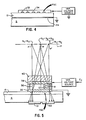
- FIGS. 1 and 2 schematically illustrate an integrated optical write/read head 10 structured in accordance with a preferred embodiment.
- Head 10 is shown in an operative position with respect to a moving optical recording element R (e.g. a conventional optical disk) which is provided with a plurality of spaced, parallel data tracks T along which data is to be written or read.
- R e.g. a conventional optical disk
- the head is maintained relatively stationary, and the recording element is moved in the direction of the arrow a, whereby a focused spot P of radiation produced by the head is scanned along a desired data track.
- Integrated optical head 10 may comprise a rigid, transparent substrate S, such as glass, which supports a planar optical waveguide 12.
- the substrate may be a silicon wafer having a thermallly grown, transparent buffer layer of SiO2. It will be appreciated that the drawing is not to scale since the substrate thickness is typically of the the order of a millimeter, whereas the waveguide thickness is usually less than one micron.
- Laser energy emanating from a diode laser L or the like is coupled into the waveguide in a conventional manner, such as by "butt coupling" the diode laser output to the waveguide edge, as shown.
- Laser energy E diverging from diode laser and propagating through the waveguide is collimated by an integrated lens 14 to form a collimated beam B having an axis A.
- Lens 14 may take the form of any of the lenses (Luneburg, Fresnel, Bragg, etc.) mentioned above.
- a conventional focusing grating coupler (FGC) also integrated in the waveguide, is positioned to intercept beam B and to couple such beam out of the waveguide at an egress zone Z to form the focused spot P on the recording element.
- FGC focusing grating coupler
- the focused beam Upon striking the recording element, the focused beam is reflected back toward the waveguide, and a part of the reflected energy passes through the waveguide and its supporting substrate, (or through the SiO2 buffer layer in the case of an SiO2 overcoated silicon substrate) and-is incident on a pair of spaced detectors D1, D2, arranged on the bottom surface of the substrate, (or the top of the substrate, in the case of a silicon substrate).
- the respective outputs of the detectors D1 and D2 are subtracted by a differential amplifier, A1, to provide a tracking error signal E T which is used to control the tracking position of the focused spot P, in the manner described below.
- the respective outputs of detectors D1 and D2 can be summed, via summing amplifier A2, to provide a signal RF representing the recorded data.
- means are provided, in accordance with this invention, for selectively varying the "effective" refractive index, n eff of that portion of the waveguide in the region of the focus grating coupler (i.e. zone Z) by an amount proportional to the tracking error signal E T .
- n eff refractive index
- zone Z region Z
- E T tracking error signal
- this principle is used to precisely maintain the position of the focused spot P on a desired data track.
- Variations in the effective refractive index of the waveguide can be achieved by varying the refractive index of the waveguide itself, or, alternatively, by varying the refractive index of an adjacent or closely proximate layer, such as substrate S or a transparent covering layer, described with reference to FIG. 5 below.
- the waveguide comprises an electro-optic material (e.g. lanthanium-doped lead zirconate titanate (PLZT) or lithium niobate (LiNbO3)) whose refractive index is variable, depending upon the strength of an applied electric field.
- electro-optic material e.g. lanthanium-doped lead zirconate titanate (PLZT) or lithium niobate (LiNbO3)
- Such refractive index varying-means comprises a pair of transparent, plane, parallel electrodes 22, 24 positioned on opposite sides of the waveguide, in the vicinity of the focused grating coupler, and a variable voltage source 20 for producing a variable electric field across that portion of the waveguide between the electrodes, the strength of such field being determined by the tracking error signal E T .
- Electrodes 22 and 24 may comprise, for example, transparent thin films of indium tin oxide, about 0.1 microns or less in thickness. Such films may be sputter or vapor deposited in a conventional manner. To facilitate the manufacturing process, electrode 24 may cover the entire substrate surface. Preferably, however, the electrode 24 should be restricted to the area beneath the FGC to minimize optical losses.
- Electrode 22 need only cover the focused grating coupler. Electrode 24 may be grounded and electrode 22 connected to the output V s of the variable voltage source 20, as shown.
- the output of the variable voltage source 20 is determined by its input, E T which, as mentioned above, is determined by the amount by which the focused spot P is displaced from a desired track.
- E T is determined by the input, E T which, as mentioned above, is determined by the amount by which the focused spot P is displaced from a desired track.
- V s varies about a nominal level
- the focused spot P can be positioned anywhere within the angular range ⁇ , from P′ to P′′.
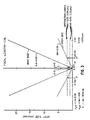
- n eff For sufficiently small changes in n eff about some nominal value, it has been observed that 1) a linear relationship exists between spot displacement (x) and n eff ; 2) the motion of the focus spot remains in a plane p (FIG. 2) parallel to the waveguide plane; and 3) the spot size remains diffraction limited over a displacement range (2x) determined by the effective numerical aperture (NA) of the focusing lens, in this case the FGC.
- NA effective numerical aperture
- 3 graph are the corresponding calculated diffraction-limited spot sizes (horizontal dashed lines) for the two values of NA for a wavelength of 830 nm. It will be noted that the spot sizes vary linearly with spot displacement x, and that the slopes of spot size-vs-x curves are proportional to the lens NA. From the graph, it is seen that the spot remains diffraction limited for ⁇ 5 microns for an NA of 0.45 and ⁇ 30 microns for an NA of 0.25. A deflection range of ⁇ 5 microns is sufficient to eliminate detracking mechanisms such as spindle-axis run-out and track out-of-roundness in conventional optical disk recording systems. These values of x correspond to changes ⁇ n eff of 0.0005 and 0.003, respectively.
- the focused grating coupler is formed by a patterned metal 33 formed atop the waveguide. Uniform electrical contact is assured by overcoating the metal with a transparent conductive film 34 (e.g ITO).
- a transparent conductive film 34 e.g ITO.
- Such patterned metal grating can be produced by conventional photo-etching techniques.
- an alternative technique for varying the effective refractive index of the waveguide and, hence, the angle at which the light is coupled out of the waveguide is to vary the refractive index of an adjacent or closely proximate layer.
- the theory of this approach is discussed in Journal of Lightwave Technology, Vol. LT-4, No. 3, March 1986, pp. 360-363.
- This indirect approach of changing the waveguide's effective refractive index offers several advantages over the previously described embodiment. For example, there is no need for the waveguide to comprise an electro-optic material; any passive optical waveguide material can be used as the waveguiding film 12. Further, the waveguide may be disposed directly on the substrate S, and there is no need for forming a planar transparent electrode between the substrate and waveguide.
- substrate S supports a waveguide 12 and its integrated focus grating lens (FGC) as in FIG. 1.
- FGC integrated focus grating lens
- a liquid crystal layer 30 is placed between two thin transparent electrode layers 36 and 38, for example, thin films of indium tin oxide (ITO).
- the lower ITO layer 36 is positioned atop the focus grating lens, and the upper electrode 34 is supported by a glass plate 40.
- the liquid crystal 30 may take the form of Merck's Type TCHll32 liquid crystal having an ordinary refractive index n o of about 1.50 and an extraordinary refractive index, n e , of about 1.63.
- Waveguide 12 is of a thickness of about 0.3 microns.
- the effective index of refraction (n eff ) of the single TE mode of the waveguide will depend on the index of refraction of the medium on both sides of the waveguide. Hence, n eff will depend on the state of the liquid crystal overlayer cell.
- the extraordinary axis E of a liquid crystal molecule will lie in the plane of the waveguide, perpendicular to the direction of light propagation, i.e., parallel to the direction established by a surfactant applied to the upper and lower electrode surfaces.
- an applied voltage intermediate these two extremes will result in an n eff between the two values.
- an applied voltage of 4 volts between electrodes 32 and 34 in the arrangement of FIG. 4 is sufficient to rotate the liquid crystal molecules from one orientation to the other.
- This change in refractive index of the liquid crystal layer will produce a total spot deflection of 500 microns for a lens having a focal length of 1 cm.
- variations of the intermediate bias voltage of much less than one volt would be required between electrodes 32 and 34.
- n c n e and the spot focus is at P′′.
- n c n o and the spot focus is at P′.
- n c (n e + n o )/2 and the spot focus is at P.
- the integrated read/write optical head of the invention is advantageous in that it is capable of maintaining track through the application of relatively low voltages, voltages applied across the thickness of the waveguide (or a proximate layer), and is of a much simpler construction vis-a-vis the aforementioned prior art devices.
Landscapes
- Physics & Mathematics (AREA)
- Optics & Photonics (AREA)
- Nonlinear Science (AREA)
- General Physics & Mathematics (AREA)
- Optical Head (AREA)
- Optical Recording Or Reproduction (AREA)
- Optical Integrated Circuits (AREA)
Abstract
Claims (8)
Applications Claiming Priority (2)
| Application Number | Priority Date | Filing Date | Title |
|---|---|---|---|
| US07/062,524 US4801184A (en) | 1987-06-15 | 1987-06-15 | Integrated optical read/write head and apparatus incorporating same |
| US62524 | 1998-04-17 |
Publications (2)
| Publication Number | Publication Date |
|---|---|
| EP0363422A1 EP0363422A1 (fr) | 1990-04-18 |
| EP0363422B1 true EP0363422B1 (fr) | 1991-10-23 |
Family
ID=22043047
Family Applications (1)
| Application Number | Title | Priority Date | Filing Date |
|---|---|---|---|
| EP88905541A Expired - Lifetime EP0363422B1 (fr) | 1987-06-15 | 1988-06-06 | Tete integree de lecture/ecriture optique et appareil pourvu de cette tete |
Country Status (5)
| Country | Link |
|---|---|
| US (1) | US4801184A (fr) |
| EP (1) | EP0363422B1 (fr) |
| JP (1) | JPH02501247A (fr) |
| DE (1) | DE3865841D1 (fr) |
| WO (1) | WO1988010493A1 (fr) |
Families Citing this family (47)
| Publication number | Priority date | Publication date | Assignee | Title |
|---|---|---|---|---|
| JP2539406B2 (ja) * | 1987-02-04 | 1996-10-02 | 株式会社日立製作所 | 固体光ピツクアツプ |
| JP2644829B2 (ja) * | 1988-06-24 | 1997-08-25 | 株式会社リコー | 光情報記録再生装置 |
| US5082339A (en) * | 1988-07-11 | 1992-01-21 | Telefunken Electronic Gmbh | Optical read-write head with diffraction grating structure |
| KR940004570B1 (ko) * | 1988-08-05 | 1994-05-25 | 마쓰시다 덴끼 산교오 가부시기가이샤 | 가변 초점 장치 |
| JP2749107B2 (ja) * | 1989-03-20 | 1998-05-13 | 株式会社日立製作所 | 光ヘッド |
| US4995689A (en) * | 1989-08-09 | 1991-02-26 | Eastman Kodak Company | Waveguide scanner |
| US5101458A (en) * | 1990-11-08 | 1992-03-31 | The University Of Rochester | Achromatic input/output coupler for integrated optical circuits |
| US5289454A (en) | 1991-12-19 | 1994-02-22 | Minnesota Mining And Manufacturing Company | Optical disc addressing devices a method of use thereof |
| US5238877A (en) * | 1992-04-30 | 1993-08-24 | The United States Of America As Represented By The Secretary Of The Navy | Conformal method of fabricating an optical waveguide on a semiconductor substrate |
| US5276745A (en) * | 1992-10-15 | 1994-01-04 | Eastman Kodak Company | Integrated optic read/write head for optical data storage incorporating second harmonic generator, electro-optic tracking error actuator, and electro-optic modulator |
| US5625725A (en) * | 1993-12-28 | 1997-04-29 | Sony Corporation | Magneto-optical pickup device having phase compensating circuitry |
| US6392257B1 (en) | 2000-02-10 | 2002-05-21 | Motorola Inc. | Semiconductor structure, semiconductor device, communicating device, integrated circuit, and process for fabricating the same |
| US6693033B2 (en) * | 2000-02-10 | 2004-02-17 | Motorola, Inc. | Method of removing an amorphous oxide from a monocrystalline surface |
| AU2001257346A1 (en) | 2000-05-31 | 2001-12-11 | Motorola, Inc. | Semiconductor device and method for manufacturing the same |
| WO2002009187A2 (fr) * | 2000-07-24 | 2002-01-31 | Motorola, Inc. | Diodes a heterojonction tunnel et processus de fabrication de celles-ci |
| US20020096683A1 (en) * | 2001-01-19 | 2002-07-25 | Motorola, Inc. | Structure and method for fabricating GaN devices utilizing the formation of a compliant substrate |
| WO2002082551A1 (fr) | 2001-04-02 | 2002-10-17 | Motorola, Inc. | Structure de semi-conducteur a courant de fuite attenue |
| US6709989B2 (en) | 2001-06-21 | 2004-03-23 | Motorola, Inc. | Method for fabricating a semiconductor structure including a metal oxide interface with silicon |
| US6992321B2 (en) | 2001-07-13 | 2006-01-31 | Motorola, Inc. | Structure and method for fabricating semiconductor structures and devices utilizing piezoelectric materials |
| US20030010992A1 (en) * | 2001-07-16 | 2003-01-16 | Motorola, Inc. | Semiconductor structure and method for implementing cross-point switch functionality |
| US7019332B2 (en) * | 2001-07-20 | 2006-03-28 | Freescale Semiconductor, Inc. | Fabrication of a wavelength locker within a semiconductor structure |
| US6693298B2 (en) | 2001-07-20 | 2004-02-17 | Motorola, Inc. | Structure and method for fabricating epitaxial semiconductor on insulator (SOI) structures and devices utilizing the formation of a compliant substrate for materials used to form same |
| US6855992B2 (en) * | 2001-07-24 | 2005-02-15 | Motorola Inc. | Structure and method for fabricating configurable transistor devices utilizing the formation of a compliant substrate for materials used to form the same |
| US20030026310A1 (en) * | 2001-08-06 | 2003-02-06 | Motorola, Inc. | Structure and method for fabrication for a lighting device |
| US6639249B2 (en) * | 2001-08-06 | 2003-10-28 | Motorola, Inc. | Structure and method for fabrication for a solid-state lighting device |
| US20030034491A1 (en) | 2001-08-14 | 2003-02-20 | Motorola, Inc. | Structure and method for fabricating semiconductor structures and devices for detecting an object |
| US6673667B2 (en) * | 2001-08-15 | 2004-01-06 | Motorola, Inc. | Method for manufacturing a substantially integral monolithic apparatus including a plurality of semiconductor materials |
| JP3963313B2 (ja) * | 2001-09-05 | 2007-08-22 | 日本碍子株式会社 | 光導波路デバイス、光変調器および光変調器の実装構造 |
| US20030071327A1 (en) | 2001-10-17 | 2003-04-17 | Motorola, Inc. | Method and apparatus utilizing monocrystalline insulator |
| AU2002351079A1 (en) * | 2001-11-29 | 2003-06-10 | Koninklijke Philips Electronics N.V. | Optical scanning device |
| US6916717B2 (en) * | 2002-05-03 | 2005-07-12 | Motorola, Inc. | Method for growing a monocrystalline oxide layer and for fabricating a semiconductor device on a monocrystalline substrate |
| US20040012037A1 (en) * | 2002-07-18 | 2004-01-22 | Motorola, Inc. | Hetero-integration of semiconductor materials on silicon |
| US20040070312A1 (en) * | 2002-10-10 | 2004-04-15 | Motorola, Inc. | Integrated circuit and process for fabricating the same |
| US20040069991A1 (en) * | 2002-10-10 | 2004-04-15 | Motorola, Inc. | Perovskite cuprate electronic device structure and process |
| US7169619B2 (en) * | 2002-11-19 | 2007-01-30 | Freescale Semiconductor, Inc. | Method for fabricating semiconductor structures on vicinal substrates using a low temperature, low pressure, alkaline earth metal-rich process |
| US6885065B2 (en) | 2002-11-20 | 2005-04-26 | Freescale Semiconductor, Inc. | Ferromagnetic semiconductor structure and method for forming the same |
| US6806202B2 (en) | 2002-12-03 | 2004-10-19 | Motorola, Inc. | Method of removing silicon oxide from a surface of a substrate |
| US6963090B2 (en) | 2003-01-09 | 2005-11-08 | Freescale Semiconductor, Inc. | Enhancement mode metal-oxide-semiconductor field effect transistor |
| US6965128B2 (en) * | 2003-02-03 | 2005-11-15 | Freescale Semiconductor, Inc. | Structure and method for fabricating semiconductor microresonator devices |
| US20040164315A1 (en) * | 2003-02-25 | 2004-08-26 | Motorola, Inc. | Structure and device including a tunneling piezoelectric switch and method of forming same |
| KR100584703B1 (ko) * | 2003-12-26 | 2006-05-30 | 한국전자통신연구원 | 평면 격자렌즈 |
| KR100835579B1 (ko) * | 2005-03-03 | 2008-06-09 | 스미도모쥬기가이고교 가부시키가이샤 | 광학부품의 수지성형방법, 금형장치, 및 게이트 부시 |
| TWI572912B (zh) * | 2012-12-17 | 2017-03-01 | 鴻海精密工業股份有限公司 | 光調變器 |
| CN105182463A (zh) * | 2015-08-14 | 2015-12-23 | 深圳市华星光电技术有限公司 | 一种导光板及显示装置 |
| US9864139B1 (en) * | 2016-01-22 | 2018-01-09 | Seagate Technology Llc | Uniform laser direct writing for waveguides |
| US10288808B1 (en) | 2016-01-22 | 2019-05-14 | Seagate Technology Llc | Laser direct writing for non-linear waveguides |
| CN113866881B (zh) * | 2021-09-18 | 2022-07-05 | 华中科技大学 | 一种模斑转换器 |
Family Cites Families (19)
| Publication number | Priority date | Publication date | Assignee | Title |
|---|---|---|---|---|
| US3871747A (en) * | 1972-10-03 | 1975-03-18 | Us Navy | Optical waveguide display panel |
| US3898585A (en) * | 1974-01-14 | 1975-08-05 | Ibm | Leaky corrugated optical waveguide device |
| DE2442723A1 (de) * | 1974-09-06 | 1976-03-18 | Siemens Ag | Steuerbarer elektrooptischer gitterkoppler |
| US3951513A (en) * | 1974-09-09 | 1976-04-20 | Masi James V | Semiconductor light modulating optical wave guide |
| US4047795A (en) * | 1974-11-22 | 1977-09-13 | The United States Of America As Represented By The Secretary Of The Navy | Optical integrated circuit laser beam scanner |
| DE2543469A1 (de) * | 1975-09-29 | 1977-06-02 | Siemens Ag | Verfahren zum durchstimmen schmalbandiger wellenleiterreflektoren sowie anordnungen hierfuer |
| US4421387A (en) * | 1981-01-12 | 1983-12-20 | Xerox Corporation | Extended thin film light modulator/scanner |
| JPS57142603A (en) * | 1981-02-27 | 1982-09-03 | Canon Inc | Optical scanner |
| US4422732A (en) * | 1981-06-08 | 1983-12-27 | Ditzik Richard J | Beam addressed electrooptic display system |
| JPS5826332A (ja) * | 1981-08-10 | 1983-02-16 | Sanyo Electric Co Ltd | 光路調整装置 |
| DE3138727A1 (de) * | 1981-09-29 | 1983-04-21 | Siemens AG, 1000 Berlin und 8000 München | Frequenzanalysator in planarer wellenleitertechnologie und verfahren zur herstellung einer planaren geodaetischen linse auf oder in einem substrat |
| JPS5930507A (ja) * | 1982-08-12 | 1984-02-18 | Matsushita Electric Ind Co Ltd | 光回路用基板 |
| JPS5969732A (ja) * | 1982-10-14 | 1984-04-20 | Omron Tateisi Electronics Co | 薄膜型2次元フオ−カシング装置 |
| JPS59124306A (ja) * | 1982-12-29 | 1984-07-18 | Canon Inc | 光集積回路素子およびその作製方法 |
| JPS6033531A (ja) * | 1983-08-04 | 1985-02-20 | Canon Inc | 光導波路レンズ |
| US4607909A (en) * | 1984-06-14 | 1986-08-26 | Polaroid Corporation | Method for modulating a carrier wave |
| DE3586076D1 (de) * | 1984-09-03 | 1992-06-25 | Omron Tateisi Electronics Co | Vorrichtung zur verarbeitung optischer daten. |
| JPS6247835A (ja) * | 1985-08-28 | 1987-03-02 | Hitachi Ltd | 光ピツクアツプ |
| EP0259832A3 (en) * | 1986-09-09 | 1989-03-15 | Hitachi, Ltd. | Optical head |
-
1987
- 1987-06-15 US US07/062,524 patent/US4801184A/en not_active Expired - Lifetime
-
1988
- 1988-06-06 DE DE8888905541T patent/DE3865841D1/de not_active Expired - Fee Related
- 1988-06-06 JP JP63505196A patent/JPH02501247A/ja active Pending
- 1988-06-06 WO PCT/US1988/001894 patent/WO1988010493A1/fr not_active Ceased
- 1988-06-06 EP EP88905541A patent/EP0363422B1/fr not_active Expired - Lifetime
Also Published As
| Publication number | Publication date |
|---|---|
| US4801184A (en) | 1989-01-31 |
| WO1988010493A1 (fr) | 1988-12-29 |
| JPH02501247A (ja) | 1990-04-26 |
| DE3865841D1 (de) | 1991-11-28 |
| EP0363422A1 (fr) | 1990-04-18 |
Similar Documents
| Publication | Publication Date | Title |
|---|---|---|
| EP0363422B1 (fr) | Tete integree de lecture/ecriture optique et appareil pourvu de cette tete | |
| US5208800A (en) | Mode splitter and magneto-optical signal detection device | |
| EP0557017B1 (fr) | Appareil de disque optique | |
| US5276745A (en) | Integrated optic read/write head for optical data storage incorporating second harmonic generator, electro-optic tracking error actuator, and electro-optic modulator | |
| EP0814468B1 (fr) | Dispositif optique d'enregistrement et de reproduction | |
| US4876680A (en) | Monolithic optical pick-up using an optical waveguide | |
| US5111447A (en) | Integral pick up for an optical digital disc using saw deflection and lense | |
| US5329507A (en) | Solid state optical disk reader | |
| US4943131A (en) | Thin-film optical function element, and optical head using the same | |
| US4797867A (en) | Pick-up head for optical information storage disk | |
| JPH0743843B2 (ja) | 光学的読取装置 | |
| US5233444A (en) | Focus error detecting apparatus | |
| EP0288230A2 (fr) | Appareil de détection de mise au point | |
| US5390157A (en) | Waveguide optical pick-up head using mach-zehnder interferometer wavefront sensor apparatus and method | |
| US4862440A (en) | Optical head with optical beam control using acoustic wave device | |
| EP0469580B1 (fr) | Dispositif de tête optique | |
| JPH07192280A (ja) | 近視野光走査記録再生装置 | |
| EP0581597B1 (fr) | Dispositif de reproduction d'informations optiques | |
| US4855986A (en) | Data storage and readout optical head using a single substrate having an electrooptic converging portion for adjustment of the light beam focal point | |
| US5631885A (en) | Waveguide-gratings used for analysis of optical beams constructed as dual-pitch double surface corrugations | |
| US5327413A (en) | Ruggedized homogeneous thin dielectric film focus sensor | |
| JP2629838B2 (ja) | 光学ヘッド | |
| JP3187041B2 (ja) | 光ピックアップ装置 | |
| KR100782201B1 (ko) | 근접장 광 저장장치 및 광 픽업 콘트롤 방법 | |
| JP2840709B2 (ja) | 集積型半導体レーザ |
Legal Events
| Date | Code | Title | Description |
|---|---|---|---|
| PUAI | Public reference made under article 153(3) epc to a published international application that has entered the european phase |
Free format text: ORIGINAL CODE: 0009012 |
|
| 17P | Request for examination filed |
Effective date: 19890826 |
|
| AK | Designated contracting states |
Kind code of ref document: A1 Designated state(s): DE FR GB NL |
|
| 17Q | First examination report despatched |
Effective date: 19900821 |
|
| GRAA | (expected) grant |
Free format text: ORIGINAL CODE: 0009210 |
|
| AK | Designated contracting states |
Kind code of ref document: B1 Designated state(s): DE FR GB NL |
|
| REF | Corresponds to: |
Ref document number: 3865841 Country of ref document: DE Date of ref document: 19911128 |
|
| ET | Fr: translation filed | ||
| PLBE | No opposition filed within time limit |
Free format text: ORIGINAL CODE: 0009261 |
|
| STAA | Information on the status of an ep patent application or granted ep patent |
Free format text: STATUS: NO OPPOSITION FILED WITHIN TIME LIMIT |
|
| 26N | No opposition filed | ||
| PGFP | Annual fee paid to national office [announced via postgrant information from national office to epo] |
Ref country code: NL Payment date: 19960328 Year of fee payment: 9 |
|
| PGFP | Annual fee paid to national office [announced via postgrant information from national office to epo] |
Ref country code: GB Payment date: 19960509 Year of fee payment: 9 |
|
| PGFP | Annual fee paid to national office [announced via postgrant information from national office to epo] |
Ref country code: FR Payment date: 19960607 Year of fee payment: 9 |
|
| PGFP | Annual fee paid to national office [announced via postgrant information from national office to epo] |
Ref country code: DE Payment date: 19960625 Year of fee payment: 9 |
|
| PG25 | Lapsed in a contracting state [announced via postgrant information from national office to epo] |
Ref country code: GB Free format text: LAPSE BECAUSE OF NON-PAYMENT OF DUE FEES Effective date: 19970606 |
|
| PG25 | Lapsed in a contracting state [announced via postgrant information from national office to epo] |
Ref country code: NL Effective date: 19980101 |
|
| GBPC | Gb: european patent ceased through non-payment of renewal fee |
Effective date: 19970606 |
|
| PG25 | Lapsed in a contracting state [announced via postgrant information from national office to epo] |
Ref country code: FR Free format text: LAPSE BECAUSE OF NON-PAYMENT OF DUE FEES Effective date: 19980227 |
|
| NLV4 | Nl: lapsed or anulled due to non-payment of the annual fee |
Effective date: 19980101 |
|
| PG25 | Lapsed in a contracting state [announced via postgrant information from national office to epo] |
Ref country code: DE Free format text: LAPSE BECAUSE OF NON-PAYMENT OF DUE FEES Effective date: 19980303 |
|
| REG | Reference to a national code |
Ref country code: FR Ref legal event code: ST |
|
| REG | Reference to a national code |
Ref country code: FR Ref legal event code: ST |