EP0363715B1 - Circuit multiplicateur de tension intégré pour alimentation de puissance basse tension - Google Patents
Circuit multiplicateur de tension intégré pour alimentation de puissance basse tension Download PDFInfo
- Publication number
- EP0363715B1 EP0363715B1 EP89117649A EP89117649A EP0363715B1 EP 0363715 B1 EP0363715 B1 EP 0363715B1 EP 89117649 A EP89117649 A EP 89117649A EP 89117649 A EP89117649 A EP 89117649A EP 0363715 B1 EP0363715 B1 EP 0363715B1
- Authority
- EP
- European Patent Office
- Prior art keywords
- effect transistor
- field
- type
- terminal
- stage
- Prior art date
- Legal status (The legal status is an assumption and is not a legal conclusion. Google has not performed a legal analysis and makes no representation as to the accuracy of the status listed.)
- Expired - Lifetime
Links
Images

Classifications
-
- H—ELECTRICITY
- H04—ELECTRIC COMMUNICATION TECHNIQUE
- H04R—LOUDSPEAKERS, MICROPHONES, GRAMOPHONE PICK-UPS OR LIKE ACOUSTIC ELECTROMECHANICAL TRANSDUCERS; ELECTRIC HEARING AIDS; PUBLIC ADDRESS SYSTEMS
- H04R25/00—Electric hearing aids
- H04R25/50—Customised settings for obtaining desired overall acoustical characteristics
- H04R25/505—Customised settings for obtaining desired overall acoustical characteristics using digital signal processing
-
- H—ELECTRICITY
- H02—GENERATION; CONVERSION OR DISTRIBUTION OF ELECTRIC POWER
- H02M—APPARATUS FOR CONVERSION BETWEEN AC AND AC, BETWEEN AC AND DC, OR BETWEEN DC AND DC, AND FOR USE WITH MAINS OR SIMILAR POWER SUPPLY SYSTEMS; CONVERSION OF DC OR AC INPUT POWER INTO SURGE OUTPUT POWER; CONTROL OR REGULATION THEREOF
- H02M3/00—Conversion of DC power input into DC power output
- H02M3/02—Conversion of DC power input into DC power output without intermediate conversion into AC
- H02M3/04—Conversion of DC power input into DC power output without intermediate conversion into AC by static converters
- H02M3/06—Conversion of DC power input into DC power output without intermediate conversion into AC by static converters using resistors or capacitors, e.g. potential divider
- H02M3/07—Conversion of DC power input into DC power output without intermediate conversion into AC by static converters using resistors or capacitors, e.g. potential divider using capacitors charged and discharged alternately by semiconductor devices with control electrode, e.g. charge pumps
Definitions
- the invention relates to a circuit for voltage multiplication according to the preamble of patent claim 1.
- hearing aids contain a large number of individual components such as, for example, low-noise preamplifiers, SC filter circuits and also a voltage supply part.
- SC filter circuits In order to improve the signal / noise ratio in battery-operated "switched capacitor" filter circuits (SC filter circuits), the modulation range of the filter circuit can be increased by doubling the supply voltage.
- the supply voltage of hearing aids is usually in the range from 1 to 1.5 volts, so that doubling to 2 to 3 volts with the aid of additional battery cells encounters additional difficulties due to the space-constrained conditions in a hearing aid housing.
- a voltage multiplier circuit for low voltages is advantageously constructed with a transistor switch. Since a diode only becomes conductive when the threshold voltage is exceeded, such a circuit must be used the supply voltage is several times higher than this threshold voltage, so that a voltage increase occurs. In contrast, a transistor in an switched-on state can be regarded as a low-resistance resistor, along which there is no voltage drop after the charge has been equalized.
- EP-A-135889 circuit for voltage multiplication
- the voltage tripling circuit has a level converter, a drive circuit and a three-stage capacitance network, the drive circuit being connected between the level converter and the three-stage capacitance network.
- US Pat. No. 4,636,930 shows an integrated circuit which contains a voltage doubler charge pump circuit and is suitable for converting a unipolar supply voltage into a bipolar supply voltage in which both individual supply voltages are greater than the output supply voltage in relation to the reference potential.
- the invention has for its object to provide a further circuit in CMOS technology, which generates a negative voltage for a given voltage. This is achieved according to the invention when the circuit is designed according to the characterizing part of patent claim 1.
- the advantage that can be achieved with the invention is, in particular, that both clock phases can be used in one implementation.
- the current yield is increased and the voltage change during a clock phase on a smoothing capacitor is reduced.
- the voltage multiplication circuit according to the invention according to FIG. 1 contains a first and a second stage ST1, ST2, which is controlled with the aid of a fourth interverter stage I4 and a level converter PU with a connected third inverter stage I3.
- Each of the two stages contains an inverter circuit, a capacitance and two n-channel field effect transistors.
- the capacitance is connected to a first connection to the output of the inverter stages and to a second connection to ground GND via one of the two n-channel field effect transistors.
- the further transistor is connected between a second reference potential V SS and the second connection of the capacitance, the second reference potential V SS being connected to the output of the voltage multiplication circuit.
- the capacitance at the first connection is charged to the first reference potential V DD in the first clock phase and at the same time connected to ground GND at the second connection via one of the two field effect transistors.
- this transistor blocks and the first terminal is discharged from the first reference potential V DD to ground GND via the inverter stage, so that the second terminal drops from ground GND to minus V DD .
- the two field effect transistors in each case in the first and second stage must therefore be controlled so that they reliably block at a voltage of -V DD .
- the voltage V Tn denotes the threshold voltage of an n-channel field effect transistor.
- the voltage multiplication circuit according to FIG. 1 is constructed as follows.
- the first stage ST1 of the voltage multiplication circuit contains a first inverter stage I1, a first capacitance C1 and first and second n-channel field effect transistors N1 and N2.
- the output of the first inverter stage I1 is on a first connection of the capacitance C1 and the second terminal of capacitance C1 is connected to ground GND via the first n-channel field effect transistor N1.
- the associated substrate connection to the first n-channel field effect transistor N1 is also switched to the second connection of the capacitance.
- the second n-channel field effect transistor N2 is connected between the second terminal of the capacitor C1 and a first terminal of the smoothing capacitor C3.
- the substrate connection of the last-mentioned field effect transistor is also to be connected to the first connection of the smoothing capacitance C3.
- the smoothing capacitance C3 itself must be connected to GND with its second connection and ensures a low ripple in the output voltage.
- the inverter stage I1 contains a fourth p-channel field effect transistor P4 and a twelfth n-channel field effect transistor N12. Both gate connections are connected together to the output of the fourth inverter stage I4 and both first connections together form the output of the first inverter stage.
- the substrate connection and the second connection of the twelfth n-channel field effect transistor N12 are connected to ground GND and the second connection and substrate connection of the fourth p-channel field effect transistor P4 are connected to the first reference potential V DD .
- the second stage ST2 is constructed similarly to the first stage ST1 and receives a second inverter stage I2, formed with the aid of a fifth p-channel field effect transistor P5 and a thirteenth n-channel field effect transistor N13, a capacitance C2 and the third and fourth n- Channel field effect transistor N3 and N4.
- the capacitance C2 is connected between the output of the inverter stage I2 and via the third n-channel field effect transistor N3 to ground GND and via the n-channel field effect transistor N4 to the second reference potential V SS .
- the two gate connections of the fifth p-channel field effect transistor P5 and the thirteenth n-channel field effect transistor N13 of the second inverter stage I2 form the input of the second inverter stage I2 and, in contrast to the first inverter stage I1, are connected to the input of the fourth inverter stage I4.
- this has a sixth p-channel field effect transistor P6 and a fourteenth n-channel field effect transistor N14, the substrate connection and a first connection of the n-channel field effect transistor N14 to ground GND and a first connection and a substrate connection of the sixth p-channel field effect transistor P6 are connected to the first reference potential V DD , while the two gate connections of the last-mentioned field effect transistors form the input of the fourth inverter stage I4 and the clock input ⁇ .
- the output of the fourth inverter stage I4 is formed using the second connections of the sixth p-channel field effect transistor P6 and the fourteenth n-channel field effect transistor N14.
- the level converter circuit PU is connected to the input of the fourth inverter stage I4 or to the clock input ⁇ , to the ground GND, to the first reference potential V DD and the second generated reference potential V SS and is also connected to the two gate connections of the ninth with its clock output ⁇ A n-channel field effect transistor N9 and the seventeenth p-channel field effect transistor P17 connected. Both field effect transistors form the third inverter stage I3.
- a substrate connection and a first connection of the ninth p-channel field effect transistor P9 with the first reference potential V DD and a first connection and substrate connection of the seventeenth n-channel field effect transistor N17 are connected with the second reference potential V SS .
- the output of the third inverter stage I3 is formed with the aid of the second connections of the two last-mentioned field-effect transistors and is connected to the gate connection of the third n-channel field-effect transistor N3 and the gate connection of the second n-channel field-effect transistor N2. Furthermore, the gate connection of the first n-channel field effect transistor N1 and the gate connection of the fourth n-channel field effect transistor N4 are to be connected to the clock output ⁇ A of the level converter PU.
- the level converter PU for controlling the individual stages via the third inverter I3 is only required once and is therefore connected to the most negative voltage, in this case V KK .
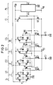
- the interconnection of the individual stages ST1 and ST2, their implementation and the implementation of the inverter stages I3 and I4 is to be carried out as in the two-stage voltage multiplication circuit according to FIG. 1.
- the same components as in FIG. 1 are provided with the same reference symbols in the four-stage embodiment of the voltage multiplication circuit.
- the structure of the third and fourth stages ST3 and ST4 is similar to the first two stages ST1 and ST2.
- the third stage ST3 contains an inverter stage I5, a capacitor C4 and two n-channel field effect transistors N8 and N9.
- a first connection of the fourth capacitance C4 is connected to an output of the fifth inverter stage I5 and to a second connection via the eighth n-channel field effect transistor N8 to the second reference potential V SS .
- the substrate connection of the eighth n-channel field effect transistor N8 is also connected to the second connection of the capacitance C4.
- the ninth n-channel field effect transistor N9 is connected between the third reference potential V KK , which represents the most negative voltage in the circuit of FIG.
- the substrate connection of the ninth n-channel field effect transistor N9 also is connected to V KK .
- the inverter stage I5 is again built using two complementary field effect transistors P7 and N15, a first connection of P7 and N15 forming the output of the inverter stage I5 and the gate connections of both field effect transistors representing the input of the fifth inverter stage I5, which on the one hand is connected to the gate connections of the n Channel field-effect transistor N3, the n-channel field-effect transistor N9 and the n-channel field-effect transistor N2 is connected to the output of the fifth inverter stage I3.
- the inverter stage I5 is between the first reference potential V DD and the second reference potential V SS connected, the second connection and the substrate connection of the p-channel field-effect transistor P7 being connected to the first reference potential V DD and the substrate connection and second connection of the N-channel field-effect transistor N15 being connected to the second reference potential V SS .
- the structure of the fourth stage ST4 connected to the third stage ST3 is similar. It consists of the sixth inverter stage I6, the fifth capacitor C5 and the two n-channel field effect transistors N10 and N11.
- the first connection of the capacitance C5 is in turn connected to the output of the sixth inverter stage I6 and the second connection of the capacitance C5 is connected to the first reference potential V SS via the tenth n-channel field effect transistor N10.
- the substrate connection is also connected to the second connection of the capacitance C5 and the second connection is connected to the third reference potential V KK via the n-channel field effect transistor N11.
- the substrate connection of the same field effect transistor is also connected to the third reference potential V KK .
- a capacitance C3 which is analog in the first and second stages represents the capacitance C6 for the two stages ST3 and ST4, which is connected between the ground GND and the third reference potential V KK .
- the sixth inverter stage I6 contains an n- and a p-channel field effect transistors P8 and N16, the substrate connection and the first connection of N16 being connected to the second reference potential V SS and the first connection and substrate connection of P8 being connected to the first reference potential V DD .
- the two gate connections of P8 and N16 are to be connected to the gate connection of the eighth n-channel field effect transistor N8 and to the gate connections of N1, N4 and N11.
- the output of the sixth inverter stage I6 is formed from the second connection of P8 and N16 together.
- the gate connections have to be connected to the output of the third inverter stage I3 or to the clock output ⁇ A of the level converter. These transistors must be driven so that they are at a Lock voltage of -3 V DD safely. This is certainly the case if their gate connection is under the voltage of -3 x V DD + V TN lies (with V TN is again the threshold voltage of an n-channel field effect transistor).
- the input of the sixth inverter stage I6 is also connected to the clock output ⁇ A of the level converter.
- the gate connection of the second n-channel field effect transistor N2 the gate connection of the third n-channel field effect transistor N3, the gate connection of the ninth and the tenth n-channel field effect transistor N9 and N10 are to be connected.
- the input of the fifth inverter stage I5 is also connected to the output of the third inverter stage I3.
- the output of this four-stage voltage multiplication circuit is to be connected to the third reference potential V KK , a voltage of V KK equal to - 3 ⁇ V DD occurring at this third reference potential.
- V KK a voltage of V KK equal to - 3 ⁇ V DD occurring at this third reference potential.
- the implementation of the level converter PU which is used in the voltage multiplier circuit according to FIG. 1 and FIG. 2, is now described in the following FIG. 3.
- the level converter PU according to FIG. 3 contains three n-channel field effect transistors N5, N6 and N7 as well as three p-channel field effect transistors P1, P2 and P3.
- the p-channel field effect transistor P3 and the n-channel field effect transistor N7 are connected as inverters and the two n-channel field effect transistors N5 and N6 form a bistable multivibrator.
- Field effect transistor P2 is in the conductive state because its gate connection is driven inversely with the same clock via the inverter stage formed by P3 and N7.
- the p-channel field effect transistor P3 conducts and the n-channel field effect transistor N7 blocks in this case.
- the gate terminal of the P2 field-effect transistor is therefore also connected to a positive voltage V DD and blocks the transistor.
- the positive voltage V DD is located at the clock output ⁇ A and at the gate connection of the n-channel field effect transistor N5. It conducts the n-channel field-effect transistor N5 and thereby blocks the sixth n-channel field-effect transistor N6, since the negative reference potential V SS or V KK is connected to its gate line. This results in a square-wave voltage at the clock output ⁇ A, which alternates in the clock of the square-wave voltage on the clock line between the first reference potential V DD and the respective second or third reference potential V SS , V KK .
- the level converter must be connected as follows.
- a first connection and a substrate connection of the fifth n-channel field effect transistor N5 and a first connection and substrate connection of the sixth n-channel field effect transistor N6 are common to the output of the voltage multiplication circuit or the second or third reference potential V SS , V KK connected and a gate terminal of the fifth n-channel field effect transistor N5, a second terminal of the sixth n-channel field effect transistor N6 and a first terminal of the first p-channel field effect transistor P1 together form the clock output ⁇ A of the level converter.
- a gate connection of the sixth n-channel field effect transistor N6 is to be connected to a second connection of the fifth n-channel field effect transistor N5 and to a first connection of the second p-channel field effect transistor P2, and a first connection and substrate connection of the seventh n-channel Field effect transistor must be connected to ground GND.
- a second connection of the same transistor is to be connected to the gate connection of the second p-channel field effect transistor P2 and a first connection of the third p-channel field effect transistor P3, and a second connection and substrate connection of the third p-channel field effect transistor P3, a second connection and The substrate connection of the second p-channel field effect transistor P2 and a second connection and substrate connection of the first p-channel field effect transistor P1 is to be connected to the first reference potential V DD .
- the control takes place via the clock line at the clock input ⁇ E, the gate connection of the third p-channel field effect transistor P3 and the gate connection of the seventh n-channel field effect transistor N7 having to be connected to the clock supply line.
Landscapes
- Engineering & Computer Science (AREA)
- Acoustics & Sound (AREA)
- Neurosurgery (AREA)
- Otolaryngology (AREA)
- Physics & Mathematics (AREA)
- General Health & Medical Sciences (AREA)
- Health & Medical Sciences (AREA)
- Signal Processing (AREA)
- Power Engineering (AREA)
- Dc-Dc Converters (AREA)
- Amplifiers (AREA)
- Filters That Use Time-Delay Elements (AREA)
- Networks Using Active Elements (AREA)
Claims (8)
- Circuit multiplicateur de tension à plusieurs étages comportant un premier convertisseur de niveau (PU) et un étage inverseur relié (I3), du type dans lequel le premier étage (ST1) du circuit multiplicateur de tension à plusieurs étages comporte une première capacité (C1), un premier étage inverseur (I1) et des premier et deuxième transistors à effet de champ (N1, N2) de premier type, et du type dans lequel une première borne de la première capacité (C1) est connectée à une sortie du premier étage inverseur (I1), et une seconde borne de la première capacité (C1) est reliée à la masse (GND), par l'intermédiaire du premier transistor à effet de champ de premier type (N1), et du type dans lequel la seconde borne de la première capacité (C1) est connectée, par l'intermédiaire du deuxième transistor à effet de champ de premier type (N2), à un second potentiel de référence (VSS), et le premier étage inverseur (I1) est branché entre le premier potentiel de référence (VDD) et la masse (GND), et du type dans lequel une entrée du premier étage inverseur (I1) forme une entrée du premier étage, une borne de grille du premier transistor à effet de champ de premier type (N1) forme une première entrée de commande, et une borne de grille du deuxième transistor à effet de champ de premier type (N2) forme une seconde entrée de commande du premier étage, et du type dans lequel une borne de substrat du premier transistor à effet de champ de premier type (N1) est connectée à la seconde borne de la première capacité (C1), et une borne de substrat du deuxième transistor à effet de champ de premier type (N2) est connectée au second potentiel de référence (VSS), caractérisé par le fait qu'un second étage comporte une deuxième capacité (C2), un deuxième étage inverseur (I2) ainsi que des troisième et quatrième transistors à effet de champ de premier type (N3, N4), qu'une première borne de la deuxième capacité (C2) est reliée à une sortie du deuxième étage inverseur (I2) et qu'une seconde borne de la deuxième capacité (C2) est connectée à la masse (GND), par l'intermédiaire du troisième transistor à effet de champ de premier type (N3), que la seconde borne de la deuxième capacité (C2) est reliée, par l'intermédiaire du quatrième transistor à effet de champ de premier type (N4) au second potentiel de référence (VSS) et que le deuxième étage inverseur (I2) est branché entre le premier potentiel de référence (VDD) et la masse (GND), qu'une entrée du deuxième étage inverseur (I2) forme une entrée du deuxième étage, une borne de grille du troisième transistor à effet de champ de premier type (N3) forme une troisième entrée de commande, et une borne de grille du quatrième transistor à effet de champ de premier type (N4) forme une quatrième entrée de commande, qu'une borne de substrat du troisième transistor à effet de champ de premier type (N3) est connectée à la seconde borne de la deuxième capacité (C2) et qu'une borne de substrat du quatrième transistor à effet de champ de premier type (N4) est reliée au second potentiel de référence (VSS), qu'une sortie de cadence (φA) du convertisseur de niveau (PU) est reliée à une entrée d'un troisième étage inverseur (I3) et aux première et quatrième entrées de commande, et que les deuxième et troisième entrées de commande sont reliées à une sortie du troisième étage inverseur (I3), que l'entrée du premier étage est reliée à une sortie d'un quatrième étage inverseur (I4) et que l'entrée du deuxième étage est reliée à une entrée du quatrième étage inverseur (I4) et à une entrée de cadence (φE) du convertisseur de niveau, que le quatrième étage inverseur (I4) est branché entre le premier potentiel de référence (VDD) et la masse (GND), et que l'entrée du quatrième étage inverseur (I4) forme une entrée de cadence (φ) du circuit multiplicateur de tension à plusieurs étages, que le troisième étage inverseur (I3) est branché entre la sortie du circuit multiplicateur de tension et le premier potentiel de référence (VDD), que le convertisseur de niveau (PU) est reliée aux premier et second potentiels de référence (VDD, VSS) et la masse (GND), et qu'une sortie du circuit multiplicateur de tension à deux étages est reliée au second potentiel de référence (VSS).
- Circuit multiplicateur de tension à plusieurs étages suivant la revendication 1, caractérisé par le fait qu'une troisième capacité (C3) utilisée pour le lissage est branchée entre la masse (GND) et le second potentiel de référence (VSS).
- Circuit multiplicateur de tension à plusieurs étages selon l'une des revendications 1 ou 2, caractérisé par le fait que les premier et deuxième étages (ST1, ST2) sont suivis par des troisième et quatrième étages (ST3, ST4), que les troisième et quatrième étages comportent des cinquième et sixième étages inverseurs (I5, I6), des huitième, neuvième, dixième et onzième transistors à effet de champ de premier type (N8, N9, N10 et N11), et des quatrième et cinquième capacités (C4, C5), que les deuxième et troisième entrées de commande sont reliées à une entrée du cinquième étage inverseur (I5) et que les première et quatrième bornes de commande sont reliées à une entrée du sixième étage inverseur (I6), que les cinquième et sixième étages inverseurs sont connectés respectivement entre le premier potentiel de référence (VDD) et le second potentiel de référence (VSS), que la quatrième capacité (C4) est reliée, par une première borne, à une sortie du cinquième étage inverseur (I5) et, par une seconde borne, par l'intermédiaire d'un huitième transistor à effet de champ de premier type (N8), au second potentiel de référence (VSS), et que la cinquième capacité (C5) est reliée, par une première borne, à une sortie du sixième étage inverseur (I6) et, par une seconde borne, par l'intermédiaire du dixième transistor à effet de champ de premier type (N10), au second potentiel de référence (VSS), qu'une borne de substrat du huitième transistor à effet de champ de premier type (N8) est reliée à la seconde borne de la quatrième capacité (C4), et qu'une borne de substrat du dixième transistor à effet de champ de premier type (N10) est reliée à la seconde borne de la cinquième capacité (C5), que le neuvième transistor à effet de champ de premier type (N9) est branché entre la quatrième capacité (C4) et un troisième point de référence (VKK), et que le onzième transistor à effet de champ de premier type (N11) est branché entre la cinquième capacité (C5) et le troisième potentiel de référence (VKK), qu'une borne du substrat des neuvième et onzième transistors à effet de champ de premier type (N9, N11) est reliée au troisième potentiel de référence (VKK), qu'une borne de grille du huitième transistor à effet de champ de premier type (N8) et une borne de grille du onzième transistor à effet de champ de premier type (N11) sont reliés, en tant que cinquième et huitième bornes de commande, en commun à la sortie de cadence (φA) du convertisseur de niveau (PU) et que des bornes de grille respectives du neuvième transistor à effet de champ de premier type et du dixième à effet de champ de premier type (N9, N10) sont reliées, en tant que septième et huitième bornes de commande, en commun à la sortie du troisième étage inverseur (I3), et que la sortie du circuit multiplicateur de tension à quatre étages est reliée au troisième potentiel de référence (VKK).
- Circuit multiplicateur de tension suivant la revendication 3, caractérisé par le fait qu'une sixième capacité (C6) u tilisée pour le lissage est branchée entre la masse (GND) et le troisième potentiel de référence (VKK).
- Circuit multiplicateur de tension à plusieurs étages suivant l'une des revendications 1 à 4, caractérisé par le fait que le convertisseur de niveau (PU) comporte des cinquième, sixième et septième transistors à effet de champ de premier type (N5, N6, N7) et des premier, deuxième et troisième transistors à effet de champ (P1, P2, P3) de second type, qu'une première borne et une borne de substrat du cinquième transistor à effet de champ de premier type (N5) et une première borne et une borne de substrat du sixième transistor à effet de champ de premier type (N6) sont reliées à la sortie du circuit multiplicateur de tension à plusieurs étages, qu'une borne de grille du cinquième transistor à effet de champ de premier type (N5) et une seconde borne du sixième transistor à effet de champ de premier type (N6) et une borne du premier transistor à effet de champ de second type (P1) constituent la sortie (φA) du convertisseur de niveau (PU), qu'une borne de grille du sixième transistor à effet de champ de premier type (N6) peut être reliée à une seconde borne du cinquième transistor à effet de champ de premier type (N5) et à une première borne du deuxième transistor à effet de champ de second type (P2), qu' une première borne et une borne de substrat du septième transistor à effet de champ de premier type (N7) peut être reliée à la masse (GND) et qu'une seconde borne de ce même transistor peut être reliée à une borne de grille du deuxième transistor à effet de champ de second type (P2) et à une première borne du troisième transistor à effet de champ de second type (P3), qu'une seconde borne et une borne de substrat du troisième transistor à effet de champ de second type (P3), une seconde borne et une borne de substrat du deuxième transistor à effet de champ de second type (P2) et une seconde borne et une borne de substrat du premier transistor à effet de champ de second type (P1) sont reliées au premier potentiel de référence (VDD), et qu'une borne de grille du troisième transistor à effet de champ de second type (P3) et une borne de grille du septième transistor à effet de champ de premier type (N7) forment en commun l'entrée de cadence (φE) du convertisseur de niveau (PU).
- Circuit multiplicateur de tension à plusieurs étages suivant l'une des revendications 1 à 4, caractérisé par le fait que les étages inverseurs comportent un transistor à effet de champ de premier type et un transistor à effet de champ de second type, qu'une borne de grille du transistor à effet de champ de premier type et une borne de grille du transistor à effet de champ de second type forment l'entrée du circuit inverseur, qu'une première borne du transistor à effet de champ de premier type et une première borne du transistor à effet de champ de second type forment en commun la sortie de l'étage inverseur, qu'une seconde borne et une borne de substrat du transistor à effet de champ de premier type sont reliées à la masse (GND) ou au second ou au troisième potentiel de référence (VSS, VKK), et qu'une seconde borne et une borne de substrat du transistor à effet de champ de second type peuvent être reliées au premier potentiel de référence (VDD).
- Circuit multiplicateur de tension à étages multiples suivant l'une des revendications 1 à 6, caractérisé par le fait que les transistors à effet de champ de premier type sont des transistors à effet de champ à canal n et que les transistors à effet de champ de second type sont des transistors à effet de champ à canal p, que le premier potentiel de référence (VDD) est une tension d'alimentation positive et que les second et troisième potentiels de référence (VSS, VKK) représentent une tension négative.
- Circuit multiplicateur de tension à plusieurs étages suivant l'une des revendications 1 à 6, caractérisé par le fait que les transistors à effet de champ de premier type sont des transistors à effet de champ à canal p et que les transistors à effet de champ de second type sont des transistors à effet de champ à canal n, que le premier potentiel de référence (VDD) est une tension d'alimentation négative et que les second et troisième potentiels de référence (VSS, VKK) représentent une tension positive.
Applications Claiming Priority (2)
| Application Number | Priority Date | Filing Date | Title |
|---|---|---|---|
| DE3834927 | 1988-10-13 | ||
| DE3834927 | 1988-10-13 |
Publications (3)
| Publication Number | Publication Date |
|---|---|
| EP0363715A2 EP0363715A2 (fr) | 1990-04-18 |
| EP0363715A3 EP0363715A3 (fr) | 1991-01-09 |
| EP0363715B1 true EP0363715B1 (fr) | 1994-06-01 |
Family
ID=6365066
Family Applications (1)
| Application Number | Title | Priority Date | Filing Date |
|---|---|---|---|
| EP89117649A Expired - Lifetime EP0363715B1 (fr) | 1988-10-13 | 1989-09-25 | Circuit multiplicateur de tension intégré pour alimentation de puissance basse tension |
Country Status (4)
| Country | Link |
|---|---|
| US (1) | US4982317A (fr) |
| EP (1) | EP0363715B1 (fr) |
| JP (1) | JP2807286B2 (fr) |
| DE (1) | DE58907764D1 (fr) |
Families Citing this family (17)
| Publication number | Priority date | Publication date | Assignee | Title |
|---|---|---|---|---|
| GB9007790D0 (en) * | 1990-04-06 | 1990-06-06 | Lines Valerie L | Dynamic memory wordline driver scheme |
| GB9007791D0 (en) * | 1990-04-06 | 1990-06-06 | Foss Richard C | High voltage boosted wordline supply charge pump and regulator for dram |
| US5500902A (en) * | 1994-07-08 | 1996-03-19 | Stockham, Jr.; Thomas G. | Hearing aid device incorporating signal processing techniques |
| US8085959B2 (en) * | 1994-07-08 | 2011-12-27 | Brigham Young University | Hearing compensation system incorporating signal processing techniques |
| EP0696839B1 (fr) * | 1994-08-12 | 1998-02-25 | Co.Ri.M.Me. Consorzio Per La Ricerca Sulla Microelettronica Nel Mezzogiorno | Elévateur de tension du type à pompage de charge |
| SE504371C2 (sv) * | 1995-02-28 | 1997-01-20 | Ericsson Telefon Ab L M | Anordning och förfarande i telekommunikationssystem för optisk spänningsmultiplicering i integrerad krets |
| US5606491A (en) * | 1995-06-05 | 1997-02-25 | Analog Devices, Inc. | Multiplying and inverting charge pump |
| US5815581A (en) * | 1995-10-19 | 1998-09-29 | Mitel Semiconductor, Inc. | Class D hearing aid amplifier with feedback |
| US5838807A (en) * | 1995-10-19 | 1998-11-17 | Mitel Semiconductor, Inc. | Trimmable variable compression amplifier for hearing aid |
| GB2332793A (en) * | 1997-12-24 | 1999-06-30 | Ericsson Telefon Ab L M | Voltage doubling circuit for MOS transistor gate drive |
| US6271715B1 (en) | 1998-02-27 | 2001-08-07 | Maxim Integrated Products, Inc. | Boosting circuit with supply-dependent gain |
| US6424208B1 (en) | 1999-12-30 | 2002-07-23 | The Engineering Consortium, Inc. | Switched capacitor filter with integrated voltage multiplier |
| US6310556B1 (en) | 2000-02-14 | 2001-10-30 | Sonic Innovations, Inc. | Apparatus and method for detecting a low-battery power condition and generating a user perceptible warning |
| US7443836B2 (en) * | 2003-06-16 | 2008-10-28 | Intel Corporation | Processing a data packet |
| US20080003462A1 (en) * | 2006-06-29 | 2008-01-03 | More Energy Ltd. | Digital logic control DC-to-DC converter with controlled input voltage and controlled power output |
| US10715834B2 (en) | 2007-05-10 | 2020-07-14 | Interdigital Vc Holdings, Inc. | Film grain simulation based on pre-computed transform coefficients |
| CN102096431B (zh) * | 2010-12-27 | 2012-08-15 | 上海贝岭股份有限公司 | 一种cmos电压倍增电路 |
Family Cites Families (17)
| Publication number | Priority date | Publication date | Assignee | Title |
|---|---|---|---|---|
| GB1348285A (en) * | 1971-07-26 | 1974-03-13 | Integrated Photomatrix Ltd | Voltage generator |
| GB1364618A (en) * | 1971-12-03 | 1974-08-21 | Seiko Instr & Electronics | Voltage boosters |
| JPS6028232B2 (ja) * | 1975-08-14 | 1985-07-03 | シャープ株式会社 | Dc−dcコンバ−タ |
| IT1073440B (it) * | 1975-09-22 | 1985-04-17 | Seiko Instr & Electronics | Circuito elevatore di tensione realizzato in mos-fet |
| US4106086A (en) * | 1976-12-29 | 1978-08-08 | Rca Corporation | Voltage multiplier circuit |
| US4199806A (en) * | 1978-01-18 | 1980-04-22 | Harris Corporation | CMOS Voltage multiplier |
| DE2821418A1 (de) * | 1978-05-16 | 1979-11-22 | Siemens Ag | Taktgesteuerter gleichspannungswandler |
| US4302804A (en) * | 1979-09-04 | 1981-11-24 | Burroughs Corporation | DC Voltage multiplier using phase-sequenced CMOS switches |
| US4344003A (en) * | 1980-08-04 | 1982-08-10 | Rca Corporation | Low power voltage multiplier circuit |
| US4321661A (en) * | 1980-12-23 | 1982-03-23 | Gte Laboratories Incorporated | Apparatus for charging a capacitor |
| US4460952A (en) * | 1982-05-13 | 1984-07-17 | Texas Instruments Incorporated | Electronic rectifier/multiplier/level shifter |
| DE3335423A1 (de) * | 1983-09-29 | 1985-04-04 | Siemens AG, 1000 Berlin und 8000 München | Schaltung zur spannungsvervielfachung |
| US4663701A (en) * | 1985-08-02 | 1987-05-05 | Intermedics, Inc. | Voltage level shifter |
| US4621315A (en) * | 1985-09-03 | 1986-11-04 | Motorola, Inc. | Recirculating MOS charge pump |
| US4636930A (en) * | 1985-10-01 | 1987-01-13 | Maxim Integrated Products, Inc. | Integrated dual charge pump power supply and RS-232 transmitter/receiver |
| FR2611283B1 (fr) * | 1987-02-19 | 1989-06-09 | Em Microelectronic Marin Sa | Dispositif comportant un circuit electronique de traitement d'un signal analogique |
| JPS63290159A (ja) * | 1987-05-20 | 1988-11-28 | Matsushita Electric Ind Co Ltd | 昇圧回路 |
-
1989
- 1989-09-25 US US07/411,923 patent/US4982317A/en not_active Expired - Lifetime
- 1989-09-25 DE DE58907764T patent/DE58907764D1/de not_active Expired - Fee Related
- 1989-09-25 EP EP89117649A patent/EP0363715B1/fr not_active Expired - Lifetime
- 1989-10-11 JP JP1266058A patent/JP2807286B2/ja not_active Expired - Fee Related
Also Published As
| Publication number | Publication date |
|---|---|
| EP0363715A3 (fr) | 1991-01-09 |
| DE58907764D1 (de) | 1994-07-07 |
| US4982317A (en) | 1991-01-01 |
| EP0363715A2 (fr) | 1990-04-18 |
| JP2807286B2 (ja) | 1998-10-08 |
| JPH02256309A (ja) | 1990-10-17 |
Similar Documents
| Publication | Publication Date | Title |
|---|---|---|
| DE69111113T2 (de) | Kondensator-Ladungspumpen. | |
| DE69319512T2 (de) | Spannungswandlerschaltung | |
| DE3879804T2 (de) | Integrierte halbleiterschaltungsvorrichtung. | |
| EP0389846B1 (fr) | Circuit multiplicateur de tension | |
| DE69514090T2 (de) | Oszillatorschaltung mit einer versorgungsspannungsunabhängigen Oszillatorfrequenz | |
| EP0135889B1 (fr) | Circuit de multiplication de tension | |
| DE69111499T2 (de) | Ladungspumpvorrichtung. | |
| DE19930394B4 (de) | Geschaltete Abwärts- und Aufwärts-Kondensatorverstärkungsstufe mit optionalem gemeinschaftlichem Ruhezustand | |
| DE602004008935T2 (de) | Flächeneffiziente ladungspumpe | |
| DE2642431C2 (fr) | ||
| EP0363715A2 (fr) | Circuit multiplicateur de tension intégré pour alimentation de puissance basse tension | |
| DE69422164T2 (de) | Kapazitive Ladungspumpe, Bicmos Schaltung für niedrige Versorgungsspannung | |
| DE69408665T2 (de) | Spannungserhöher vom Ladungspumpentype | |
| EP0300560B1 (fr) | Circuit de comparison | |
| DE102005012662B4 (de) | Anordnung mit Spannungskonverter zur Spannungsversorgung einer elektrischen Last und Verfahren zur Spannungsversorgung einer elektrischen Last | |
| WO2000038303A1 (fr) | Dispositif de multiplication de tension de haut rendement et son utilisation | |
| DE2525075A1 (de) | Spannungsvervielfacherschaltung | |
| DE69720128T2 (de) | Schneller, verbrauchsarmer Chopper Komparator mit störungsfreier Funktion bei Variation des logischen Schwellwertes der Inverter | |
| EP0633662B1 (fr) | Montage pour un oscillateur en anneau | |
| DE69226021T2 (de) | Treiberschaltung für einen elektronischen Schalter | |
| DE60201778T2 (de) | Spannungskomparatorschaltung | |
| DE69406857T2 (de) | Schnittstellenschaltung und diese Schaltung enthaltende Spannungserhöhungsschaltung | |
| DE69416554T2 (de) | Ringoszillatorschaltung für spannungsgesteuerten Oszillator mit frequenzunabhängigem Tastverhältnis | |
| DE69721940T2 (de) | Pegelverschiebungsschaltung | |
| DE69113414T2 (de) | Integrierte Konstantstromversorgung. |
Legal Events
| Date | Code | Title | Description |
|---|---|---|---|
| PUAI | Public reference made under article 153(3) epc to a published international application that has entered the european phase |
Free format text: ORIGINAL CODE: 0009012 |
|
| AK | Designated contracting states |
Kind code of ref document: A2 Designated state(s): CH DE FR GB IT LI |
|
| PUAL | Search report despatched |
Free format text: ORIGINAL CODE: 0009013 |
|
| AK | Designated contracting states |
Kind code of ref document: A3 Designated state(s): CH DE FR GB IT LI |
|
| 17P | Request for examination filed |
Effective date: 19901205 |
|
| 17Q | First examination report despatched |
Effective date: 19921117 |
|
| GRAA | (expected) grant |
Free format text: ORIGINAL CODE: 0009210 |
|
| AK | Designated contracting states |
Kind code of ref document: B1 Designated state(s): CH DE FR GB IT LI |
|
| REF | Corresponds to: |
Ref document number: 58907764 Country of ref document: DE Date of ref document: 19940707 |
|
| ITF | It: translation for a ep patent filed | ||
| GBT | Gb: translation of ep patent filed (gb section 77(6)(a)/1977) |
Effective date: 19940811 |
|
| ET | Fr: translation filed | ||
| PLBE | No opposition filed within time limit |
Free format text: ORIGINAL CODE: 0009261 |
|
| STAA | Information on the status of an ep patent application or granted ep patent |
Free format text: STATUS: NO OPPOSITION FILED WITHIN TIME LIMIT |
|
| 26N | No opposition filed | ||
| REG | Reference to a national code |
Ref country code: GB Ref legal event code: IF02 |
|
| PGFP | Annual fee paid to national office [announced via postgrant information from national office to epo] |
Ref country code: DE Payment date: 20021118 Year of fee payment: 14 |
|
| PGFP | Annual fee paid to national office [announced via postgrant information from national office to epo] |
Ref country code: GB Payment date: 20030827 Year of fee payment: 15 |
|
| PGFP | Annual fee paid to national office [announced via postgrant information from national office to epo] |
Ref country code: CH Payment date: 20030901 Year of fee payment: 15 |
|
| PGFP | Annual fee paid to national office [announced via postgrant information from national office to epo] |
Ref country code: FR Payment date: 20030904 Year of fee payment: 15 |
|
| PG25 | Lapsed in a contracting state [announced via postgrant information from national office to epo] |
Ref country code: DE Free format text: LAPSE BECAUSE OF NON-PAYMENT OF DUE FEES Effective date: 20040401 |
|
| PG25 | Lapsed in a contracting state [announced via postgrant information from national office to epo] |
Ref country code: GB Free format text: LAPSE BECAUSE OF NON-PAYMENT OF DUE FEES Effective date: 20040925 |
|
| PG25 | Lapsed in a contracting state [announced via postgrant information from national office to epo] |
Ref country code: LI Free format text: LAPSE BECAUSE OF NON-PAYMENT OF DUE FEES Effective date: 20040930 Ref country code: CH Free format text: LAPSE BECAUSE OF NON-PAYMENT OF DUE FEES Effective date: 20040930 |
|
| REG | Reference to a national code |
Ref country code: CH Ref legal event code: PL |
|
| GBPC | Gb: european patent ceased through non-payment of renewal fee |
Effective date: 20040925 |
|
| PG25 | Lapsed in a contracting state [announced via postgrant information from national office to epo] |
Ref country code: FR Free format text: LAPSE BECAUSE OF NON-PAYMENT OF DUE FEES Effective date: 20050531 |
|
| REG | Reference to a national code |
Ref country code: FR Ref legal event code: ST |
|
| PG25 | Lapsed in a contracting state [announced via postgrant information from national office to epo] |
Ref country code: IT Free format text: LAPSE BECAUSE OF NON-PAYMENT OF DUE FEES Effective date: 20050925 |