EP0364056A2 - Condensateur de découplage monté en surface - Google Patents
Condensateur de découplage monté en surface Download PDFInfo
- Publication number
- EP0364056A2 EP0364056A2 EP89202587A EP89202587A EP0364056A2 EP 0364056 A2 EP0364056 A2 EP 0364056A2 EP 89202587 A EP89202587 A EP 89202587A EP 89202587 A EP89202587 A EP 89202587A EP 0364056 A2 EP0364056 A2 EP 0364056A2
- Authority
- EP
- European Patent Office
- Prior art keywords
- contacts
- board
- pair
- capacitor
- substrate
- Prior art date
- Legal status (The legal status is an assumption and is not a legal conclusion. Google has not performed a legal analysis and makes no representation as to the accuracy of the status listed.)
- Ceased
Links
Images
Classifications
-
- H—ELECTRICITY
- H01—ELECTRIC ELEMENTS
- H01G—CAPACITORS; CAPACITORS, RECTIFIERS, DETECTORS, SWITCHING DEVICES, LIGHT-SENSITIVE OR TEMPERATURE-SENSITIVE DEVICES OF THE ELECTROLYTIC TYPE
- H01G2/00—Details of capacitors not covered by a single one of groups H01G4/00-H01G11/00
- H01G2/02—Mountings
- H01G2/06—Mountings specially adapted for mounting on a printed-circuit support
- H01G2/065—Mountings specially adapted for mounting on a printed-circuit support for surface mounting, e.g. chip capacitors
-
- H—ELECTRICITY
- H01—ELECTRIC ELEMENTS
- H01G—CAPACITORS; CAPACITORS, RECTIFIERS, DETECTORS, SWITCHING DEVICES, LIGHT-SENSITIVE OR TEMPERATURE-SENSITIVE DEVICES OF THE ELECTROLYTIC TYPE
- H01G4/00—Fixed capacitors; Processes of their manufacture
- H01G4/35—Feed-through capacitors or anti-noise capacitors
-
- H—ELECTRICITY
- H01—ELECTRIC ELEMENTS
- H01G—CAPACITORS; CAPACITORS, RECTIFIERS, DETECTORS, SWITCHING DEVICES, LIGHT-SENSITIVE OR TEMPERATURE-SENSITIVE DEVICES OF THE ELECTROLYTIC TYPE
- H01G4/00—Fixed capacitors; Processes of their manufacture
- H01G4/40—Structural combinations of fixed capacitors with other electric elements, the structure mainly consisting of a capacitor, e.g. RC combinations
-
- H—ELECTRICITY
- H05—ELECTRIC TECHNIQUES NOT OTHERWISE PROVIDED FOR
- H05K—PRINTED CIRCUITS; CASINGS OR CONSTRUCTIONAL DETAILS OF ELECTRIC APPARATUS; MANUFACTURE OF ASSEMBLAGES OF ELECTRICAL COMPONENTS
- H05K1/00—Printed circuits
- H05K1/02—Details
- H05K1/0213—Electrical arrangements not otherwise provided for
- H05K1/0216—Reduction of cross-talk, noise or electromagnetic interference
- H05K1/023—Reduction of cross-talk, noise or electromagnetic interference using auxiliary mounted passive components or auxiliary substances
- H05K1/0231—Capacitors or dielectric substances
-
- H—ELECTRICITY
- H05—ELECTRIC TECHNIQUES NOT OTHERWISE PROVIDED FOR
- H05K—PRINTED CIRCUITS; CASINGS OR CONSTRUCTIONAL DETAILS OF ELECTRIC APPARATUS; MANUFACTURE OF ASSEMBLAGES OF ELECTRICAL COMPONENTS
- H05K1/00—Printed circuits
- H05K1/02—Details
- H05K1/14—Structural association of two or more printed circuits
- H05K1/141—One or more single auxiliary printed circuits mounted on a main printed circuit, e.g. modules, adapters
-
- H—ELECTRICITY
- H05—ELECTRIC TECHNIQUES NOT OTHERWISE PROVIDED FOR
- H05K—PRINTED CIRCUITS; CASINGS OR CONSTRUCTIONAL DETAILS OF ELECTRIC APPARATUS; MANUFACTURE OF ASSEMBLAGES OF ELECTRICAL COMPONENTS
- H05K7/00—Constructional details common to different types of electric apparatus
- H05K7/02—Arrangements of circuit components or wiring on supporting structure
- H05K7/10—Plug-in assemblages of components, e.g. IC sockets
- H05K7/1092—Plug-in assemblages of components, e.g. IC sockets with built-in components, e.g. intelligent sockets
-
- H—ELECTRICITY
- H10—SEMICONDUCTOR DEVICES; ELECTRIC SOLID-STATE DEVICES NOT OTHERWISE PROVIDED FOR
- H10W—GENERIC PACKAGES, INTERCONNECTIONS, CONNECTORS OR OTHER CONSTRUCTIONAL DETAILS OF DEVICES COVERED BY CLASS H10
- H10W44/00—Electrical arrangements for controlling or matching impedance
- H10W44/601—Capacitive arrangements
-
- H—ELECTRICITY
- H05—ELECTRIC TECHNIQUES NOT OTHERWISE PROVIDED FOR
- H05K—PRINTED CIRCUITS; CASINGS OR CONSTRUCTIONAL DETAILS OF ELECTRIC APPARATUS; MANUFACTURE OF ASSEMBLAGES OF ELECTRICAL COMPONENTS
- H05K2201/00—Indexing scheme relating to printed circuits covered by H05K1/00
- H05K2201/04—Assemblies of printed circuits
- H05K2201/049—PCB for one component, e.g. for mounting onto mother PCB
-
- H—ELECTRICITY
- H05—ELECTRIC TECHNIQUES NOT OTHERWISE PROVIDED FOR
- H05K—PRINTED CIRCUITS; CASINGS OR CONSTRUCTIONAL DETAILS OF ELECTRIC APPARATUS; MANUFACTURE OF ASSEMBLAGES OF ELECTRICAL COMPONENTS
- H05K2201/00—Indexing scheme relating to printed circuits covered by H05K1/00
- H05K2201/10—Details of components or other objects attached to or integrated in a printed circuit board
- H05K2201/10227—Other objects, e.g. metallic pieces
- H05K2201/10333—Individual female type metallic connector elements
-
- H—ELECTRICITY
- H05—ELECTRIC TECHNIQUES NOT OTHERWISE PROVIDED FOR
- H05K—PRINTED CIRCUITS; CASINGS OR CONSTRUCTIONAL DETAILS OF ELECTRIC APPARATUS; MANUFACTURE OF ASSEMBLAGES OF ELECTRICAL COMPONENTS
- H05K2201/00—Indexing scheme relating to printed circuits covered by H05K1/00
- H05K2201/10—Details of components or other objects attached to or integrated in a printed circuit board
- H05K2201/10431—Details of mounted components
- H05K2201/10507—Involving several components
- H05K2201/10515—Stacked components
-
- H—ELECTRICITY
- H05—ELECTRIC TECHNIQUES NOT OTHERWISE PROVIDED FOR
- H05K—PRINTED CIRCUITS; CASINGS OR CONSTRUCTIONAL DETAILS OF ELECTRIC APPARATUS; MANUFACTURE OF ASSEMBLAGES OF ELECTRICAL COMPONENTS
- H05K2201/00—Indexing scheme relating to printed circuits covered by H05K1/00
- H05K2201/10—Details of components or other objects attached to or integrated in a printed circuit board
- H05K2201/10613—Details of electrical connections of non-printed components, e.g. special leads
- H05K2201/10621—Components characterised by their electrical contacts
- H05K2201/10636—Leadless chip, e.g. chip capacitor or resistor
-
- H—ELECTRICITY
- H05—ELECTRIC TECHNIQUES NOT OTHERWISE PROVIDED FOR
- H05K—PRINTED CIRCUITS; CASINGS OR CONSTRUCTIONAL DETAILS OF ELECTRIC APPARATUS; MANUFACTURE OF ASSEMBLAGES OF ELECTRICAL COMPONENTS
- H05K2201/00—Indexing scheme relating to printed circuits covered by H05K1/00
- H05K2201/10—Details of components or other objects attached to or integrated in a printed circuit board
- H05K2201/10613—Details of electrical connections of non-printed components, e.g. special leads
- H05K2201/10621—Components characterised by their electrical contacts
- H05K2201/10689—Leaded Integrated Circuit [IC] package, e.g. dual-in-line [DIL]
-
- H—ELECTRICITY
- H05—ELECTRIC TECHNIQUES NOT OTHERWISE PROVIDED FOR
- H05K—PRINTED CIRCUITS; CASINGS OR CONSTRUCTIONAL DETAILS OF ELECTRIC APPARATUS; MANUFACTURE OF ASSEMBLAGES OF ELECTRICAL COMPONENTS
- H05K2201/00—Indexing scheme relating to printed circuits covered by H05K1/00
- H05K2201/10—Details of components or other objects attached to or integrated in a printed circuit board
- H05K2201/10613—Details of electrical connections of non-printed components, e.g. special leads
- H05K2201/10742—Details of leads
- H05K2201/10886—Other details
- H05K2201/10939—Lead of component used as a connector
-
- H—ELECTRICITY
- H05—ELECTRIC TECHNIQUES NOT OTHERWISE PROVIDED FOR
- H05K—PRINTED CIRCUITS; CASINGS OR CONSTRUCTIONAL DETAILS OF ELECTRIC APPARATUS; MANUFACTURE OF ASSEMBLAGES OF ELECTRICAL COMPONENTS
- H05K3/00—Apparatus or processes for manufacturing printed circuits
- H05K3/30—Assembling printed circuits with electric components, e.g. with resistors
- H05K3/32—Assembling printed circuits with electric components, e.g. with resistors electrically connecting electric components or wires to printed circuits
- H05K3/34—Assembling printed circuits with electric components, e.g. with resistors electrically connecting electric components or wires to printed circuits by soldering
- H05K3/3447—Lead-in-hole components
-
- H—ELECTRICITY
- H05—ELECTRIC TECHNIQUES NOT OTHERWISE PROVIDED FOR
- H05K—PRINTED CIRCUITS; CASINGS OR CONSTRUCTIONAL DETAILS OF ELECTRIC APPARATUS; MANUFACTURE OF ASSEMBLAGES OF ELECTRICAL COMPONENTS
- H05K3/00—Apparatus or processes for manufacturing printed circuits
- H05K3/36—Assembling printed circuits with other printed circuits
- H05K3/368—Assembling printed circuits with other printed circuits parallel to each other
-
- Y—GENERAL TAGGING OF NEW TECHNOLOGICAL DEVELOPMENTS; GENERAL TAGGING OF CROSS-SECTIONAL TECHNOLOGIES SPANNING OVER SEVERAL SECTIONS OF THE IPC; TECHNICAL SUBJECTS COVERED BY FORMER USPC CROSS-REFERENCE ART COLLECTIONS [XRACs] AND DIGESTS
- Y02—TECHNOLOGIES OR APPLICATIONS FOR MITIGATION OR ADAPTATION AGAINST CLIMATE CHANGE
- Y02P—CLIMATE CHANGE MITIGATION TECHNOLOGIES IN THE PRODUCTION OR PROCESSING OF GOODS
- Y02P70/00—Climate change mitigation technologies in the production process for final industrial or consumer products
- Y02P70/50—Manufacturing or production processes characterised by the final manufactured product
Definitions
- This invention is directed to a capacitor filter providing a low impedance and low inductance decoupling loop to reduce circuit voltage noise for insertion into a printed circuit (PC) board with redesign or special socketing of the PC board.
- the invention finds particularly utility with standard dual-in-line packaged (DIP) integrated circuits.
- auxiliary boards have a relatively high height which can interfere with clearance requirements of the PC board or are relatively expensive items.
- items (2) and (3) require the use of from 6 to 48 relatively expensive sockets on each auxiliary board with attendant high assembly costs.
- the present invention allows inexpensive decoupling of all IC positions on a PC board without redesign or special socketing on existing production boards. On a new PC board product it saves costs and layout time with increased package density on the PC board or results in a smaller PC board size. It is simple to install and has no easily bendable parts which can cause misalignment problems during hand or automatic insertion on a PC board.
- the present invention is a surface mounted device compatible with the latest surface mount technology.
- This invention involves an improvement in capacitor filters for use with integrated circuit (IC) packages and the printed circuit (PC) boards into which the packages are inserted.
- a relatively inexpensive auxiliary board of an overall size including particularly a small overall thickness is provided, which permits the capacitor-containing board to be positioned between the underside of dual-in-line (DIP) IC Package and the PC board into which the DIP is plugged.
- the auxiliary board thus is positioned within the same PC board space (area) as the DIP with which it is associated. Thus, there is no space penalty in utilizing this auxiliary capacitor board. No redesign or additional socketing of the PC board is necessary.
- the capacitor board may be mounted in an alternative configuration on the underside of the PC board where it can contact the protruding leads of a DIP package inserted into sockets accessed on the top of the PC board.
- a bare minimum of parts are used in construction which makes for an inexpensive device and one which can be easily and reliably inserted by automatic insertion means into the PC board or on the DIP package leads.
- auxiliary board of a substantially rectangular shape with integral end tabs extending from opposite corners on opposite ends of the board.
- Two serpentine metallic traces are deposited on the board extending from apertures formed in the two tabs to a central board location at which position a decoupling capacitor is mounted and electrically connected to the traces.
- a single pair of hollow electrical insertable contacts are mounted in the tab apertures which are spaced apart the same distance as the spacing of the two PC board sockets (typically a ground socket and a power source voltage socket).
- the pair of plug-in contacts contact the metal traces leading from the capacitor leads.
- two contacts are inserted into the two concerned sockets of the PC board so that the auxiliary board is flush with the PC board.
- the DIP package is then inserted over the auxiliary board so that appropriate power and ground leads of the DIP package are inserted into the interior of the two auxiliary board hollow contacts making connection through those contacts to the counterpart PC board sockets.
- the auxiliary capacitor board may be mounted on the underside of PC board by engaging the insertable contacts in the auxiliary board tabs with the underside of the appropriate PC board socket positions.
- the DIP leads are inserted into the PC board socket positions, i.e. holes, from the top component side of the PC board. Two of the DIP leads protruding from the bottom side of the PC board pass into the center of the insertable contacts mounted in the auxiliary board tabs.
- auxiliary board In another embodiment four tabs are provided, one at each corner of a generally rectangular substrate (the auxiliary board) which then has the outline of a flat H-shape or a block I dependent on orthogonal orientation.
- Contacts are positioned on two diametrical opposed tabs or legs with clearance holes (non-plated through) on the other two diametrically opposed tabs or legs.
- Power and ground leads from the DIP package pass into electrical connection with the pair of contacts while two other leads of the DIP pass through the clearance holes without any electrical contact and into two of the remaining sockets of the printed circuit board aligned with the clearance holes of the decoupling assembly.
- the remainder of the DIP leads pass past the auxiliary board to the still remaining sockets of the PC board.
- two spaced pairs of contacts are provided on opposite sides of the auxiliary board or insulative substrate, which has a block L-shape with a first pair of contacts on a vertical margin of the L-shape and connected respectively to opposed sideplates of a first decoupling capacitor, and a second pair of contacts on a vertical margin of the L-shape base which are connected respectively to opposed sideplates of a second decoupling capacitor.
- a first DIP power lead and a first DIP ground lead are simultaneously inserted into one of the edge pairs of contacts and a second DIP power lead and a second DIP ground lead are inserted into the opposed spaced other pair of contacts. This provides a pair of decoupling capacitors resulting in a redundant decoupling capability.
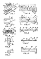
- a dual-in-line (DIP) integrated circuit package 11 is normally insertable into a series of sockets 16a through 16x and 17a through 17x in a printed circuit (PC) board 12.
- the number of DIP terminal leads 14a through 14x and 15a through 15x on the DIP may range from 8 to 16 to 24 to 48 or more pins.
- Leads of the series of leads 15a through 15x, other than lead 15a, are not shown in the drawing since they are obscured in the view presented. They extend parallel to leads 14a through 14x and are inserted into sockets 17a through 17x of the printed circuit board.
- auxiliary capacitor board 20 with a single pair of hollow insertable contacts is provided which is insertable into two selected sockets 16x and 17a of the PC board 12.
- the auxiliary capacitor board 20 is mounted flush with PC board 12 so that a minimum height space is taken up by the auxiliary capacitor board.
- auxiliary capacitor board Details of the auxiliary capacitor board are seen in Figures 3-10 below.
- the DIP package After insertion of the auxiliary capacitor board into the appropriate ground and power sockets of the PC board, the DIP package is inserted into the corresponding sockets of socket 16a through 16x and 17a through 17x of the PC board by insertion of the DIP leads 14a through 14x and 15a through 15x into the corresponding sockets.
- DIP leads 15a and 14x as shown will be insertable into socket 17a and 16x by passage through the internal fingers of the pair of hollow insertable contacts contained in the auxiliary capacitor board.
- FIG. 2 illustrates in simplified form the schematic electrical circuit involved.
- Lead 14x′ and lead 15a′ of the integrated circuit chip 21 are connected respectfully to ground 23 and a voltage source 22.
- a capacitor 24 Connected between the voltage source and ground is a capacitor 24.
- Capacitor 24 functions to reduce voltage noise spikes and by that action can cut noise up to a factor of 10.
- FIG. 3 illustrates the initial fabrication steps involved in fabrication of the auxiliary decoupling capacitor board.
- a substrate board 30 is provided of suitable insulative board material such as 0.020 ⁇ 0.0030 FR-4 per Mil Spec P-055617 and Mil P-13949G which is an electrolytic copper clad (1 oz. one side) epoxy fiberglass insulation.
- notches 19 are routed out of an overall board containing a multiplicity of auxiliary board units to form substrate square tabs 31 and 32 extending integrally from opposite corners of opposite sides of the board 30.
- An aperture 36 is drilled or punched in each tab at a spacing S (Fig.
- auxiliary capacitor board 30 corresponding to the distance between opposed terminal leads of the DIP package to be mounted on the auxiliary capacitor board 30, e.g. the distance between leads 14a and 15a (Fig. 1).
- the width W of board 30 between the tabs is less than the distance between the oppositely arranged sets of terminal leads extending from the DIP package.
- the tabs and more particularly apertures 36 are located so that they are spaced apart a distance L representative of the linear distance between the particular DIP leads representing a ground lead and a power lead of the DIP package.
- Conductive metal traces 33 and 37 are deposited on the substrate 30 and extend from the aperture in each of the tabs 31 and 32 to spaced contacts 34 and 38 at a central portion of the auxiliary board 30.
- the metal traces may be of electrolytic copper plate in accord with specification Mil-F-55561.
- Contact plating at the areas of contact of the respective hollow insertable contacts 50 and 51 and for proper connection of the solder to the metal traces may be a tin/nickel or gold/nickel plating or may be pure tin or pure gold. These contacts await connection of a suitable plate capacitor.
- the ends 35 and 39 of each trace surround aperture 36 so that when contacts 50, 51 are inserted within the aperture an electrical connection is made between the contact and the respective traces.
- Capacitor 40 comprises a series of interdigitated plates 41 and 42 which form a spaced stack of capacitor plates.
- Metal sideplates 43 and 44 representing first and second capacitor leads connect each of the interdigitated sets of plates 41 and 42, respectively, so that each set of interdigitated plates are interconnected.
- the multi-layer ceramic capacitor stack is adhered to the auxiliary board substrate 30 by suitable adhesive 29 and/or solder 44a and 44b utilized to electrically connect sideplates 44 and 43, respectively, to contacts 34, 38 and traces 33 and 37, respectively.
- the overall maximum height of the capacitor is approximately from 0.040 to 0.050 inches.
- a suitable typical capacitor having utility in this invention is Model EIA 1206 manufactured by Kyocera Co.
- the insertable contacts 50 and 51 as shown in Figure 8 may be of the Model CM102 type, manufactured by Weiss-Aug. of New Brunswick, N.J.
- the insertable contacts of the auxiliary capacitor board extend from a side of board 30 opposite to the side of the board on which the capacitor 40 is mounted.
- the height C of the auxiliary capacitor board (and its capacitor) mounted flush to the top surface of the PC board is not more than about 0.070 inches.
- Such dimension minimizes the added height included by use of the auxiliary capacitor board while not interfering with a proper connection of the insertable contacts to the PC board sockets and to the plug-in of the appropriate pair of DIP terminal leads into the interior of insertable contacts 50 and 51.
- the critical dimension C is the aggregate of auxiliary board thickness and the ceramic capacitor height above the auxiliary board. In order to allow proper contact of the DIP terminal leads into the PC board sockets this dimension C must not be greater than about 0.070 inches.
- the overall height H of the auxiliary board including the capacitor and the insertable contacts is about 0.14 inches.
- Each of the insertable contacts 50, 51 typically of a 0.085 inch length are press-fitted into apertures 36 and are in electrical contact with trace ends 35 and 39 of the metal traces on the board 30 leading to opposite leads of capacitor 40.
- FIG. 7 shows an alternative embodiment in which contacts 50′ and 51′ extend outwardly from the same side of the board as the capacitor 40 is mounted and are connected at 55 to their respective metal traces 33 and 37 extending to the capacitor 40.
- the DIP package is inserted into the PC board from its top surface.
- the auxiliary capacitor board 20 is then plugged into the underside of the printed circuit board by contacts 50′ and 51′ insertable into the extended DIP pins coming through the PC board.
- the underside of the auxiliary capacitor board then may be wave soldered so that solder wicks up through the interior of the insertable contacts and solidifies the ends of the single pair of DIP terminal leads inserted in a gas-tight connection within the tines or flexible fingers of the insertable contacts 50′ and 51′. Solder also wicks into the other DIP leads inserted directly into the PC board sockets.
- a terminal contact of shorter length typically 0.065 inches long is preferred and the overall height of the capacitor board is decreased.
- Figures 8 and 9 illustrate the internal details of the insertable contacts.
- These contacts have a contact head 52 including an entrance 54, which head is insertable within the aperture 36 in each of the tabs and makes contact either within the aperture of 36 to a metal coated via or otherwise are electrically connected to their respective metal traces on the substrate 30.
- the insertable contacts 50, 51 typically made of beryllium copper 0.007 1/4 hard per specification QQ-C-533, contain four flexible fingers which taper to the aperture entrance 54 and engage the ends of the DIP terminal leads shown in Figure 1. A 6-9 oz. insertion force is normally required.
- Figure 10 shows an additional embodiment of the invention wherein the traces 33′ and 37′ on substrate 30 are nonserpentine.
- the capacitor may extend crosswise of the auxiliary board 30, i.e., along the S-axis.
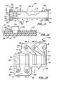
- Figures 11 and 12 show an embodiment 60 in which insulative substrate 61, typically of the same material as substrate 30 ( Figure 3), mounts at one end an interdigitated plate ceramic capacitor 40 of the type described above.
- the capacitor utilized conforms to Mil-C-55681B and has a value of 0.01 mf 50 v. ⁇ 20% or 0.33 mf 50 v. ⁇ 20% or 0.10 mf 50 v. ⁇ 20%, dependent on case size and application.
- a commercially available low profile capacitor used is sold by NOVACAP, Inc. under the trademark NOVACAP #1206 Z 104 M500 NTX.
- the substrate has a flat H-shape in the view shown (a block-I in an orthogonal direction) resultant from tabs 62, 63, 64 and 65 at each corner of an otherwise rectangular substrate.
- the substrate is screened with a soldermask maskant such as Dynachem PC 501, as is known in the art over a plane of 0.0014 inch thick 1 oz. copper coated on the substrate 61. Non-masked contact pad areas and an area of copper to be etched are provided as hereafter described.
- a first voltage plane 70 of the copper forming a first conductive pathway extends from one sideplate 43 of capacitor 40 to a first contact 66 in tab or leg 62.
- a second ground plane 71 of the copper forming a second conductive pathway extends from sideplate 44 along the substrate 61 to a second contact 67 in tab or leg 64.
- Contact pads 72a and 72b are tin-lead solder plated (Gyrex Reflow per Mil 55110-D) on the voltage plane 70 and ground plane 71 above tabs 62, 64, respectively, for reception of contacts 66, 67.
- Solder paste 44a, 44b (Mil QQS-571E) as seen in Figure 5 is utilized to connect the respective capacitor side plates to rectangular solder coated copper voltage and ground plane pads 72c and 72d, respectively.
- the voltage and ground planes are separated by an etched out area 75 of the copper extending from orthogonal edges of the copper and between pads 72c and 72d.
- Soldermask maskant 73 extends over the outboard edges of the voltage and ground planes and the areas around pads 72a-d.
- Contacts 66, 67 correspond to and are of the same design as plug-in contacts 50, 51 in Fig. 6.
- Clearance holes 68, 69 are formed in other tabs or legs 63, 65, respectively.
- a DIP or other IC power pin and ground pin are inserted into electrical connection with contacts 66, 67, respectively, while two other DIP pins merely freely pass through clearance holes 68, 69 without electrical connection therewith and into aligned sockets in a printed circuit board.
- the remaining DIP pins extend in a straight line as indicated by + positions 59 between the apertures in tabs 62, 65 and in tabs 63, 64. These pins are seated after assembly, into other aligned sockets in the printed circuit board.
- Figure 13 illustrates an embodiment which provides for a redundant capacitor.
- the overall substrate 81 is in the form of a block L-shape when the device shown in Fig. 13 is rotated 90° counterclockwise so that numbered pins 6 and 7 are vertically disposed in the vertical leg of the block L-shape and numbered pins 1 and 2 are vertically disposed in the horizontal base or leg of the block L-shape, parallel to and on the opposite side of the substrate than pins 6 and 7.
- the assembly includes two pairs 82, 83 and 84, 85 of power/ground contacts mounted on solderplate pads 89a, 89b, 89c and 89d at aligned parallel portions on an angular insulative substrate 81.
- a clearance hole 86 is also provided to aid in plugging in the DIP integrated circuit.
- Each contact is connected to one sideplate of one of the two capacitors 40 by discrete metal plated conductive pathways or traces 87 or by etch separated portions of bare copper on the substrate 81.
- a copper-clad substrate may be etched so that the only remaining copper are the longitudinal traces 87 extending from around the contact apertures to a position parallel to and juxtaposed to its particular capacitor sideplate.
- Rectangular solderplate pads 90 are provided over the inboard ends of traces 87 and the respective capacitor sideplates solder connected thereto.
- a soldermask 91 utilizing Dynachem PC 501 is used over the substrate and the copper traces to provide openings for reception of solder forming the contact pads 89 a-d and solderplate pads 90.
- Two 0.10 mf ⁇ 20% 50 v. low profile (0.035 inch high) capacitors such as a NOVACAP #1210 B 104 M500 NTX type may be employed. As shown, pins 1 and 7 of a DIP integrated circuit are connected to power contacts 84 and 82, respectively, while pins 2 and 6 are connected to ground contacts 85 and 83, respectively.
- the remaining DIP pins other than the pin freely passing through clearance hole 86 pass by the substrate at spacial positions shown by the + marks 88 and pass directly into the remaining sockets in a printed circuit board as shown in Figure 1.
- a solder mask is applied over bare copper and the substrate 81 with tin-lead or tin over nickel plating (Gyrex reflow) provided to form pads 89 a-d and 90.
- An orientation pin, Pin 1, indicated by indicia 92 may be etched on the substrate to properly orient the auxiliary board 80 in a sandwich position between the DIP and a printed circuit board and its multiple aligned sockets.
- Connecting links 93 on the auxiliary board periphery may extend between auxiliary boards in a matrix sheet of auxiliary boards so that individual completed auxiliary boards can be broken away from the matrix for assembly with a DIP on a PC board.
- the present invention allows for end-to-end or side-by-side stacking of IC packages on a PC board without the loss of any intervening space dedicated solely to a capacitor for decreasing the noise in the integrated circuit within the respective packages.
Landscapes
- Engineering & Computer Science (AREA)
- Power Engineering (AREA)
- Microelectronics & Electronic Packaging (AREA)
- Manufacturing & Machinery (AREA)
- Physics & Mathematics (AREA)
- Electromagnetism (AREA)
- Structures For Mounting Electric Components On Printed Circuit Boards (AREA)
- Coupling Device And Connection With Printed Circuit (AREA)
- Details Of Connecting Devices For Male And Female Coupling (AREA)
Applications Claiming Priority (2)
| Application Number | Priority Date | Filing Date | Title |
|---|---|---|---|
| US07/258,242 US4882656A (en) | 1986-12-12 | 1988-10-14 | Surface mounted decoupling capacitor |
| US258242 | 1999-02-26 |
Publications (2)
| Publication Number | Publication Date |
|---|---|
| EP0364056A2 true EP0364056A2 (fr) | 1990-04-18 |
| EP0364056A3 EP0364056A3 (fr) | 1991-04-17 |
Family
ID=22979702
Family Applications (1)
| Application Number | Title | Priority Date | Filing Date |
|---|---|---|---|
| EP19890202587 Ceased EP0364056A3 (fr) | 1988-10-14 | 1989-10-13 | Condensateur de découplage monté en surface |
Country Status (4)
| Country | Link |
|---|---|
| US (1) | US4882656A (fr) |
| EP (1) | EP0364056A3 (fr) |
| JP (1) | JPH02198192A (fr) |
| CA (1) | CA2000702A1 (fr) |
Cited By (1)
| Publication number | Priority date | Publication date | Assignee | Title |
|---|---|---|---|---|
| WO1999014851A1 (fr) * | 1997-09-15 | 1999-03-25 | Siemens Nixdorf Informationssysteme Ag | Unite d'attenuation pour diodes de puissance |
Families Citing this family (20)
| Publication number | Priority date | Publication date | Assignee | Title |
|---|---|---|---|---|
| US5010447A (en) * | 1988-12-28 | 1991-04-23 | Texas Instruments Incorporated | Divided capacitor mounting pads |
| DE4002901A1 (de) * | 1989-04-01 | 1991-08-08 | Manfred Haller | Schaltungsplatine fuer die optimale entkopplung von schaltungen mit digitalen ic's |
| JPH03156905A (ja) * | 1989-11-14 | 1991-07-04 | Mitsubishi Electric Corp | 積層形コンデンサを用いた電子部品 |
| USD336897S (en) | 1990-06-26 | 1993-06-29 | Trappett Michael P | Microwafer system for processing and storing audio visual information |
| US5068631A (en) * | 1990-08-09 | 1991-11-26 | At&T Bell Laboratories | Sub power plane to provide EMC filtering for VLSI devices |
| US5309324A (en) * | 1991-11-26 | 1994-05-03 | Herandez Jorge M | Device for interconnecting integrated circuit packages to circuit boards |
| JP2678958B2 (ja) * | 1992-03-02 | 1997-11-19 | カシオ計算機株式会社 | フィルム配線基板およびその製造方法 |
| TW381328B (en) * | 1994-03-07 | 2000-02-01 | Ibm | Dual substrate package assembly for being electrically coupled to a conducting member |
| JP3231225B2 (ja) * | 1995-09-18 | 2001-11-19 | アルプス電気株式会社 | プリント配線基板 |
| US5731960A (en) * | 1996-09-19 | 1998-03-24 | Bay Networks, Inc. | Low inductance decoupling capacitor arrangement |
| US5982635A (en) * | 1996-10-23 | 1999-11-09 | Concept Manufacturing, Incorporated | Signal adaptor board for a pin grid array |
| US5963416A (en) * | 1997-10-07 | 1999-10-05 | Taiyo Yuden Co., Ltd. | Electronic device with outer electrodes and a circuit module having the electronic device |
| US6222260B1 (en) | 1998-05-07 | 2001-04-24 | Vlsi Technology, Inc. | Integrated circuit device with integral decoupling capacitor |
| US6900991B2 (en) * | 2001-12-03 | 2005-05-31 | Intel Corporation | Electronic assembly with sandwiched capacitors and methods of manufacture |
| US7312402B2 (en) * | 2002-10-11 | 2007-12-25 | International Business Machines Corporation | Method and apparatus for providing improved loop inductance of decoupling capacitors |
| US6992374B1 (en) * | 2004-06-14 | 2006-01-31 | Cisco Technology, Inc. | Techniques for manufacturing a circuit board with an improved layout for decoupling capacitors |
| US7746660B1 (en) * | 2006-10-10 | 2010-06-29 | Xilinx, Inc. | Reduced mounting inductance and increased self-resonant frequency range |
| US20090073664A1 (en) * | 2007-09-18 | 2009-03-19 | Research In Motion Limited | Decoupling capacitor assembly, integrated circuit/decoupling capacitor assembly and method for fabricating same |
| US8633398B2 (en) * | 2011-10-25 | 2014-01-21 | Hewlett-Packard Development Company, L.P. | Circuit board contact pads |
| US9258895B1 (en) * | 2014-12-11 | 2016-02-09 | John O. Tate | Electronic device socket with an integrated decoupling capacitor and heat sink |
Family Cites Families (7)
| Publication number | Priority date | Publication date | Assignee | Title |
|---|---|---|---|---|
| US31929A (en) * | 1861-04-02 | Manufacture of boots and shoes | ||
| USRE31929E (en) | 1980-07-18 | 1985-06-25 | Thomas & Betts Corporation | Electronic package and accessory component assembly |
| US4502101A (en) * | 1982-07-30 | 1985-02-26 | Rogers Corporation | Decoupled integrated circuit package |
| US4519658A (en) * | 1983-01-24 | 1985-05-28 | Thomas & Betts Corporation | Electronic package assembly and accessory component therefor |
| GB2176654B (en) * | 1985-06-11 | 1988-08-10 | Avx Corp | Method for optimising the decoupling of integrated circuit devices |
| US4734819A (en) * | 1985-12-20 | 1988-03-29 | Rogers Corporation | Decoupling capacitor for surface mounted leadless chip carrier, surface mounted leaded chip carrier and pin grid array package |
| US4779164A (en) * | 1986-12-12 | 1988-10-18 | Menzies Jr L William | Surface mounted decoupling capacitor |
-
1988
- 1988-10-14 US US07/258,242 patent/US4882656A/en not_active Expired - Fee Related
-
1989
- 1989-10-13 CA CA002000702A patent/CA2000702A1/fr not_active Abandoned
- 1989-10-13 JP JP1265315A patent/JPH02198192A/ja active Pending
- 1989-10-13 EP EP19890202587 patent/EP0364056A3/fr not_active Ceased
Cited By (1)
| Publication number | Priority date | Publication date | Assignee | Title |
|---|---|---|---|---|
| WO1999014851A1 (fr) * | 1997-09-15 | 1999-03-25 | Siemens Nixdorf Informationssysteme Ag | Unite d'attenuation pour diodes de puissance |
Also Published As
| Publication number | Publication date |
|---|---|
| CA2000702A1 (fr) | 1990-04-14 |
| US4882656A (en) | 1989-11-21 |
| EP0364056A3 (fr) | 1991-04-17 |
| JPH02198192A (ja) | 1990-08-06 |
Similar Documents
| Publication | Publication Date | Title |
|---|---|---|
| US4882656A (en) | Surface mounted decoupling capacitor | |
| US6908792B2 (en) | Chip stack with differing chip package types | |
| CN100477207C (zh) | 具有三维载体安装集成电路封装阵列的电子模块 | |
| US6493240B2 (en) | Interposer for connecting two substrates and resulting assembly | |
| US6372985B1 (en) | Package for electronic components | |
| EP1327265B1 (fr) | Module electronique presentant des supports de type element de recouvrement | |
| US4779164A (en) | Surface mounted decoupling capacitor | |
| US4519658A (en) | Electronic package assembly and accessory component therefor | |
| CA1263460A (fr) | Boitier de dispositif electronique et accessoire connexe | |
| US6657133B1 (en) | Ball grid array chip capacitor structure | |
| US4791722A (en) | Method of designing and manufacturing circuits using universal circuit board | |
| EP1342292B1 (fr) | Module a circuit imprime et a connexion universelle | |
| US4076357A (en) | Laminated programmable microstrip interconnector | |
| US20020190367A1 (en) | Slice interconnect structure | |
| US20030002267A1 (en) | I/O interface structure | |
| JPH01120781A (ja) | 多層配線基板モジュール | |
| JPS631093A (ja) | 電子部品搭載用基板装置 | |
| JPH084696Y2 (ja) | 混成集積回路 | |
| KR200210469Y1 (ko) | 인쇄회로기판의 표면실장용 리드단자 | |
| JPH0744042Y2 (ja) | シングルインライン型混成集積回路装置 | |
| JPH0144035B2 (fr) | ||
| JPH01217869A (ja) | 混成集積回路装置 | |
| JPH11260959A (ja) | 半導体パッケージ | |
| JPH0992746A (ja) | リードレスチップキャリア | |
| JPH03132091A (ja) | 面実装用印刷配線基板 |
Legal Events
| Date | Code | Title | Description |
|---|---|---|---|
| PUAI | Public reference made under article 153(3) epc to a published international application that has entered the european phase |
Free format text: ORIGINAL CODE: 0009012 |
|
| AK | Designated contracting states |
Kind code of ref document: A2 Designated state(s): DE FR GB NL |
|
| PUAL | Search report despatched |
Free format text: ORIGINAL CODE: 0009013 |
|
| AK | Designated contracting states |
Kind code of ref document: A3 Designated state(s): DE FR GB NL |
|
| 17P | Request for examination filed |
Effective date: 19911014 |
|
| 17Q | First examination report despatched |
Effective date: 19930414 |
|
| STAA | Information on the status of an ep patent application or granted ep patent |
Free format text: STATUS: THE APPLICATION HAS BEEN REFUSED |
|
| 18R | Application refused |
Effective date: 19940515 |