EP0364077A2 - Aufbau eines Druckkopfes mit Leuchtdioden - Google Patents
Aufbau eines Druckkopfes mit Leuchtdioden Download PDFInfo
- Publication number
- EP0364077A2 EP0364077A2 EP89307837A EP89307837A EP0364077A2 EP 0364077 A2 EP0364077 A2 EP 0364077A2 EP 89307837 A EP89307837 A EP 89307837A EP 89307837 A EP89307837 A EP 89307837A EP 0364077 A2 EP0364077 A2 EP 0364077A2
- Authority
- EP
- European Patent Office
- Prior art keywords
- tiles
- tile
- dice
- fixture
- led
- Prior art date
- Legal status (The legal status is an assumption and is not a legal conclusion. Google has not performed a legal analysis and makes no representation as to the accuracy of the status listed.)
- Withdrawn
Links
Images
Classifications
-
- B—PERFORMING OPERATIONS; TRANSPORTING
- B41—PRINTING; LINING MACHINES; TYPEWRITERS; STAMPS
- B41J—TYPEWRITERS; SELECTIVE PRINTING MECHANISMS, i.e. MECHANISMS PRINTING OTHERWISE THAN FROM A FORME; CORRECTION OF TYPOGRAPHICAL ERRORS
- B41J2/00—Typewriters or selective printing mechanisms characterised by the printing or marking process for which they are designed
- B41J2/435—Typewriters or selective printing mechanisms characterised by the printing or marking process for which they are designed characterised by selective application of radiation to a printing material or impression-transfer material
- B41J2/447—Typewriters or selective printing mechanisms characterised by the printing or marking process for which they are designed characterised by selective application of radiation to a printing material or impression-transfer material using arrays of radiation sources
- B41J2/45—Typewriters or selective printing mechanisms characterised by the printing or marking process for which they are designed characterised by selective application of radiation to a printing material or impression-transfer material using arrays of radiation sources using light-emitting diode [LED] or laser arrays
Definitions
- Non-impact printers for text and graphics.
- Xerographic techniques are employed in such non-impact printers.
- An electrostatic charge is developed on the surface of a moving drum or belt and selected areas of the surface are discharged by exposure to light. Alternatively, areas may be charged by illumination.
- a printing toner is applied to the drum and adheres to the areas having an electrostatic charge and does not adhere to the discharged areas. The toner is then transferred to a sheet of plain paper and is heat-fused to the paper. By controlling the areas illuminated and the areas not illuminated, characters, lines and other images may be produced on the paper.
- On type of non-impact printer employs an array of light emitting diodes (LEDs) for exposing the photo-receptor drum surface.
- a line of minute LEDs is positioned next to a lens so that the images of the LEDs are arrayed across the surface to be illuminated. In some printers, multiple rows of LEDs may be used. As the surface moves past the line of LEDs, the LEDs are selectively activated to either emit light of not, thereby exposing or not exposing the surface of the drum in a pattern corresponding to the LEDs activated.
- the physical dimensions of the LEDs must be quite small and very tight position tolerances must be maintained. Dimensional tolerances are often no more than a few tens of micrometers.
- a plurality of light emitting diodes are formed on gallium arsenide chips or dice by conventional techniques.
- the size and positions of the LEDs are controlled by well-established photolithographic techniques.
- the wafer on which the LEDs are formed is carefully cut into individual dice, each having a row of LEDs.
- the length of such a die is cut to ⁇ 2 micrometers and the width is cut to ⁇ 5 micrometers.
- An exemplary die about 8 millimeters long may have 96 LEDs along its length.
- the face of the LED die on which the LEDs are formed is referred to as the front and the opposite face as the back.
- the same nomenclature is used for the other parts of the assembly such as integrated circuit chips, mounting tiles and the like.
- the face facing in the same direction as the LEDs is referred to as the front.
- the x direction is along the line of LEDs.
- the y direction is in the plane of the LEDs perpendicular to the x direction.
- the z direction is normal to these and is the direction in which the light output from the LEDs is generally directed. It might be thought of as the height.
- a print-head with a length corresponding to the width of a sheet of business size paper has 2592 light emitting diodes. Close control of dimensions between adjacent LEDs is more significant than the total length of the array since the user is more sensitive to a line displacement or character imperfection in mid-page than a discrepancy in the total page width. Spacing of LEDs on a die is well controlled by photolithography. The spacing between LEDs at the ends of adjacent dice is an area of concern in assembling an LED print head. Typical tolerance between adjacent LEDs at the ends of dice can be as little as ⁇ 10 micrometers in the x direction.
- the tolerance in the y direction may be ⁇ 25 micrometers at the ends of adjacent dice, with a total “waviness" along the entire print-head of ⁇ 75 micrometers.
- Tolerance in the z direction may be ⁇ 25 microns to assure that light from the LEDs is sharply focused on the photo-receptor surface throughout the full length of the array.
- a rigid metal mother plate on the front face of which a plurality of metal tiles are secured with electrically conductive adhesive.
- Each of the tiles has an exposed area on its front face along each of two opposite lateral edges extending beyond anything secured on the front face of the tile.
- the exposed areas on the front faces of all of the tiles are fixed in a predetermined reference plane by assembling the tiles in a fixture having a planar reference surface.
- One lateral edge of all of the tiles is aligned along a predetermined straight line since the assembly fixture has a straight surface against which the edges of the tiles are abutted during assembly.
- a plurality of LED dice are secured in a row on the front face of each tile at a predetermined distance from the edge of assembly in a subassembly fixture.
- the rows of LED dice on adjacent tiles are aligned and the faces of the dice are substantially co-planar.
- the philosophy involved in practice of this invention is to assemble the components of the print head on a precision fixture rather than to make a number of precise piece-parts. This makes a much less costly product than to manufacture all of the parts to high precision for obtaining a precisely dimensioned final product.
- the assembly comprises a mother plate with a plurality of daughter tiles adhesively bonded on the front of the mother plate. A plurality of dice, each containing a row of LEDs, are adhesively bonded on each tile. The LED dice are precisely made.
- a precision subassembly fixture is used to position the dice on each tile. The tiles are then inverted on a precision assembly fixture and the mother plate put on top. Assembling upside down makes it easy to align the parts and maintain the front face of LEDs in a straight flat line.
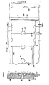
- the foundation for the assembly of LEDs is an aluminum alloy mother plate 10 which can be fastened into a printer.
- the front face of the mother plate has a peripheral groove 11 which receives the edge of a cover (not shown) which supports a lens for focusing the image of the LEDs onto a photo-receptor drum or the like.
- Near each end of the mother plate there are conventional electrical connectors 12 for bringing signals and power into the assembly.
- the mother plate serves as a ground plane for the LEDs and integrated circuits mounted in the assembly.
- the tiles are secured to the front face of the mother plate by an electrically condutive silver-filled epoxy adhesive and a quick setting acrylic adhesive.
- the electrically and thermally conductive adhesive is applied between a pair of parallel grooves 14 extending along the length of the plate.
- the acrylic adhesive is applied along the length of the plate between the lateral edge areas of the tiles and the mother plate outboard from the grooves 14. The grooves serve to isolate the two adhesives from each other.
- a row of LED dice 16 lies along the center of the assembly. Each die is about eight millimeters long and about a millimeter in width. Three such dice are cemented to the front face of each of the tiles by an electrically conductive silver-filled epoxy adhesive. On each side of the row of LED dice on each tile, there is a row of three integrated circuit chips 17. Electronic signal processing is conducted on the integrated circuit chips for supplying a current to selected light emitting diodes, as desired, during operation of the assembly. In an exemplary embodiment with 96 LEDs on each die, each chip has 48 integrated circuit LED current drivers for driving half of the LEDs on its respective die.
- the LEDs are precisely located on the dice by reason of the dice being carefully cut after the LEDs are fabricated.
- the LED dice are then accurately positioned on the tiles.
- the tiles are accurately positioned on the mother plate.
- the LEDs are precisely positioned on the mother plate.
- An exposed area 19 is left along each of the opposite lateral edges of each tile extending beyond the edge of the printed circuit board secured on the front face of the tile.
- These exposed areas on the front faces of the tiles are reference surfaces which are located in a reference plane by positioning them on a precision assembly fixture.
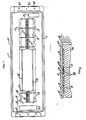
- FIGS. 2 and 3 illustrate, in fragmentary face view and cross-section, a fixture for assembling the dice on a tile.
- the fixture has a smooth, flat base plate 21 on which a mounting tile 13 is placed.
- the tile slides under a cantilevered overhang 22 on an dice reference guide 23.
- the tile is placed on the base plate with its front face up and with one edge (defined as the reference edge) abutting a shoulder 24 under the overhang.
- An undercut 26 in the dice reference guide causes the shoulder 24 to about just the front half of the reference edge of the tile.
- the tiles are not precisely rectangular. It is desirable to have an almost unnoticeable chamfer on each side of the tile extending from the locus of the LED dice near the center of the tile toward each lateral edge. A chamfer of as little as 1° has been found appropriate.
- a small flat 36 (not separately shown in the drawings) is left in the middle of the tile to serve as a reference point.
- the tapers make manufacturing easier.
- the critical dimension is the length of the LED array in the center portion of the tile. Thus, it is not necessary to maintain tight tolerances along the entire length of the tiles, but only in the area of the reference points or flats 36.
- One corner 28 of the tile on the opposite end from the reference surface is chamfered as a clear marker for proper orientation of the tile on the subassembly fixture, and later on the assembly fixture.
- the tile is alos placed in the assembly fixture so that the reference flat 36 on one side engages the edge of a side guide 27.
- the side guide is at precisely a right angle to the shoulder 24 on the dice reference guide which is in turn exactly parallel with the lip 25 on the overhang.
- the distance between the lip 25 and shoulder 24 is also precisely known. All of this assures that the tile is in a precisely known location with the reference edge of the tile abutted against the shoulder 24 throughout its length, and the center portion 36 of the side of the tile touching the side guide 27.
- the tile When the tile is in its proper location in the subassembly fixture, it can be temporarily held in place by a vacuum chuck (not shown) which simply applies a vacuum to the bottom face of the tile so that air pressure tightly holds it down.
- a vacuum chuck (not shown) which simply applies a vacuum to the bottom face of the tile so that air pressure tightly holds it down.
- a die 16 with a row of LEDs is placed with one edge against the lip 25 of the overhang and with an end against the side guide 27. This positions the die precisely with respect to the reference edge and one side of the tile.
- a second die is then placed with its edge against the lip of the overhang and its end abutting the end of the first die.
- a third die (not shown in FIG. 2) is then placed in an analogous location with an edge against the lip and its end against the end of the second die.
- the lip 25 aligns the three dice in a straight line parallel to and a known distance from the reference edge of the tile abutting the shoulder 24.
- the LED dice are themselves made with precision.
- the LEDs are formed by conventional techniques on arrays of putative dice on relatively large wafers. After testing to reject defective areas on a wafer, the wafer is scribed and broken, or precision sawed, or both, to produce the individual dice.
- the saw and scribe lines are located precisely with respect to the line of LEDs on the die to be formed so that the LEDs are in known locations on the dice.
- three thin pads of conductive epoxy adhesive are screen printed on the front face of the tile at the location where the dice are to be placed. As the dice are placed, they are moved at least a small distance laterally for assuring that the bottom surfaces are covered with adhesive and are pressed downwardly toward the tile for minimizing the thickness of adhesive between the dice and tile.
- the adhesive layer is of substantially uniform thickness and its rheological properties are such that slight pressure on the die assures tight seating and a substantially uniform thickness of adhesive between the dice and tile.
- the adhesive also serves to hold the dice in place on the tile when it is removed from the subassembly fixture for heat curing of the epoxy.
- An epoxy with high green strength assures the desired performance. It is also desirable that the adhesive, upon curing, leave a small gap between adjacent dice so that there is accommodation for the higher thermal expansion coefficient of the tiles than the coefficient of the GaAs of the LED dice.
- a suitable epoxy comprises Amicon C-850-5A available from the Polymer Products Division of Amicon Corporation, Lexington, Massachusetts.
- connection wires can be bonded between the LED dice and IC chips, and between the chips and PC boards in a conventional manner.
- the tile subassembly can be thoroughly tested. Typically, this involves testing the LEDs at a power level greater than expected in service to "burn in” the assembly. After “burn in” the tile can be tested for LED light output at a selected current, and the like. Testing at the subassembly stage can avoid loss of yield at the final assembly stage.
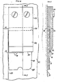
- Final assembly is conducted on an assembly fixture as illustrated in a fragmentary face view and cross-section in FIGS. 4 and 5.
- a plurality of tiles 13 are assembled front face down on a broad U-shaped z-base 31.
- the z-base has a raised rail 32 extending along each edge.
- the tops of the rails are ground precisely flat and smooth to serve as a reference plane for fixing the z position of the front faces of the tiles.
- the tiles are placed with the exposed areas 19 at each lateral edge resting atop the rails.
- the open channel of the4 z-base between the rails provides clearance for the PC boards 18, IC chips 17 and LED dice 16 on the front face of the tile, as can be best seen in FIG. 5.
- a row of holes 33 extend through the bottom of the z-base to permit viewing by a microscope (not shown) below the base. The holes are arranged so that the field of view includes the two sides of adjacent tiles.
- a first mounting tile is set on the fixture with one lateral edge against an edge guide 34 extending parallel to the rails.
- the same reference edge of the tile that was against the shoulder 24 (FIGS. 2 and 3) of the subassembly fixture is placed against the edge guide 34 of the assembly fixture.
- the edge guide 34 extends above the rails only the half thickness of the tiles so that it bears against the same part of the tile as the shoulder 24 on the subassembly fixture.
- the side of the first tile is located with the reference flat 36 in contact with a shoulder 35 perpendicular to the rails at the end of the fixture.
- a movable clamp 37 which bears against the lateral edge of the tile.
- Any of a variety of clamping mechanisms can be employed, including spring loading, a pneumatic actuator, solenoid, screw adjust, or the like.
- a second tile is placed front face down on the rails with its lateral edge tight against the edge guide 34.
- the space between the LEDs on the end dice on adjacent tiles is viewed with a microscope (which is conveniently connected to a video display for ease of viewing), and the second tile moved until the appropriate spacing is obtained.
- the second tile is then clamped in place. This process if repeated for each successive tile to assemble the full array of nine tiles (twenty-seven dice).
- a small space between the end dice on adjacent tiles is desirable to accommodate the greater thermal expansion of the aluminum mother plate than the stainless steel tiles.
- the assembly can again be checked for proper spacing before the tiles are finally locked in position.
- each end of the assembly fixture there is a surface 38 exactly coplanar with the tops of the rails 32. At least one, and as many as three, pins 39 protrude above that surface. Alternatively, the end surfaces 38 may be at a different, known elevation from the tops of the rails, or may be made adjustable for obtaining a desired Z dimension for the array of LEDs.
- a reference tile 41 (FIG. 1) is placed on that surface and located by the pins, which engage holes 40 in the reference tiles.
- the reference tiles can be positioned by one pin and a shoulder for engaging an edge of the tile 41.
- Each of the reference tiles has the same thickness as the tile on which the LED dice are located.
- the pins provide x and y locations which can later be used as references for lenses, mounting fixtures and the like.
- the mother plate is placed on top of the tiles and adhesively bonded thereto.
- Two types of adhesive are applied to the front face of the mother plate as mentioned hereinabove.
- An acrylic resin adhesive is applied on the front face of the mother plate outboard of the isolation grooves 14.
- An accelerator for the acrylic is applied on the corresponding areas on the backs of the tiles.
- a silver filled epoxy resin is applied on the mother plate between the grooves.
- the somewhat fluid adhesive accommodates variations in elevation of the backs of the tiles and surface flatness imperfections in the tiles by filling any gaps between the tiles and mother plate.
- the goal is to keep the LED top surfaces flat across the length of the array while keeping the manufacturing cost of the parts as low as possible. This is accomplished by taking up the tolerances in the variable thickness of adhesive between the mother plate and daughter tiles.
- the filling of the space between the tiles and mother plate is alos important to assure good thermal and electrical conductivity to the mother plate which serves as a heat sink and a ground plane.
- the accelerator and acrylic adhesive react to obtain a fast cure of the adhesive at room temperature. This permits the assembly to be removed from the fixture within a matter of a minute or so. The assembly is then heated to the curing temperature of the conductive epoxy as the final stage of mechanical assembly.
- the mounting tiles are made of stainless steel which receives thin electroless nickel plating and gold plating for preventing oxidation films that would increase electrical contact resistance. Resistance variations are to be avoided since these may affect the light output from the LEDs.
- Stainless steel is employed as a substrate since it has a coefficient of thermal expansion sufficiently close to the coefficient of expansion of the gallium arsenide LED dice and silicon integrated circuit chips to avoid breakage of these brittle components during low temperature excursions. Differences in coefficient of expansion are accommodated in the adhesive.
- the mother plate is preferably made of aluminum alloy for lighter weight and better thermal and electrical conductivity. Differences in coefficient of expansion between the aluminum and stainless steel can be accommodated by the adhesives.
- the holes 40 in the reference tiles at the ends of the assembly provide guidance for aligning the print head in a printer.
- the holes may be used as references for locating the x and y positions of the print head assembly. Since the front faces of the reference tiles are in precisely the same plane as the tiles on which the LED dice are positioned, the elevation or z position of a focussing lens for the LEDs, and of the print head in the printer can also be set. Either of these alignment or installation references may be complemented with additional adjustment features external to the print head assembly, if desired.
- the assembly fixture may be as illustrated in fragmentary transverse cross section in FIG. 6.
- This subassembly fixture comprises a base 46 having a recessed area having a raised reference face 47 at each end.
- the recessed area is subdivided into five shallow pockets by low walls 48.
- the two outer larger pockets accommodate printed circuit boards 18.
- two pockets accommodate rows of integrated circuit chips 17.
- the depth of the small pocket which accommodates the LED dice is precisely controlled so as to be a known distance below the reference plane formed by the two reference faces 47. This assures that the front face of the dice are a known distance above the front face of a tile.
- the depth of the other pockets is also controlled but need not be made to the same tolerance since the height of the IC chips and PC boards above the front face of the tile is not as critical.
- a row of LED dice are placed in the central pocket, front face down. One edge of each die is placed against one side wall of the pocket (to the right of FIG. 6). The end of the first LED die is pressed against one end of the pocket and the ends of the additional dice are abutted against the ends of the preceding dice.
- the integrated circuit chips are assembled in the fixture in the same manner, again abutting the side of each chip against an internal wall 48.
- the PC boards are similarly positioned in their respective pockets in the fixture.
- a tile 13 receives a screen printed pattern of adhesive on its front face corresponding to the pattern of components to be mounted on the tile.
- This adhesive coated tile is then placed on top of the upside-down components in the subassembly fixture for adhesive bonding.
- the reference lateral edge of the tile is abutted against an edge reference guide 49, thus assuring that all of the components mounted on the tile are correctly positioned.
- the adhesive between the tile and components accommodates variations in height of the components in the assembly fixture. If desired, the LED dice and integrated circuit chips may be assembled on a tile in such a fixture for precise positioning and the printed circuit boards later added in a separate operation.
- linear fixtures have been described and illustrated herein in the form of straight edges against which tiles, dice, or the like are placed. It will be recognized that it is not necessary to have a continuous straight edge to form a linear fixture and in fact only two points are required to form a linear fixture. Such a two point fixture is more susceptible to damage than a straight edge as described and is therefore less preferred. It will also be apparent that the planar fixtures may be interrupted with grooves or the like, much in the same way the rails on the assembly fixture are spaced apart from each other.
- Interrupted planar fixtures such as the rails are useful in an embodiment where the tiles have areas on the front which are to be placed against the planar fixture, and which do not extend the complete length of each lateral edge.
- reference areas may be left on the front of the tile near each corner, with a printed circuit board extending closer to the edge in a mid portion.
- conductive adhesive is used between the tiles and the LED dice and between the tiles and the mother plate so that the latter serves as a ground plane. Electrically insulating adhesive may be used with the ground made through the printed circuit board.
Landscapes
- Physics & Mathematics (AREA)
- Optics & Photonics (AREA)
- Health & Medical Sciences (AREA)
- General Health & Medical Sciences (AREA)
- Toxicology (AREA)
- Printers Or Recording Devices Using Electromagnetic And Radiation Means (AREA)
- Led Device Packages (AREA)
- Led Devices (AREA)
- Dot-Matrix Printers And Others (AREA)
Applications Claiming Priority (2)
| Application Number | Priority Date | Filing Date | Title |
|---|---|---|---|
| US07/256,001 US4942405A (en) | 1988-10-11 | 1988-10-11 | Light emitting diode print head assembly |
| US256001 | 1988-10-11 |
Publications (2)
| Publication Number | Publication Date |
|---|---|
| EP0364077A2 true EP0364077A2 (de) | 1990-04-18 |
| EP0364077A3 EP0364077A3 (de) | 1990-09-19 |
Family
ID=22970723
Family Applications (1)
| Application Number | Title | Priority Date | Filing Date |
|---|---|---|---|
| EP19890307837 Withdrawn EP0364077A3 (de) | 1988-10-11 | 1989-08-02 | Aufbau eines Druckkopfes mit Leuchtdioden |
Country Status (3)
| Country | Link |
|---|---|
| US (1) | US4942405A (de) |
| EP (1) | EP0364077A3 (de) |
| JP (1) | JPH02155671A (de) |
Cited By (2)
| Publication number | Priority date | Publication date | Assignee | Title |
|---|---|---|---|---|
| EP0781660A1 (de) * | 1995-12-26 | 1997-07-02 | Oki Electric Industry Co., Ltd. | Ausrichtung einer Leuchtdiodenanordnung |
| EP0960738A3 (de) * | 1998-05-29 | 2000-03-22 | Canon Kabushiki Kaisha | Halbleiterchipsteuerungsgerät und -steuerungsverfahren und Bildaufzeichnungsgerät und dessen Steuerungsverfahren |
Families Citing this family (18)
| Publication number | Priority date | Publication date | Assignee | Title |
|---|---|---|---|---|
| US5177502A (en) * | 1988-03-15 | 1993-01-05 | Siemens Aktiengesellschaft | Arrangement for detachably fastening modules to a module carrier |
| JPH03153372A (ja) * | 1989-10-26 | 1991-07-01 | Hewlett Packard Co <Hp> | 発光ダイオード・プリントヘッド |
| US5317344A (en) * | 1989-12-22 | 1994-05-31 | Eastman Kodak Company | Light emitting diode printhead having improved signal distribution apparatus |
| US5250963A (en) * | 1989-12-27 | 1993-10-05 | Am International, Inc. | Imaging diode array and system |
| EP0464269B1 (de) * | 1990-07-03 | 1995-11-02 | Agfa-Gevaert N.V. | Led-Belichtungskopf |
| US5257049A (en) * | 1990-07-03 | 1993-10-26 | Agfa-Gevaert N.V. | LED exposure head with overlapping electric circuits |
| US5084714A (en) * | 1990-11-28 | 1992-01-28 | Eastman Kodak Company | Narrow led printheads and gradient index lens array for use therewith |
| US5453145A (en) * | 1991-03-04 | 1995-09-26 | Eastman Kodak Company | Z-axis dimensional control in manufacturing an LED printhead |
| US5606358A (en) * | 1991-12-23 | 1997-02-25 | Eastman Kodak Company | Light-emitting diode printhead |
| US5442388A (en) * | 1992-01-16 | 1995-08-15 | Xerox Corporation | Method and means for correcting lateral registration errors |
| US5646674A (en) * | 1994-04-29 | 1997-07-08 | Eastman Kodak Company | Optical print head with flexure mounted optical device |
| US6057871A (en) * | 1998-07-10 | 2000-05-02 | Litton Systems, Inc. | Laser marking system and associated microlaser apparatus |
| AU2006203379B2 (en) * | 2000-10-20 | 2008-02-28 | Memjet Technology Limited | A Modular Printhead Assembly Incorporating a Plurality of Complementary Printhead Modules |
| US20060082297A1 (en) * | 2004-10-19 | 2006-04-20 | Eastman Kodak Company | Method of preparing a lens-less LED |
| DE102008005345A1 (de) | 2007-09-28 | 2009-04-02 | Osram Opto Semiconductors Gmbh | Halbleiterbasiertes Bauelement, Aufnahme für ein halbleiterbasiertes Bauelement und Verfahren zur Herstellung eines halbleiterbasierten Bauelements |
| EP2218571A1 (de) | 2009-01-30 | 2010-08-18 | Nederlandse Organisatie voor toegepast -natuurwetenschappelijk onderzoek TNO | Beleuchtungssystem zur Verwendung in einer Stereolithographievorrichtung |
| US9180684B2 (en) * | 2013-12-18 | 2015-11-10 | Xerox Corporation | Autofocus LED print head mechanism |
| US9599723B2 (en) | 2015-08-18 | 2017-03-21 | Carestream Health, Inc. | Method and apparatus with tiled image sensors |
Family Cites Families (8)
| Publication number | Priority date | Publication date | Assignee | Title |
|---|---|---|---|---|
| US3952311A (en) * | 1972-04-24 | 1976-04-20 | The Laitram Corporation | Electro-optical printing system |
| GB2099221B (en) * | 1981-05-26 | 1985-11-20 | Purdy Haydn Victor | Light emitting diode array devices and image transfer systems |
| EP0086907B1 (de) * | 1982-02-19 | 1987-05-06 | Agfa-Gevaert N.V. | Aufzeichnungsapparat |
| EP0115088B1 (de) * | 1983-01-21 | 1986-12-30 | Agfa-Gevaert N.V. | Aufzeichnungsgerät |
| US4566170A (en) * | 1983-05-10 | 1986-01-28 | Pitney Bowes Inc. | Method of producing a light emiting diode array |
| JPS6129562A (ja) * | 1984-07-20 | 1986-02-10 | Sanyo Electric Co Ltd | 印字用発光ダイオ−ド |
| US4605944A (en) * | 1984-09-11 | 1986-08-12 | Sanyo Electric Co., Ltd. | LED array device for printer |
| JPH0647300B2 (ja) * | 1984-12-13 | 1994-06-22 | 三洋電機株式会社 | 像形成装置 |
-
1988
- 1988-10-11 US US07/256,001 patent/US4942405A/en not_active Expired - Fee Related
-
1989
- 1989-08-02 EP EP19890307837 patent/EP0364077A3/de not_active Withdrawn
- 1989-10-11 JP JP1264816A patent/JPH02155671A/ja active Pending
Cited By (5)
| Publication number | Priority date | Publication date | Assignee | Title |
|---|---|---|---|---|
| EP0781660A1 (de) * | 1995-12-26 | 1997-07-02 | Oki Electric Industry Co., Ltd. | Ausrichtung einer Leuchtdiodenanordnung |
| US5943586A (en) * | 1995-12-26 | 1999-08-24 | Oki Electric Industry Co., Ltd. | LED array alignment mark, method and mask for forming same, and LED array alignment method |
| US6023104A (en) * | 1995-12-26 | 2000-02-08 | Oki Electric Industry Co., Ltd. | LED array alignment mark, method and mask for forming same, and LED array alignment method |
| EP0960738A3 (de) * | 1998-05-29 | 2000-03-22 | Canon Kabushiki Kaisha | Halbleiterchipsteuerungsgerät und -steuerungsverfahren und Bildaufzeichnungsgerät und dessen Steuerungsverfahren |
| US6624838B2 (en) | 1998-05-29 | 2003-09-23 | Canon Kabushiki Kaisha | Semiconductor-chip control apparatus and control method and image recording apparatus and its control method |
Also Published As
| Publication number | Publication date |
|---|---|
| US4942405A (en) | 1990-07-17 |
| EP0364077A3 (de) | 1990-09-19 |
| JPH02155671A (ja) | 1990-06-14 |
Similar Documents
| Publication | Publication Date | Title |
|---|---|---|
| US4942405A (en) | Light emitting diode print head assembly | |
| US5014074A (en) | Light emitting diode print head assembly | |
| US5617131A (en) | Image device having a spacer with image arrays disposed in holes thereof | |
| EP0736900B1 (de) | Ersetzung von Halbleiterchips in einer Matrix von ganzer Breite | |
| EP2391498B1 (de) | Beleuchtungssystem zur verwendung in einer stereolithographievorrichtung | |
| US5134340A (en) | Light-emitting diode printhead | |
| US4999077A (en) | Method of fabricating full width scanning or imaging arrays from subunits | |
| EP0454167A2 (de) | Aus Schichten aufgebauter elektrostatischer Druckkopf | |
| US6831673B2 (en) | Optical write head, and method of assembling the same | |
| US7880190B2 (en) | Combined semiconductor device, LED print head, and image forming apparatus | |
| US5173759A (en) | Array of light emitting devices or photo detectors with marker regions | |
| US4851862A (en) | Led array printhead with tab bonded wiring | |
| US6020750A (en) | Wafer test and burn-in platform using ceramic tile supports | |
| CA1236908A (en) | Light emitting diode array and method of producing the same | |
| US4899174A (en) | Method of making LED array printhead with tab bonded wiring | |
| US5079567A (en) | Leaf-spring assembly for LED printhead | |
| US5870128A (en) | Light-emitting device assembly having in-line light-emitting device arrays and manufacturing method therefor | |
| US5453145A (en) | Z-axis dimensional control in manufacturing an LED printhead | |
| EP0510274A1 (de) | Leuchtdiodendruckkopf | |
| GB2226185A (en) | A light emitting apparatus | |
| CN120601241A (zh) | 一种超大阵列多芯片封装结构、多芯片封装工艺及其检测方法 | |
| JPH06112526A (ja) | 半導体チップアレイ及びそのための半導体チップの形成パターン及びそのダイシング方法 | |
| JPS63205950A (ja) | イメ−ジセンサのチツプ固定方法 | |
| JPH07177304A (ja) | 画像装置 | |
| JPH10129036A (ja) | 光プリンタヘッド |
Legal Events
| Date | Code | Title | Description |
|---|---|---|---|
| PUAI | Public reference made under article 153(3) epc to a published international application that has entered the european phase |
Free format text: ORIGINAL CODE: 0009012 |
|
| AK | Designated contracting states |
Kind code of ref document: A2 Designated state(s): BE DE FR GB |
|
| PUAL | Search report despatched |
Free format text: ORIGINAL CODE: 0009013 |
|
| RHK1 | Main classification (correction) |
Ipc: H04N 1/036 |
|
| AK | Designated contracting states |
Kind code of ref document: A3 Designated state(s): BE DE FR GB |
|
| 17P | Request for examination filed |
Effective date: 19910225 |
|
| 17Q | First examination report despatched |
Effective date: 19930317 |
|
| STAA | Information on the status of an ep patent application or granted ep patent |
Free format text: STATUS: THE APPLICATION IS DEEMED TO BE WITHDRAWN |
|
| 18D | Application deemed to be withdrawn |
Effective date: 19930928 |