EP0364095A2 - Procédé de post-termination pour des résistances à film épais de panneaux à circuit imprimé - Google Patents
Procédé de post-termination pour des résistances à film épais de panneaux à circuit imprimé Download PDFInfo
- Publication number
- EP0364095A2 EP0364095A2 EP89308931A EP89308931A EP0364095A2 EP 0364095 A2 EP0364095 A2 EP 0364095A2 EP 89308931 A EP89308931 A EP 89308931A EP 89308931 A EP89308931 A EP 89308931A EP 0364095 A2 EP0364095 A2 EP 0364095A2
- Authority
- EP
- European Patent Office
- Prior art keywords
- layer
- composition
- thick film
- printed circuit
- resistors
- Prior art date
- Legal status (The legal status is an assumption and is not a legal conclusion. Google has not performed a legal analysis and makes no representation as to the accuracy of the status listed.)
- Withdrawn
Links
Images


Classifications
-
- H—ELECTRICITY
- H05—ELECTRIC TECHNIQUES NOT OTHERWISE PROVIDED FOR
- H05K—PRINTED CIRCUITS; CASINGS OR CONSTRUCTIONAL DETAILS OF ELECTRIC APPARATUS; MANUFACTURE OF ASSEMBLAGES OF ELECTRICAL COMPONENTS
- H05K1/00—Printed circuits
- H05K1/16—Printed circuits incorporating printed electric components, e.g. printed resistors, capacitors or inductors
- H05K1/167—Printed circuits incorporating printed electric components, e.g. printed resistors, capacitors or inductors incorporating printed resistors
-
- H—ELECTRICITY
- H01—ELECTRIC ELEMENTS
- H01C—RESISTORS
- H01C1/00—Details
- H01C1/14—Terminals or tapping points specially adapted for resistors; Arrangements of terminals or tapping points on resistors
- H01C1/142—Terminals or tapping points specially adapted for resistors; Arrangements of terminals or tapping points on resistors the terminals or tapping points being coated on the resistive element
-
- H—ELECTRICITY
- H01—ELECTRIC ELEMENTS
- H01C—RESISTORS
- H01C17/00—Apparatus or processes specially adapted for manufacturing resistors
- H01C17/28—Apparatus or processes specially adapted for manufacturing resistors adapted for applying terminals
- H01C17/281—Apparatus or processes specially adapted for manufacturing resistors adapted for applying terminals by thick film techniques
-
- H—ELECTRICITY
- H01—ELECTRIC ELEMENTS
- H01C—RESISTORS
- H01C7/00—Non-adjustable resistors formed as one or more layers or coatings; Non-adjustable resistors made from powdered conducting material or powdered semi-conducting material with or without insulating material
- H01C7/003—Thick film resistors
-
- H—ELECTRICITY
- H05—ELECTRIC TECHNIQUES NOT OTHERWISE PROVIDED FOR
- H05K—PRINTED CIRCUITS; CASINGS OR CONSTRUCTIONAL DETAILS OF ELECTRIC APPARATUS; MANUFACTURE OF ASSEMBLAGES OF ELECTRICAL COMPONENTS
- H05K1/00—Printed circuits
- H05K1/02—Details
- H05K1/03—Use of materials for the substrate
- H05K1/0306—Inorganic insulating substrates, e.g. ceramic, glass
-
- H—ELECTRICITY
- H05—ELECTRIC TECHNIQUES NOT OTHERWISE PROVIDED FOR
- H05K—PRINTED CIRCUITS; CASINGS OR CONSTRUCTIONAL DETAILS OF ELECTRIC APPARATUS; MANUFACTURE OF ASSEMBLAGES OF ELECTRICAL COMPONENTS
- H05K1/00—Printed circuits
- H05K1/02—Details
- H05K1/09—Use of materials for the conductive, e.g. metallic pattern
- H05K1/092—Dispersed materials, e.g. conductive pastes or inks
-
- H—ELECTRICITY
- H05—ELECTRIC TECHNIQUES NOT OTHERWISE PROVIDED FOR
- H05K—PRINTED CIRCUITS; CASINGS OR CONSTRUCTIONAL DETAILS OF ELECTRIC APPARATUS; MANUFACTURE OF ASSEMBLAGES OF ELECTRICAL COMPONENTS
- H05K2201/00—Indexing scheme relating to printed circuits covered by H05K1/00
- H05K2201/03—Conductive materials
- H05K2201/0332—Structure of the conductor
- H05K2201/0335—Layered conductors or foils
- H05K2201/035—Paste overlayer, i.e. conductive paste or solder paste over conductive layer
-
- H—ELECTRICITY
- H05—ELECTRIC TECHNIQUES NOT OTHERWISE PROVIDED FOR
- H05K—PRINTED CIRCUITS; CASINGS OR CONSTRUCTIONAL DETAILS OF ELECTRIC APPARATUS; MANUFACTURE OF ASSEMBLAGES OF ELECTRICAL COMPONENTS
- H05K2201/00—Indexing scheme relating to printed circuits covered by H05K1/00
- H05K2201/03—Conductive materials
- H05K2201/0332—Structure of the conductor
- H05K2201/0388—Other aspects of conductors
- H05K2201/0391—Using different types of conductors
-
- H—ELECTRICITY
- H05—ELECTRIC TECHNIQUES NOT OTHERWISE PROVIDED FOR
- H05K—PRINTED CIRCUITS; CASINGS OR CONSTRUCTIONAL DETAILS OF ELECTRIC APPARATUS; MANUFACTURE OF ASSEMBLAGES OF ELECTRICAL COMPONENTS
- H05K2203/00—Indexing scheme relating to apparatus or processes for manufacturing printed circuits covered by H05K3/00
- H05K2203/14—Related to the order of processing steps
- H05K2203/1453—Applying the circuit pattern before another process, e.g. before filling of vias with conductive paste, before making printed resistors
-
- H—ELECTRICITY
- H05—ELECTRIC TECHNIQUES NOT OTHERWISE PROVIDED FOR
- H05K—PRINTED CIRCUITS; CASINGS OR CONSTRUCTIONAL DETAILS OF ELECTRIC APPARATUS; MANUFACTURE OF ASSEMBLAGES OF ELECTRICAL COMPONENTS
- H05K2203/00—Indexing scheme relating to apparatus or processes for manufacturing printed circuits covered by H05K3/00
- H05K2203/14—Related to the order of processing steps
- H05K2203/1461—Applying or finishing the circuit pattern after another process, e.g. after filling of vias with conductive paste, after making printed resistors
Definitions
- This invention relates to printed circuits and in particular to printed circuits that include thick film resistors.
- Typical thick film resistors comprise a patterned layer (film) of a suitable resistive material of between 0.00508 and 0.0508 mm (0.2 and 2.0 mils) thick deposited on an insulating substrate.
- a thick film resistor is typically formed by first printing an appropriately patterned layer of suitably wet composition, usually an ink or paste, on an appropriate insulating substrate, generally an alumina ceramic board. Patterning is usually controlled by silk screen printing. The resistive composition is thereafter dried and fired (heated) to form the resistor.
- printed circuit boards employ a first composition of inks or pastes for forming high resistance resistors and a different second composition for forming lower-resistance resistors.
- the resistance R of a particular resistor composition is generally tailored by adjusting its aspect ratio, L/W, where L is the length and W the width of the resistive film. R increases directly with L and inversely with W. R also increases inversely with the thickness of the film, but the thickness is generally kept uniform to facilitate processing.
- the printed circuit board typically supports a number of circuit elements (components) that are interconnected into a desired electrical circuit by an appropriately configured conductive film that is printed on the circuit board in an analogous fashion.
- Copper (or a copper-rich alloy) is typically used on many printed circuit boards as the conductive film that interconnects the circuit elements since copper is of low cost, conducts well, resists migration and is easily soldered to.
- the copper film typically used is printed as a suspension of copper particles which is best fired in a nitrogen atmosphere to sinter the copper particles without oxidation into a good conductor. Materials typically preferred for forming thick film resistors are best fired in air.
- One problem is that copper films that have been formed by firing in nitrogen lose many of their favourable properties if subsequently re-fired in air.
- One proposed solution to this problem is to first fire the thick film resistors in air and then to add copper conductors to the ends of the thick film resistors so as to make electrical contacts thereto. The copper conductors are then fired in nitrogen.
- This technique in which the thick film resistors are formed first and their connections (terminations) are provided later, is generally known as "post-termination".
- post-termination A problem with this type of post-termination is that copper conductors generally make poor (high resistance) and non-uniform interfaces with the resistive film materials used in high performance thick film resistors, such as those based on a ruthenium compound (RuO2 or Bi2Ru2O7) for resistances above about 2,500 ohms.
- RuO2 or Bi2Ru2O7 ruthenium compound
- the invention provides an improved technique, particularly useful for post-termination, but not limited thereto, of high-resistance (e.g. about 2,500 ohms or larger) thick film resistors.
- high-resistance e.g. about 2,500 ohms or larger
- One embodiment of the invention is directed to a post-termination process in which a layer of a high-resistivity composition for example, 25,000 ohms per square sheet resistivity, is first deposited in a pattern suitable for forming the desired high-resistance resistors. Then a layer of a lower-resistivity composition, for example 100 ohms per square sheet resistivity, is deposited in a pattern that not only includes the desired low-resistance resistors, but also includes separate portions that overlap end portions of each of the high-resistance resistors deposited earlier. These separate portions of low-resistivity material serve as termination regions (electrical contact end areas) of the high-resistance resistors. Thereafter a common firing step is used to fire both the high-resistivity and low-resistivity compositions. To this end, the two compositions are chosen to be amenable to a common firing step.
- a high-resistivity composition for example, 25,000 ohm
- Another embodiment of the invention is directed to a post-termination process in which a low-resistivity composition is first deposited in a suitable pattern that includes not only the low-resistivity resistors but also portions suitable for termination regions.
- a high-resistivity composition is then deposited to define high-resistance resistors whose ends partially overlap the previously deposited portion of low-resistivity composition designed to serve as termination regions for such resistors.
- the two compositions are then fired, as before, in a common firing step.
- the copper interconnection film is deposited to overlap the termination regions both of the high-resistance and of the low-resistance resistors.
- Another embodiment of the invention is directed to a process in which the conductive film is deposited first, as is characteristic of standard terminations.
- the layer of low-resistivity composition is then deposited either before or after the layer of high-resistivity composition. It is made to contact both the conductive layer and the high-resistivity layer.
- the layer of low resistivity again serves as an interface between the conductive layer and the layer of high resistivity.
- the invention is directed to a printed circuit including at least one thick film resistor comprising a printed circuit board, a patterned layer of a first composition for providing at least one thick film resistor, termination means at each end of the resistor and a conductive layer for connecting to the resistor.
- the termination means includes a portion of a layer of a second composition whose resistivity is lower than the resistivity of the first composition.
- the layer portion of the second composition forms a first extended interface with each end of the resistor.
- the conductive layer in turn forms a second extended interface with the layer portion of the second composition of each of the termination means.
- the invention should be generally applicable to improving the terminations of thick film resistors formed of high-resistivity compositions where there is a strong dependence of sheet resistance on aspect ratio.
- the invention may be viewed as the inclusion, in a printed circuit that is subject to such dependence, of an appropriate interface film between each end of a thick film resistor and the conductive connection thereto.
- the composition of the interface film generally has a resistivity lower than that of the composition of the thick film resistor, advantageously by at least a factor of 10, and preferably by a factor of 100.
- Circuit board 10 includes a ceramic substrate 14 having a top surface 11 on which lies the layer 12 which is of relatively high-resistivity sheet material and which has end portions 12A and 12B, a layer 16 of lower-resistivity material having portions 16A and 16B, and a conductive layer 18 having portions 18A and 18B.
- the sheet resistivities of layers 12 and 16 are 25,000 and 100 ohms/square, respectively
- substrate 14 is alumina
- conductive layer 18 is copper or a copper-rich alloy.
- the break shown in about the centre of board 10 is used to denote that a body portion of the resistor of layer 12 is typically longer than the end portions 12A and 12B.
- the break shown in about the middle of the height of substrate 14 denotes that substrate 14 is typically considerably thicker than the layers deposited thereon.
- Layer 12 which is suitable for use in a high-resistance resistor, is first deposited on the substrate 14, typically as part of a larger layer consisting of many discrete portions suitable for forming many high value resistors.
- layer portions 16A and 16B which are useful as low-resistance contact regions, are also deposited on the substrate 14.
- Layer portions 16A and 16B typically also are parts of a larger layer consisting of several discrete portions of the low-resistivity material (e.g., 100 ohms/square) that also serves to provide several low-value resistors of the printed circuit. Portions 16A and 16B overlap the full widths of respective end portions 12A and 12B of the layer 12.
- the separate copper layer portions 18A and 18B of layer 18 are deposited on the top surface 11 of the substrate 14 and each overlaps the full width of an end portion of layer portions 16A and 16B, respectively.
- the layer portions 18A and 18B also are typically parts of a larger copper layer consisting of many discrete portions used to interconnect various other circuit elements on the printed circuit board 10.
- the lengths of the overlaps while not critical, are adequate to ensure that the layer portions 16A and 16B have low-resistance interfaces with both layer portions 12A and 12B respectively, and with layer portions 18A and 18B, respectively.
- the resistances of such extended interfaces preferably are typically a small fraction, generally no more than a few percent, of the total resistance to be provided by the thick film resistor.
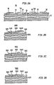
- FIG. 1B there is shown a portion of a printed circuit 101B including a ceramic substrate 141B. This supports a high-resistivity layer portion 12A1B, a low-resistivity layer portion 16A1B, and a conductive layer portion 18A1B, corresponding to portions 12A, 16A, and 18A of the printed circuit 10 shown in Figure 1A. As seen in this embodiment, the conductive layer portion 18A1B extends over the full length of low-resistivity layer 16A1B.
- ceramic substrate 141C supports high-resistivity layer portions 12A1C, low-resistivity layer portions 16A1C and conductive layer portions 18A1C.
- the conductive layer portion 18A1C overlaps only a part of low-resistivity layer portion 16A1C that overlies the high resistivity layer portion 12A1C.
- Figure 1D there is shown an embodiment in which the conductive layer portion 18A1D overlies only a portion of a low-resistivity layer 16A1D that lies directly on ceramic substrate top surface 111D and does not overlap the portion that overlies the high-resistivity layer portion 12A1D.
- compositions used for high performance thick film resistors generally are mixtures of particles of a ruthenium compound, such as RuO2 or Bi2Ru2O7, particles of a lead borosilicate glass, traces of Temperature Coefficient of Resistance (TCR) modifiers and a screening agent.
- the screening agent is typically an organic vehicle that includes a solvent and a resin. It is used both to keep the particles in suspension and to provide good flow properties to facilitate deposition by screen printing.
- These compositions are commercially available from DuPont Electronics, U.S.A. as the 1600 Birox series of resistors.
- the low-resistivity layer 16 uses a 100 ohm per square composition which DuPont denotes by the product number of 1621.
- Such a composition typically includes between 15 and 20 per cent ruthenium compound and 55 to 60 percent glass and is fired in conventional fashion as prescribed by the supplier using an 850 degree C peak temperature.
- the 25,000 ohm per square composition is formed by blending DuPont product numbers 1641 (10,000 ohm per square) and 1651 material (100,000 ohm per square).
- Such a blend typically includes between 5 and 10 percent ruthenium compound and 65 to 70 percent glass. It too is fired in the prescribed fashion set forth above.
- the different members of the series differ in the relative proportions of the ruthenium compound and the glass included, the more glass the higher the resistivity. Because higher-resistivity films have higher glass content, they form a more glassy surface that has a higher resistance to electrical contact thereto. This higher resistance becomes especially significant when the interface is a copper film and among other disadvantages results in a strong dependence of sheet resistance on the aspect ratio of the resistor. It has been found that these disadvantages are lessened significantly when a region of low-resistivity material is interposed between the high-resistance film and the copper film.
- the copper layer preferably used is a special copper thick film composition commercially available from DuPont Electronics, U.S.A. as DuPont 6001. It comprises finely divided copper particles, a screening agent and small amounts of additives to promote sintering and adhesion. After firing in nitrogen, as prescribed by the supplier with a peak temperature of 600 degrees C, the layer is about ninety-five per cent copper. Other compositions should be feasible, including some that include one or more other metals that alloy with copper to provide special properties.
- a thickness of about 0.0127 mm (0.5 mil) is common for thick film resistors although thicker and thinner layers are feasible.
- both the width and length of thick film resistors are generally between 0.508 and 5.08 mm (20 and 200 mils) and the aspect ratio tends to be between 0.1 and 10.0, the most widely used range being 0.2 to 5.0.
- compositions above described that it is advantageous to provide at least 0.127 mm (5 mils) of overlapping along the length of both for the termination regions and for the copper interfaces. This amount of overlap is usually enough to ensure the desired low resistance of the interface and also to facilitate satisfactory registration in printing.
- the termination regions that are included in the low-resistance resistors are made wider than the high-resistivity layers and narrower than the copper layers to which they interface. This is best seen in the top view of Figure 5 which will be described more fully below.
- the copper layer is made wider than the low-resistivity layers.
- Printed circuit board 50 comprises an insulator substrate 52 having a top surface 64 on which lies separate termination regions 56 and 58, a resistor 54 having end portions 54A and 54B overlapping the termination regions 56 and 58, respectively, and separate conductors 60 and 62 overlapping termination regions 56 and 58, respectively.
- the break shown in about the centre of board 50 is used to denote that a body portion of the resistor 54 is typically longer than the end portions 54A and 54B.
- the substrate 52 is typically considerably thicker than the layers deposited thereon.
- a layer of low-resistivity composition is deposited over the top surface 64 of substrate 52 to form separate regions 56 and 58 that serve as low-resistance electrical contacts to end portions 54A and 54B respectively, of resistor 54. This layer is also used to form the desired number of low-value resistors (not shown) on the printed circuit board 50.
- a layer of high-resistivity composition is deposited over the top surface 64 of substrate 52 to form resistor 54. This layer is dimensioned such that resistor 54 has the desired resistance. End portions 54A and 54B of the resistor 54 overlap portions of termination regions 56 and 58, respectively.
- the amount of overlap 0.127 mm (about (5 mils) in a typical embodiment) is sufficient to ensure that the interface resistance is at an acceptably small value.
- regions 56 and 58 and resistor 54 are fired in a common firing step.
- a conductive copper-rich layer is deposited over the top surface 64 of substrate 52. This layer includes portions 60 and 62 that overlap and make low-resistance electrical contacts to regions 56 and 58, respectively.
- the amount of overlap, as discussed above, is typically about 0.127 mm (5 mils).
- the conductive layer 602B is shown extending fully over the low-resistivity layer 562B including the portion underlying the high-resistivity layer 54A2B.
- the conductive layer 602C only partially overlies the portion of low-resistivity layer 562C that underlies the high-resistivity layer 54A2C.
- the conductive layer 602D extends over only a portion of low-resistivity layer 562D and avoids overlapping the high-resistivity layer portion 54A2D.
- a printed circuit board 69 in which a conductive layer 70 is first deposited over a ceramic substrate 72, as is characteristic of a standard termination. This is followed by the deposition of a low-resistivity layer 74, typically as part of a larger layer consisting of many discrete portions. As shown, layer 74 includes a portion 74A that overlaps the conductive layer 70 and a portion 74B that lies on the substrate 72. Then a layer 76 of high-resistivity composition is deposited to form a thick film resistor.
- the various factors previously discussed for the configuration, degree of overlap, and compositions of the various layers are generally applicable to this embodiment.
- a printed circuit board 79 in which a conductive layer 80 is first deposited over a ceramic substrate 82. This is followed by deposition of a high-resistivity layer 84 that forms a thick film resistor. Finally, a low-resistivity layer 86 is deposited to overlap both conductive layer 80 and the high-resistivity layer 84. Again, the factors previously discussed for the geometric degree of overlap, and compositions of the various layers are generally applicable here.
- the embodiments of Figures 3 and 4 can tolerate a wider range of compositions for the conductive layers than can the embodiments discussed earlier herein.
- the conductive layers can be of copper.
- the composition of the resistive layers should be compatible therewith.
- the conductive layer may be of copper fired in nitrogen at 900°C.
- the resistive layers are chosen so that they can be printed and fired in nitrogen at 900°C.
- the conductor can be of a noble metal or an alloy of noble metals, such as Ag, Au, Ag-Pd, that can be fired in air, for example, at 850°C.
- the resistive layers are chosen so that they can be printed and fired in air at 850°C.
- FIG. 5 there is shown a top view of a portion of a printed circuit 30 that includes a pair of low-resistance resistors 31 and 32, a high-resistance resistor 34 and a copper layer 36 that provides interconnections.
- the resistor 34 is provided with termination regions 34A and 34B, of any of the kinds described previously.
- the copper film 36 interconnects the resistors 31, 32 and 34 into a T section.
- the copper film 36 is deposited to include portions 36A that overlap the ends of the low resistance resistors 31 and 32 and portions 36B that overlap portions of the termination regions 34A and 34B serving as extended terminations for the high-resistance resistor 34.
- compositions providing a sheet resistivity of 100 ohms/square are used to form the low-resistance resistors (10 ohms to 1000 ohms) and compositions providing a sheet resistivity of 25,000 ohms/square are used to form the high-resistance resistors (2500 to 250,000 ohms).
- resistors of intermediate resistance 1000 to 2500 ohms
- a composition providing a sheet resistivity of 1750 ohms/square is appropriate for use in forming such resistors.
- the desirability of using a termination region of lower resistivity also increases.
- circuit elements such as capacitors, inductors, diodes and transistors on the printed circuit board in customary fashion.
- compositions for the thick film resistors It is, of course, feasible to use a variety of compositions for the thick film resistors. To the extent that such compositions result in resistors that profit by the inclusions of post-terminations in the manner discussed, the principles of this invention should be applicable.
- termination regions are portions of a layer of low-resistivity composition used only to provide such terminations.
Landscapes
- Engineering & Computer Science (AREA)
- Microelectronics & Electronic Packaging (AREA)
- Manufacturing & Machinery (AREA)
- Physics & Mathematics (AREA)
- Electromagnetism (AREA)
- Parts Printed On Printed Circuit Boards (AREA)
- Apparatuses And Processes For Manufacturing Resistors (AREA)
- Non-Adjustable Resistors (AREA)
Applications Claiming Priority (2)
| Application Number | Priority Date | Filing Date | Title |
|---|---|---|---|
| US256017 | 1988-10-11 | ||
| US07/256,017 US5169679A (en) | 1988-10-11 | 1988-10-11 | Post-termination apparatus and process for thick film resistors of printed circuit boards |
Publications (2)
| Publication Number | Publication Date |
|---|---|
| EP0364095A2 true EP0364095A2 (fr) | 1990-04-18 |
| EP0364095A3 EP0364095A3 (fr) | 1990-11-07 |
Family
ID=22970782
Family Applications (1)
| Application Number | Title | Priority Date | Filing Date |
|---|---|---|---|
| EP19890308931 Withdrawn EP0364095A3 (fr) | 1988-10-11 | 1989-09-04 | Procédé de post-termination pour des résistances à film épais de panneaux à circuit imprimé |
Country Status (4)
| Country | Link |
|---|---|
| US (2) | US5169679A (fr) |
| EP (1) | EP0364095A3 (fr) |
| JP (1) | JPH0724331B2 (fr) |
| KR (1) | KR920005985B1 (fr) |
Cited By (1)
| Publication number | Priority date | Publication date | Assignee | Title |
|---|---|---|---|---|
| EP1082882A4 (fr) * | 1999-03-17 | 2005-10-12 | Motorola Inc | Procede de fabrication de resistances |
Families Citing this family (11)
| Publication number | Priority date | Publication date | Assignee | Title |
|---|---|---|---|---|
| JPH05275958A (ja) * | 1992-03-25 | 1993-10-22 | Murata Mfg Co Ltd | ノイズフィルタ |
| US5952205A (en) | 1998-02-06 | 1999-09-14 | Neose Technologies, Inc. | Process for processing sucrose into glucose and fructose |
| GB9813668D0 (en) * | 1998-06-25 | 1998-08-26 | Sentec Ltd | Printed circuit board current sensor |
| US6510503B2 (en) | 1998-07-27 | 2003-01-21 | Mosaid Technologies Incorporated | High bandwidth memory interface |
| US5998177A (en) * | 1998-11-19 | 1999-12-07 | Neose Technologies, Inc. | Process for processing sucrose into glucose |
| JP4780689B2 (ja) * | 2001-03-09 | 2011-09-28 | ローム株式会社 | チップ抵抗器 |
| WO2003107361A1 (fr) * | 2002-06-13 | 2003-12-24 | ローム株式会社 | Resistance a puce presentant une faible resistance et son procede de production |
| US20040216303A1 (en) * | 2003-05-01 | 2004-11-04 | Berlin Carl W. | Thick film current sensing resistor and method |
| US7224258B2 (en) * | 2004-09-27 | 2007-05-29 | Ohmcraft, Inc. | Fine line thick film resistors by photolithography |
| US9700227B2 (en) | 2013-09-25 | 2017-07-11 | Bardy Diagnostics, Inc. | Ambulatory electrocardiography monitoring patch optimized for capturing low amplitude cardiac action potential propagation |
| US11723575B2 (en) | 2013-09-25 | 2023-08-15 | Bardy Diagnostics, Inc. | Electrocardiography patch |
Family Cites Families (28)
| Publication number | Priority date | Publication date | Assignee | Title |
|---|---|---|---|---|
| GB672255A (en) * | 1949-06-02 | 1952-05-21 | Ward Blenkinsop & Co Ltd | Improvements in the production of conducting layers upon electrical resistors |
| US3337832A (en) * | 1965-01-26 | 1967-08-22 | Sprague Electric Co | Resistor |
| US3717483A (en) * | 1969-04-22 | 1973-02-20 | Ibm | Metallizing composition |
| US3609105A (en) * | 1970-06-08 | 1971-09-28 | Alpha Metals | Metalizing material |
| US3679606A (en) * | 1970-09-08 | 1972-07-25 | Du Pont | Thermistor compositions and thermistors made therefrom |
| US3992212A (en) * | 1972-08-18 | 1976-11-16 | Universal Oil Products Company | Electrical resistor inks |
| US3914514A (en) * | 1973-08-16 | 1975-10-21 | Trw Inc | Termination for resistor and method of making the same |
| US4031272A (en) * | 1975-05-09 | 1977-06-21 | Bell Telephone Laboratories, Incorporated | Hybrid integrated circuit including thick film resistors and thin film conductors and technique for fabrication thereof |
| US4063993A (en) * | 1975-07-07 | 1977-12-20 | National Semiconductor Corporation | Method of making gang bonding interconnect tape for semiconductive devices |
| JPS5513922U (fr) * | 1978-07-08 | 1980-01-29 | ||
| US4331740A (en) * | 1980-04-14 | 1982-05-25 | National Semiconductor Corporation | Gang bonding interconnect tape process and structure for semiconductor device automatic assembly |
| US4404237A (en) * | 1980-12-29 | 1983-09-13 | General Electric Company | Fabrication of electrical conductor by replacement of metallic powder in polymer with more noble metal |
| US4452726A (en) * | 1981-08-20 | 1984-06-05 | General Motors Corporation | Self-sealing thermally sensitive resistor and method of making same |
| JPS5852900A (ja) * | 1981-09-24 | 1983-03-29 | 株式会社日立製作所 | セラミツク多層配線板の製造方法 |
| JPS5895668U (ja) * | 1981-12-22 | 1983-06-29 | 松下電器産業株式会社 | 印刷配線基板 |
| JPS5979563A (ja) * | 1982-10-28 | 1984-05-08 | Sanyo Electric Co Ltd | 厚膜回路 |
| JPS6028083U (ja) * | 1983-08-02 | 1985-02-25 | 日本電気株式会社 | ビデオ・コ−ディングシステムの郵便物搬送遅延装置 |
| JPS60113993A (ja) * | 1983-11-25 | 1985-06-20 | 三菱電機株式会社 | 多層回路基板の製造方法 |
| JPS61166502U (fr) * | 1985-04-03 | 1986-10-16 | ||
| DE3621667A1 (de) * | 1985-06-29 | 1987-01-08 | Toshiba Kawasaki Kk | Mit einer mehrzahl von dickfilmen beschichtetes substrat, verfahren zu seiner herstellung und dieses enthaltende vorrichtung |
| US4678531A (en) * | 1986-03-24 | 1987-07-07 | General Motors Corporation | Method and apparatus for screen printing solder paste onto a substrate with device premounted thereon |
| JPS62274701A (ja) * | 1986-05-23 | 1987-11-28 | アイシン精機株式会社 | 可変抵抗器 |
| JPS62197876U (fr) * | 1986-06-06 | 1987-12-16 | ||
| JPS63202987A (ja) * | 1987-02-18 | 1988-08-22 | ミツミ電機株式会社 | 回路基板 |
| JPS63141388A (ja) * | 1986-12-03 | 1988-06-13 | 東芝ライテック株式会社 | 厚膜回路基板の製造方法 |
| JPS63187601A (ja) * | 1987-01-30 | 1988-08-03 | 株式会社日立製作所 | 厚膜回路板およびその製法 |
| JPH0783180B2 (ja) * | 1987-05-20 | 1995-09-06 | 松下電器産業株式会社 | セラミック多層基板とその製造方法 |
| US4847003A (en) * | 1988-04-04 | 1989-07-11 | Delco Electronics Corporation | Electrical conductors |
-
1988
- 1988-10-11 US US07/256,017 patent/US5169679A/en not_active Expired - Lifetime
-
1989
- 1989-09-04 EP EP19890308931 patent/EP0364095A3/fr not_active Withdrawn
- 1989-10-09 JP JP1263774A patent/JPH0724331B2/ja not_active Expired - Fee Related
- 1989-10-10 KR KR1019890014516A patent/KR920005985B1/ko not_active Expired
-
1991
- 1991-07-01 US US07/724,011 patent/US5164698A/en not_active Expired - Lifetime
Cited By (1)
| Publication number | Priority date | Publication date | Assignee | Title |
|---|---|---|---|---|
| EP1082882A4 (fr) * | 1999-03-17 | 2005-10-12 | Motorola Inc | Procede de fabrication de resistances |
Also Published As
| Publication number | Publication date |
|---|---|
| US5169679A (en) | 1992-12-08 |
| US5164698A (en) | 1992-11-17 |
| KR900007287A (ko) | 1990-05-09 |
| JPH0724331B2 (ja) | 1995-03-15 |
| EP0364095A3 (fr) | 1990-11-07 |
| JPH02181993A (ja) | 1990-07-16 |
| KR920005985B1 (ko) | 1992-07-25 |
Similar Documents
| Publication | Publication Date | Title |
|---|---|---|
| US6631551B1 (en) | Method of forming integral passive electrical components on organic circuit board substrates | |
| EP0364095A2 (fr) | Procédé de post-termination pour des résistances à film épais de panneaux à circuit imprimé | |
| US5966067A (en) | Thick film resistor and the manufacturing method thereof | |
| JPS62265796A (ja) | セラミツク多層配線基板およびその製造法 | |
| JPH06224560A (ja) | セラミック多層配線基板 | |
| US6359546B1 (en) | Chip device, and method of making the same | |
| JP3067580B2 (ja) | 絶縁ペースト及びそれを用いた厚膜印刷多層回路 | |
| JP4475022B2 (ja) | 感歪抵抗ペーストとこれを用いた感歪センサとその製造方法 | |
| KR0146916B1 (ko) | 반도체 장치용 세라믹 배선기판 | |
| EP0829885A1 (fr) | Résistance à couche épaisse | |
| JP2997963B2 (ja) | 銀−ニッケル系レジネートペースト、同レジネートペーストを用いた導体形成方法、および、同レジネートペーストを用いて形成した導体層を含む厚膜型サーマルプリントヘッド | |
| JPH1097954A (ja) | 積層チップ形のcrフィルタおよびcrフィルタアレイ | |
| JPH1098244A (ja) | 厚膜回路基板及びその製造方法 | |
| JP2002374059A (ja) | 耐鉛フリーはんだ配線板 | |
| JP2001242001A (ja) | 印刷抵抗基板およびこの印刷抵抗基板を用いた検出器 | |
| JPH0346961B2 (fr) | ||
| JP3176258B2 (ja) | 多層配線基板 | |
| JPH1097953A (ja) | 積層チップ形crフィルタおよびそのアレイ | |
| JP2783107B2 (ja) | アルミナ配線基板 | |
| JPH05101905A (ja) | 厚膜サーミスタペースト組成物およびそれを用いた厚膜サーミスタ | |
| JP2505107B2 (ja) | セラミック多層配線基板およびその製造法 | |
| JPH0770362B2 (ja) | 混成集積回路装置 | |
| WO2004077899A1 (fr) | Carte de circuit ceramique et pate conductrice associee | |
| JPS63181496A (ja) | 厚膜回路基板の製造方法 | |
| JPH05275832A (ja) | 厚膜回路基板 |
Legal Events
| Date | Code | Title | Description |
|---|---|---|---|
| PUAI | Public reference made under article 153(3) epc to a published international application that has entered the european phase |
Free format text: ORIGINAL CODE: 0009012 |
|
| AK | Designated contracting states |
Kind code of ref document: A2 Designated state(s): DE FR GB |
|
| PUAL | Search report despatched |
Free format text: ORIGINAL CODE: 0009013 |
|
| AK | Designated contracting states |
Kind code of ref document: A3 Designated state(s): DE FR GB |
|
| RHK1 | Main classification (correction) |
Ipc: H01C 17/28 |
|
| 17P | Request for examination filed |
Effective date: 19910107 |
|
| 17Q | First examination report despatched |
Effective date: 19921020 |
|
| STAA | Information on the status of an ep patent application or granted ep patent |
Free format text: STATUS: THE APPLICATION IS DEEMED TO BE WITHDRAWN |
|
| 18D | Application deemed to be withdrawn |
Effective date: 19931126 |