EP0365686B1 - Fluoreszierende anzeigeröhre - Google Patents
Fluoreszierende anzeigeröhre Download PDFInfo
- Publication number
- EP0365686B1 EP0365686B1 EP89904224A EP89904224A EP0365686B1 EP 0365686 B1 EP0365686 B1 EP 0365686B1 EP 89904224 A EP89904224 A EP 89904224A EP 89904224 A EP89904224 A EP 89904224A EP 0365686 B1 EP0365686 B1 EP 0365686B1
- Authority
- EP
- European Patent Office
- Prior art keywords
- fluorescent
- side wall
- segments
- electron beam
- grid
- Prior art date
- Legal status (The legal status is an assumption and is not a legal conclusion. Google has not performed a legal analysis and makes no representation as to the accuracy of the status listed.)
- Expired - Lifetime
Links
Images




Classifications
-
- H—ELECTRICITY
- H01—ELECTRIC ELEMENTS
- H01J—ELECTRIC DISCHARGE TUBES OR DISCHARGE LAMPS
- H01J31/00—Cathode ray tubes; Electron beam tubes
- H01J31/08—Cathode ray tubes; Electron beam tubes having a screen on or from which an image or pattern is formed, picked up, converted, or stored
- H01J31/10—Image or pattern display tubes, i.e. having electrical input and optical output; Flying-spot tubes for scanning purposes
- H01J31/12—Image or pattern display tubes, i.e. having electrical input and optical output; Flying-spot tubes for scanning purposes with luminescent screen
- H01J31/15—Image or pattern display tubes, i.e. having electrical input and optical output; Flying-spot tubes for scanning purposes with luminescent screen with ray or beam selectively directed to luminescent anode segments
-
- H—ELECTRICITY
- H01—ELECTRIC ELEMENTS
- H01J—ELECTRIC DISCHARGE TUBES OR DISCHARGE LAMPS
- H01J2231/00—Cathode ray tubes or electron beam tubes
- H01J2231/12—CRTs having luminescent screens
- H01J2231/125—CRTs having luminescent screens with a plurality of electron guns within the tube envelope
- H01J2231/1255—CRTs having luminescent screens with a plurality of electron guns within the tube envelope two or more neck portions containing one or more guns
Definitions
- the present invention relates to a fluorescent display tube and, particularly, to a fluorescent display tube for constituting a display device having a large size display screen formed of a plurality of the fluorescent display tubes by arranging display tubes in horizontal and vertical directions.
- the display device includes a plurality of fluorescent display tubes 1 arranged in rows and columns (i.e., in a vertical direction Y and a horizontal direction X).
- Each fluorescent display tube has a fluorescent surface on which 16 fluorescent segment trios, each including, for example, red, green and blue fluorescent segments R, G and B, are arranged. That is, 48 fluorescent segments R, G and B are arranged in two lines (rows) and 8 columns to form a large size display screen.
- a colour image display is provided on the large size display screen by selectively exciting the respective fluorescent segments thereon according to display information.
- an interval De between adjacent fluorescent segments tends to be large. This is partly due to a lower limit on the interval resulting from the thickness of the peripheral wall of the fluorescent tubes and/or the thickness of a portion in which lead wires 2 from, for example, side faces of the respective fluorescent display tubes 1 are arranged as shown in Fig. 2, and partly due to restriction of the range of the fluorescent segment to which electron beam bombardment is possible.
- an interval Ds between the fluorescent trios in each fluorescent display tube is necessarily selected to be substantially the same as the interval De between the trios of adjacent fluorescent display tubes, it is desired to make the interval De between the trios in adjacent display tubes as small as possible to obtain higher resolution on the large display screen. Therefore, it is required to arrange the fluorescent segment trios in the respective fluorescent display tubes as close to the glass peripheral wall surface of the tube in the horizontal direction as possible.
- the fluorescent segments are arranged in the vicinity of the glass tube surface, an electron beam path directed thereto is necessarily close to the glass wall surface and thus the electron beam tends to be influenced by an unstable electric field produced by electric charges accumulated on the glass wall surface, (i.e., insulating wall surface). Further, the possibility of collision of the electron beam with the wall surface is increased causing the instability of electric field therearound to be increased.
- Japanese Patent Application No. JP-A-60 158 779 discloses a luminescent display cell for a display tube of the general type described above.
- the cell includes a separator electrode disposed between a fluorescent trio and the cathodes and grids of an electron beam control mechanism.
- the separator has walls arranged between adjacent segments and on each side of the trio to shield the segments from electron beams directed to adjacent segments.
- the separator walls all of which are of the same height, also serve as a diffusion lens to spread the electron beam from each cathode so that the electron beam is radiated throughout the corresponding segment.
- Patent Abstracts of Japan, Vol. 11, No. 384, (E-256) [2831], December 15, 1987 and JP-A-62 150 640 disclose a flat matrix type cathode ray tube in which an electroconductive layer of carbon or the like is applied to the inner surface of the glass side walls of a display tube adjacent the fluorescent plane.
- the electroconductive layer extends towards the cathodes beyond the height of the partitioning walls between the fluorescent elements.
- the layer supplements the function of the partitioning walls as acceleration electrodes to even out electron beam diffusion and prevent decreased luminosity adjacent the side walls.
- UK Patent Application No. GB-A-2 170 351 discloses a fluorescent display tube according to the pre-characterising portion of claim 1.
- a fluorescent display tube comprising: a fluorescent plane within a flat type container having opposing first and second panels and a peripheral side wall, the fluorescent plane being formed by arranging fluorescent segments on an inner surface of said first panel; an electron beam control mechanism provided in opposed relation to said fluorescent plane for directing electron beams to respective fluorescent segments; and a separator electrode arranged between said fluorescent plane and said electron beam control mechanism and having partitioning walls between said fluorescent segments, a protruded side wall being provided on the separator electrode in a portion of the container in which the fluorescent segments are disposed in proximity to the peripheral side wall, said protruded side wall extending towards the electron beam control mechanism in opposed relation to the peripheral side wall; characterised in that the protruded side wall has a height higher than that of the partitioning walls of the separator electrode, and in that a further protruded side wall is provided on a low voltage electrode of the electron beam control mechanism in said portion of the container in which the fluorescent segments are disposed in proximity to the peripheral side wall, said further protru
- the electron beam control mechanism may comprise cathodes and grids for directing electron beams to the fluorescent segments, each of said cathodes comprising a linear cathode for each of the fluorescent segments or for a plurality of said fluorescent segments commonly, and side walls may be provided on a first grid of said grids opposing the linear cathodes, said side walls extending towards both end portions of the linear cathodes.
- the present invention makes it possible to improve resolution of a large screen display device by enlarging the electron impinging area for fluorescent segments in the vicinity of a peripheral wall of a tube to thereby increase the light emissive area of the segments and obtain a bright display, and, further, by making the inter-trio interval De of adjacent fluorescent segments of adjacent fluorescent display tubes, and hence the inter-trio interval Ds, small enough to thereby minimize the arranging pitch of fluorescent trios in the large screen display device as a whole.
- the present invention makes it possible to arrange fluorescent segments as close to the peripheral wall of the container as possible by avoiding influence of the electric field around a glass peripheral wall surface on the electron beam. With such an arrangement, the inter-trio interval of the fluorescent segments is made small enough and thus resolution of the large screen display device is improved.
- the present invention aims to improve uniformity of light emission in the segments and improve and stabilize white balance by obtaining substantially uniform current density throughout the length of the cathode.
- Fig. 3 shows a cross section of a main portion of the display tube in a horizontal (X) direction and in the direction of thickness of the tube
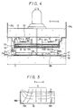
- Fig. 4 shows a cross section thereof in a vertical (Y) direction and in the direction of thickness of the tube.
- a flat type container 15, i.e., a tube is defined by a light transmissive first panel 11, a second panel 12 in opposed relation to the panel 11, and a peripheral wall 13. The interior of the container 15 is kept in high vacuum.
- the first and second panels 11 and 12 are formed from rectangular glass panels.
- the glass peripheral wall 13 consists of four side walls between the glass panels 11 and 12, all three being sealed with glass frit 14 to form the flat type container 15.
- a fluorescent plane 16 is provided on an inner surface of the first panel 11, and is formed by an arrangement of fluorescent segments, for example, red, green and blue fluorescent segments R, G and B.
- the fluorescent plane 16 is formed by arranging a plurality, for example 2 rows and 8 columns, of fluorescent trios, each trio being composed of red, green and blue fluorescent segments R, G and B, giving a total of 48 segments.
- a light absorbing layer 20 such as a carbon coating layer, etc.
- a metal back layer (not shown), such as a Al, vapour-deposition membrane or the like, is formed to cover the whole fluorescent plane.
- An electron beam control mechanism 17 is provided in opposed relation to the fluorescent plane 16 for directing an electron beam to the respective fluorescent segments, R, G and B. Between the electron beam control mechanism 17 and the fluorescent plane 16, a separator electrode 19 is arranged.
- the separator electrode 19 includes partition walls 19A for partitioning spaces in front of the respective fluorescent segments R, G and B to avoid mutual interference of electron beams directed to the respective fluorescent segments R, G and B.
- the separator electrode 19 includes a protruded wall 19B which protrudes from a portion of the partition wall 19A at least in positions in which the fluorescent segments R, G and B are to be arranged in the vicinity of the peripheral wall 13, i.e., along the two sides of the peripheral wall which extend in the horizontal X direction.
- the protruded wall 19B has a height h2 which is higher than the height h1 of the other walls 19A.
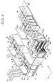
- the separator electrode 19 has, as shown, for example, in Fig. 8, partition walls 19A having a height h1 and the protruded wall 19B having a height h2, higher than h1, formed by punching and bending up of a metal plate.
- the separator electrode 19 has, as shown in Fig. 3, a mounting piece 21 protruding from the peripheral wall which is fixed by, for example, glass frit 50 to the panel 11 and supported thereby.
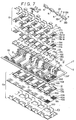
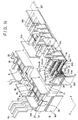
- the electron beam control mechanism 17 provided in opposed relation to the fluorescent plane 16 has, as shown by the partially cut-away main portion in Fig. 6 and by the disassembled perspective view thereof in Fig. 7, a construction in which the cathode K, a first grid G1, a second grid G2 and a third grid G3 are arranged in a plane and in order toward the side of the fluorescent plane 16.
- the third grid G3 is composed of a lamination of a third grid frame F3, made of, for example, a metal plate, and a third grid main body M3 made of a thin metal plate.
- the frame F3 has through-holes H each being common to a trio of the red, green and blue fluorescent segments R, G and B of the fluorescent plane 16.
- the third grid main body M3 is provided with mesh type through-holes H 3R , H 3G and H 3B , formed by photolithography, corresponding in position to the through-holes H F3 of the frame F3 in opposed relation to the respective fluorescent segments R, G and B.
- the third grid main body M3 i mounted on the third grid frame F3 such that the through-holes H 3R , H 3G and H 3B thereof coincide with the through-holes H F3 of the frame F3 and, on the third grid main body, a first insulating spacer S1, made of ceramic or the like, which is common to, for example, four adjacent sets of trios arranged in 2 rows, is mounted.
- the first insulating spacer S1 has through-holes H s1 corresponding to the respective through-holes H F3 of the frame F3 and two protrusions 231 and 232 extend vertically in the Y direction between the through-holes H S1 (in the illustrated example, paired through-holes) in a common column, that is, in a vertical direction Y.
- the second grid G2 is arranged through the respective spacers S1.
- the second grid G2 has strip type parallel electrodes 24R, 24G and 24B common to a column of the respective mesh type through-holes H 3R , H 3G and H 3B of the third grid main body M3.
- the respective strip shaped electrodes 24R, 24G and 24B are formed by photolithography, for example, with paired mesh type through-holes H 2R , H 2G and H 2B corresponding to the paired through-holes H 3R , H 3G and H 3B in a common column in the Y direction of the frame M3.
- Opposite ends of the strip electrodes 24R, 24G and 24B become respective leads 24L, and they are connected at their outer ends by a frame portion 24F to form a lead frame before assembling.
- This lead frame is formed by photolithography, for example.
- the lead frame is mounted on the third grid G3 through the respective spacers S1 such that the protrusions 231 and 232 of the spacers S1 come in between the respective strip electrodes 24R, 24G and 24B, and the frame portion 24F is removed after assembling of the electron beam control mechanism 17 to electrically separate the respective electrodes 24R, 24G and 24B.
- the first grid G1 is mounted through a second insulating spacer S2 which is made of an insulating material such as ceramic or the like and serves also as a cathode support, in a similar manner.
- the second insulating spacer S2 is arranged, in a similar manner to the first insulating spacer S1, to be common to, for example, four adjacent fluorescent trios arranged in two rows and two columns, and has through-holes H s2 corresponding to the respective through-holes H F3 of the frame F3 of the third grid G3.
- paired protrusions 251 and 252 which are integral with the spacer, are provided.
- the respective protrusions 251 and 252 are formed with a cathode support fitting portion 26 comprising a through-hole or groove open end at an end face of the cathode K.
- the first grid G1 is formed by laminating a first grid main body M1, a shield plate S H1 and a first grid frame F1 in order.
- the first grid main body M1 has, for example, mesh type through-holes H 1R , H 1G and H 1B , formed, for example, by photolithography, opposed to the respective mesh type through-holes H 3R , H 3G and H 3B and H 2R , H 2G and H 2B of the third grid G3 and the second grid G2.
- the shield plate SH1 of the first grid G1 is common to four trios each including, for example, mesh type through-holes H 1R , H 1G and H 1B , that is, four adjacent trios arranged in two rows and two columns, and is formed by punching and bending, for example, a metal plate.
- the respective shield plates SH1 are formed with side walls 271 and 272 at positions opposed to the mesh type through-holes H 1R , H 1G and H 1B of the first grid main body M1.
- the side walls 271, 272 extend in the vertical direction Y on both sides of the trio of through-holes H SH1R , H SH1G and H SH1B and are formed by bending up the metal plate.
- Side walls 273 are also formed similarly between the outer ends of the side walls 271, 272 by bending up the metal plate.
- the frame F1 of the first grid can be similarly formed by punching and bending a metal plate common to a plurality of shield plates S H1 .
- the first grid main body M1, the shield plate S H1 and the frame F1 constituting the first grid G1 are mounted sequentially on the second insulating spacer S2 such that the protrusions 251 and 252 of the spacer S2 protrude between the trios of the respective through-holes.
- Metal pieces 28 for mounting the cathode are inserted into the fitting portions 26 of the respective protrusions 251 and 252 of the spacer S2 such that they ride across the end faces of the protrusions 251 and 252 of adjacent through-holes H S2 .
- the cathode K takes the form of, for example, cathode material affixed by, for example, spraying it on a spiral heater extending, for example, linearly, and has opposite ends directly welded to the metal pieces 28.
- the cathode can be formed, as shown in Fig. 7, by initially extending the cathode heater tightly on, for example, a cathode support member 29 and, after spraying with cathode material, welding the metal pieces 28 to the opposite ends of the cathode heater and then cutting the cathode holder 29 at a position such as is shown by the chain line a between the opposite ends of the respective cathodes K to achieve electrical separation between the ends.
- the frame F3, the third grid main body M3 and the first insulating spacer S1 constituting the third grid G3, the lead frame F2 and the second insulating spacer S2 constituting the second grid G2, the first grid main body M1, and the shield plate S H1 and the frame F1 constituting the first grid G1 are stacked in order and caulked together with metal grommets (not shown) through the respective through-holes thereof.
- the insertion holes of the first grid G1 and the third grid G3 for the grommets for caulking are made larger in size alternately so that no electrical connection is provided by the metal grommets between the respective grids G1 - G3.
- the electron beam control mechanism 17 formed by integrating the cathode K and the first to third grids G1 - G3 as a unit is supported mechanically by leading out the leads 24L of the second grid G2 through the frit portion between the panel 12 and the peripheral wall 13, and the lead is derived externally of the container 15.
- the frame portion 24F of the lead frame F2 constituting the second grid G2 is provided with a lead 31 which is connected to a terminal of the cathode K or the third and first grids G3 and G1 and welded to the electrodes G1, G3 corresponding thereto or the cathode holder 29 or the metal piece 28 in assembling the electron beam control mechanism 17.
- the lead 31 is derived, together with the leads 24L, through the frit portion of the container 15 as shown in Fig. 3.
- a rear surface electrode 32 is formed, for example by a carbon coating layer etc., and is electrically connected to the first grid G1 by a resilient contact of a metal resilient piece 33 mounted on, for example, the first grid G1.
- a high voltage lead 34 penetrates a centre portion, for example, of the flat type container 15.
- the inner end of the lead 34 is electrically connected to the separator electrode 19 to derive a terminal.
- a high voltage for example 5 KV
- a voltage for example of 10 V
- a low potential for example 0 V
- a voltage is selectively applied through the lead 24L which voltage is 15 V when it is in the ON state and -2 V when it is in the OFF state.
- the respective fluorescent segments By modulating respective electron beams toward the respective fluorescent segments R, G and B by means of this ON, OFF switching of voltage to the strip electrodes 24R, 24G and 24B of the second grid G2 and selection of voltage applied to the cathode K, the respective fluorescent segments emit light in, for example, line sequence.
- the fluorescent display tube described above can provide a colour display on a large screen by arranging a number of such tubes in a flat plane as mentioned with respect to Figs. 1 and 2.
- a low potential for example O V
- O V a low potential
- an anode voltage that is a fluorescent plane voltage, which is a high voltage of, for example, 5 KV
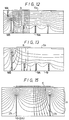
- equipotential lines in front of the separator electrode 19 are bent relatively substantially in the vicinity of the protruded side wall 19B of the separator electrode 19 as shown schematically by thin line a in Fig. 5.
- An electron beam b entering into this portion is deflected outwardly, that is toward the protruded side wall 19B, with respect to the vertical Y direction. That is, the range of possible electron beam impingement on the first panel 11 is enlarged.
- one purpose of the separator electrode 19 is to avoid mutual interference of electron beams directed toward the respective fluorescent segments R, G and B and the respective electron beams follow substantially straight lines in emitting directions from the electron beam control mechanism 17 toward the respective fluorescent segments R, G and B without being considerably deflected by the separator electrode 19.
- the beam diverges towards the peripheral wall 13.
- the electron beam is deflected towards the protruded side wall 19B to which the high voltage is applied to thereby diverge the electron beam. It is therefore possible to arrange the fluorescent segments in positions very close to the peripheral wall 13. Therefore, as described with reference to Fig. 1, where a large screen display device is constructed by arranging a plurality of adjacent fluorescent display tubes 1, the interval De between the adjacent fluorescent segments (trios), and hence the interval Ds, can be small enough, resulting in high resolution.
- the separator electrode 19 is not limited to the particular example shown in Fig. 8 referred to above. It is possible to use a construction in which the height is gradually changed from the protruded side wall 19B having height h2 to the partition wall 19A having height hl as shown in Fig. 9. Further, although, in the examples shown in Figs. 8 and 9, a set of separator electrodes 19 is common to the fluorescent segments on respective lines, it is possible to provide a set of separator electrodes 19 for each trio as shown in Fig. 10, or to provide a set of separator electrodes 19 for a plurality of trios.
- the reduction of the interval De is performed by enlarging the electron beam impinging range in only the vertical direction Y, it is possible to obtain a similar construction in the horizontal X direction by combining it with means for varying a segment pitch of the electrode portion.
- the above described example relates to a colour display in which the respective fluorescent segments are formed by red, green and blue fluorescent segments R, G and B
- the invention can be applied to monochromatic or various colour displays.
- the flat type container 15 is formed by the first and second panels 11 and 12 and the peripheral wall 13 all of which are welded by frit, it can be modified in various ways, for example, by constituting the peripheral wall 13 and, for example, the first panel 11 as a unit.
- a protruded side wall 19B is provided on the separator 19 in a portion of the container 15 in which fluorescent segments R, G and B are arranged in the vicinity of a peripheral side wall 13, and in particular on both sides of the container in the horizontal direction X.
- the protruded side wall 19B is arranged in opposed relation to the peripheral side wall 13, and has a height h2 which is larger than that of the partition walls 19A in other portions of the separator.
- a protruded side wall 18A is provided on a low voltage electrode (in the example shown, a third grid G3) of an electron beam control mechanism 17.
- the protruded side wall 18A extends along the peripheral side wall 13 and towards the separator electrode 19.
- the provision of the separator electrode 19, to which an anode voltage (that is, a fluorescent plane voltage) which is a high voltage of, for example, 5 KV is applied, and the protruded side walls 19B and 18A on the separator 19 and the low voltage electrode G3 arranged in opposed relation to the peripheral side walls 13, enables the influence of electric field due to the peripheral side wall 13 on the electron beam path, and also distortion of electron beam path, to be avoided. That is, where the influence of the peripheral side wall 13 is reduced by providing only the protruded side wall 19B on the separator electrode 19 to which a high voltage is applied, the equipotential lines in the vicinity of the protruded side wall 19B may be sharply bent as shown in Fig.
- the protruded side wall 18A on the low voltage electrode for example the third grid G3, to which a low voltage is applied subjects the electron beam b to an inward deflection as shown in Fig. 12, and it is possible to cancel the deflection due to the protruded side wall 19B to which a high voltage is applied.
- the electron beam b can therefore be substantially straight.
- the present embodiment it is possible to avoid the influence of unstable charge accumulation on a glass plane of the peripheral side wall 13 of the container 15 on the electron beam path, and to avoid an undesirable electron beam deflection by providing the protruded side walls 19B and 18A on the high voltage separator electrode 19 and the low voltage electrode G3 in the fluorescent tube. Therefore, it is possible to reduce the interval De mentioned with respect to Fig. 1 and to thereby reduce the interval Ds between adjacent segment trios of each fluorescent display tube.
- resolution is improved and colour deviation etc. due to unstable deflection of the electron beam is avoided, resulting in an image projection with high image quality.
- the protruded side walls 19B and 18A are provided on both sides of the container 15 in the horizontal direction X, that is, extending along the vertical direction Y, it is possible to use a similar construction for side surfaces in other directions.
- a first grid G1 which opposes the cathodes is formed with opposing side walls 271 and 272 extending towards the opposite end portions of respective cathodes K, such that the side walls 271, 272 protrude on either side of the cathode K in directions orthogonal to the extension of the cathode K.
- a low voltage of, for example, 0 V is applied to electrodes on a fluorescent plane side of an electron beam control mechanism 17, for example to a third grid G3, an anode voltage, that is, a fluorescent plane voltage, which is a high voltage of, for example, 5 KV is applied to a separator electrode 19, and a voltage of, for example, 10 V is applied to the first grid G1. Due to the side walls 271 and 272 of the first grid G1 which are at the opposite ends of the cathode K, an electric field which acts to diverge the electron beam outwards is produced in front of the cathode K as shown by the thin line a in Fig. 15.
- an electron beam emitted from the centre of the cathode K is deflected outwardly, so that the electron density in the centre is reduced while that in the opposite end portions is increased. Therefore, a low emission density due to low temperature at the opposite end portions of the cathode K is compensated by the current density distribution. That is, it is possible to obtain a substantially uniform current density throughout the length of the cathode K and, therefore, it is possible to improve the uniformity of light emission in the segments, improve white balance and stabilize the operation. Thus, in a large screen display, it is possible to project an image with high white balance.
Landscapes
- Cathode-Ray Tubes And Fluorescent Screens For Display (AREA)
Claims (2)
- Fluoreszenz-Anzeigeröhre mit:
einer fluoreszierenden Ebene (16) innerhalb eines Gehäuses (15) vom Flachtyp mit voneinander abgewandten ersten und zweiten Platten (11, 12) und einer Randseitenwand (13), wobei die fluoreszierende Ebene (16) durch Anordnen von fluoreszierenden Segmenten (R, G, B) auf einer Innenseite der ersten Platte (11) gebildet ist, einem Elektronenstrahl-Steuermechanismus (17), der gegenüberliegend der fluoreszierenden Ebene (16) zum Richten von Elektronenstrahlen auf die entsprechenden fluoreszierenden Elemente (R, G, B) vorgesehen ist, und einer Separator-Elektrode (19) zwischen der fluoreszierenden Ebene (16) und dem Elektronenstrahl-Steuermechanismus (17) mit Trennwänden (19A) zwischen den fluoreszierenden Elementen (R, G, B), einer hervorstehenden Seitenwand (19B), die an der Separator-Elektrode (19) in einem Abschnitt des Gehäuses (15) vorgesehen ist, in der die fluoreszierenden Elemente (R, G, B) in der Nähe der Randseitenwand (13) vorgesehen sind, wobei die hervorstehende Seitenwand (19B) sich in Richtung des Elektronenstrahl-Steuermechanismus (17) gegenüberliegend der Randseitenwand (13) erstreckt,
dadurch gekennzeichnet,
daß die hervorstehende Seitenwand (19B) eine Höhe (h2) aufweist, die größer ist als die der Trennwände (19A) der Separator-Elektrode (19), und dadurch, daß eine weitere hervorstehende Seitenwand (18A) an einer Niederspannungselektrode (G3) des Elektrodensträhl-Steuermechanismus (17) in dem Abschnitt des Gehäuses (15) vorgesehen ist, in dem die fluoreszierenden Segmente (R, G, B) in der Nähe der Randseitenwand (13) vorgesehen sind, wobei sich die weitere hervorstehende Seitenwand (18A) in Richtung der Separatorelektrode (19) gegenüberliegend der Randseitenwand (13) erstreckt. - Fluoreszenz-Anzeigeröhre nach Anspruch 1,
bei der der Elektronenstrahl-Steuermechanismus (17) Kathoden (K) und Gitter (G1 - G3) zum Richten von Elektronenstrahlen auf die fluoreszierenden Elemente (R, G, B) aufweist, wobei jede Kathode (K) eine Linearkathode (K) für jedes der fluoreszierenden Elemente (R, G, B) oder für mehrere der fluoreszierenden Elemente (R, G, B) gemeinsam aufweist, und bei der Seitenwände (27₁, 27₂) an einem ersten Gitter (G1) der Gitter G1 - G3) gegenüberliegend der Linearkathoden (K) vorgesehen sind, wobei sich die Seitenwände (27₁, 27₂) in Richtung beider Endabschnitte der Linearkathoden (K) erstrecken.
Applications Claiming Priority (7)
| Application Number | Priority Date | Filing Date | Title |
|---|---|---|---|
| JP7493688A JP2699391B2 (ja) | 1988-03-29 | 1988-03-29 | 螢光表示管 |
| JP63074935A JP2751191B2 (ja) | 1988-03-29 | 1988-03-29 | 螢光表示管 |
| JP74936/88 | 1988-03-29 | ||
| JP7493788A JP2751192B2 (ja) | 1988-03-29 | 1988-03-29 | 螢光表示管 |
| JP74935/88 | 1988-03-29 | ||
| JP74937/88 | 1988-03-29 | ||
| PCT/JP1989/000330 WO1989009482A1 (fr) | 1988-03-29 | 1989-03-29 | Tube d'affichage fluorescent |
Publications (3)
| Publication Number | Publication Date |
|---|---|
| EP0365686A1 EP0365686A1 (de) | 1990-05-02 |
| EP0365686A4 EP0365686A4 (en) | 1991-08-21 |
| EP0365686B1 true EP0365686B1 (de) | 1995-11-15 |
Family
ID=27301657
Family Applications (1)
| Application Number | Title | Priority Date | Filing Date |
|---|---|---|---|
| EP89904224A Expired - Lifetime EP0365686B1 (de) | 1988-03-29 | 1989-03-29 | Fluoreszierende anzeigeröhre |
Country Status (5)
| Country | Link |
|---|---|
| US (1) | US5095244A (de) |
| EP (1) | EP0365686B1 (de) |
| KR (1) | KR0125090B1 (de) |
| DE (1) | DE68924828T2 (de) |
| WO (1) | WO1989009482A1 (de) |
Families Citing this family (5)
| Publication number | Priority date | Publication date | Assignee | Title |
|---|---|---|---|---|
| GB2404279A (en) * | 2002-11-21 | 2005-01-26 | Hitachi Ltd | Display device comprising box-type spacers located on scanning electrodes |
| JP2004171968A (ja) * | 2002-11-21 | 2004-06-17 | Hitachi Ltd | 平面型表示装置 |
| US7293879B2 (en) | 2003-10-23 | 2007-11-13 | Hewlett-Packard Development Company, L.P. | Projection screen |
| US7040764B2 (en) * | 2003-10-23 | 2006-05-09 | Hewlett-Packard Development Company, L.P. | Projection system using ambient light |
| US6987610B2 (en) * | 2003-10-23 | 2006-01-17 | Hewlett-Packard Development Company, L.P. | Projection screen |
Family Cites Families (7)
| Publication number | Priority date | Publication date | Assignee | Title |
|---|---|---|---|---|
| JPS60158779A (ja) * | 1984-01-27 | 1985-08-20 | Sony Corp | 表示装置 |
| JPS60253143A (ja) * | 1984-05-28 | 1985-12-13 | Futaba Corp | カラ−蛍光発光管 |
| JPH061674B2 (ja) * | 1984-12-04 | 1994-01-05 | ソニー株式会社 | 螢光表示管 |
| JPH061675B2 (ja) * | 1984-12-04 | 1994-01-05 | ソニー株式会社 | 螢光表示管 |
| JPS61223878A (ja) * | 1985-03-29 | 1986-10-04 | 三菱電機株式会社 | 表示ユニツト |
| JPH0640474B2 (ja) * | 1985-07-08 | 1994-05-25 | 伊勢電子工業株式会社 | 光源用表示管 |
| JP2625727B2 (ja) * | 1987-06-09 | 1997-07-02 | ソニー株式会社 | 螢光表示管 |
-
1989
- 1989-03-24 KR KR1019890003690A patent/KR0125090B1/ko not_active Expired - Fee Related
- 1989-03-29 WO PCT/JP1989/000330 patent/WO1989009482A1/ja not_active Ceased
- 1989-03-29 US US07/445,654 patent/US5095244A/en not_active Expired - Fee Related
- 1989-03-29 DE DE68924828T patent/DE68924828T2/de not_active Expired - Fee Related
- 1989-03-29 EP EP89904224A patent/EP0365686B1/de not_active Expired - Lifetime
Also Published As
| Publication number | Publication date |
|---|---|
| US5095244A (en) | 1992-03-10 |
| WO1989009482A1 (fr) | 1989-10-05 |
| DE68924828T2 (de) | 1996-05-02 |
| KR890015186A (ko) | 1989-10-28 |
| EP0365686A1 (de) | 1990-05-02 |
| DE68924828D1 (de) | 1995-12-21 |
| EP0365686A4 (en) | 1991-08-21 |
| KR0125090B1 (ko) | 1997-12-11 |
Similar Documents
| Publication | Publication Date | Title |
|---|---|---|
| EP0405262B1 (de) | Anzeigevorrichtung mit flachem Bildschirm | |
| US5859508A (en) | Electronic fluorescent display system with simplified multiple electrode structure and its processing | |
| US5565742A (en) | Electronic fluorescent display | |
| EP0133361B1 (de) | Lumineszierende Anzeigerzellen | |
| US4973888A (en) | Image display device | |
| US4727284A (en) | Light source display for a large picture screen | |
| US3882342A (en) | Gas discharge display panel for color picture reproduction | |
| EP0333079B1 (de) | Lichtquellen-Anzeigeröhre | |
| EP0365686B1 (de) | Fluoreszierende anzeigeröhre | |
| HK1009359B (en) | Light source display tube | |
| US4626737A (en) | Mask focusing color picture tube | |
| US4217519A (en) | Isolation busbar for a flat panel display device | |
| EP0434054B1 (de) | Flache Bildanzeigevorrichtung | |
| US4199705A (en) | Modulator structure for a flat panel display device | |
| KR0141700B1 (ko) | 형광 표시판 | |
| US4143296A (en) | Flat panel display device | |
| US4253040A (en) | Cathode structure for a gas discharge display tube | |
| JPH0614395Y2 (ja) | 平形表示装置 | |
| JPS6347108B2 (de) | ||
| JP2751192B2 (ja) | 螢光表示管 | |
| JPH01235152A (ja) | 光源用表示管 | |
| JP2751191B2 (ja) | 螢光表示管 | |
| JP2890571B2 (ja) | 平面型表示装置 | |
| AU638321B2 (en) | Light source display tube | |
| JP2890572B2 (ja) | 平面型表示装置 |
Legal Events
| Date | Code | Title | Description |
|---|---|---|---|
| PUAI | Public reference made under article 153(3) epc to a published international application that has entered the european phase |
Free format text: ORIGINAL CODE: 0009012 |
|
| 17P | Request for examination filed |
Effective date: 19891127 |
|
| AK | Designated contracting states |
Kind code of ref document: A1 Designated state(s): DE FR GB NL |
|
| A4 | Supplementary search report drawn up and despatched |
Effective date: 19910628 |
|
| AK | Designated contracting states |
Kind code of ref document: A4 Designated state(s): DE FR GB NL |
|
| 17Q | First examination report despatched |
Effective date: 19930906 |
|
| GRAA | (expected) grant |
Free format text: ORIGINAL CODE: 0009210 |
|
| AK | Designated contracting states |
Kind code of ref document: B1 Designated state(s): DE FR GB NL |
|
| REF | Corresponds to: |
Ref document number: 68924828 Country of ref document: DE Date of ref document: 19951221 |
|
| ET | Fr: translation filed | ||
| PLBE | No opposition filed within time limit |
Free format text: ORIGINAL CODE: 0009261 |
|
| STAA | Information on the status of an ep patent application or granted ep patent |
Free format text: STATUS: NO OPPOSITION FILED WITHIN TIME LIMIT |
|
| 26N | No opposition filed | ||
| PGFP | Annual fee paid to national office [announced via postgrant information from national office to epo] |
Ref country code: FR Payment date: 20010313 Year of fee payment: 13 |
|
| PGFP | Annual fee paid to national office [announced via postgrant information from national office to epo] |
Ref country code: DE Payment date: 20010319 Year of fee payment: 13 |
|
| PGFP | Annual fee paid to national office [announced via postgrant information from national office to epo] |
Ref country code: GB Payment date: 20010328 Year of fee payment: 13 |
|
| PGFP | Annual fee paid to national office [announced via postgrant information from national office to epo] |
Ref country code: NL Payment date: 20010330 Year of fee payment: 13 |
|
| REG | Reference to a national code |
Ref country code: GB Ref legal event code: IF02 |
|
| PG25 | Lapsed in a contracting state [announced via postgrant information from national office to epo] |
Ref country code: GB Free format text: LAPSE BECAUSE OF NON-PAYMENT OF DUE FEES Effective date: 20020329 |
|
| PG25 | Lapsed in a contracting state [announced via postgrant information from national office to epo] |
Ref country code: NL Free format text: LAPSE BECAUSE OF NON-PAYMENT OF DUE FEES Effective date: 20021001 Ref country code: DE Free format text: LAPSE BECAUSE OF NON-PAYMENT OF DUE FEES Effective date: 20021001 |
|
| GBPC | Gb: european patent ceased through non-payment of renewal fee |
Effective date: 20020329 |
|
| PG25 | Lapsed in a contracting state [announced via postgrant information from national office to epo] |
Ref country code: FR Free format text: LAPSE BECAUSE OF NON-PAYMENT OF DUE FEES Effective date: 20021129 |
|
| NLV4 | Nl: lapsed or anulled due to non-payment of the annual fee |
Effective date: 20021001 |
|
| REG | Reference to a national code |
Ref country code: FR Ref legal event code: ST |