EP0447327B1 - Dispositif semi-conducteur à hétérostructure - Google Patents
Dispositif semi-conducteur à hétérostructure Download PDFInfo
- Publication number
- EP0447327B1 EP0447327B1 EP91400711A EP91400711A EP0447327B1 EP 0447327 B1 EP0447327 B1 EP 0447327B1 EP 91400711 A EP91400711 A EP 91400711A EP 91400711 A EP91400711 A EP 91400711A EP 0447327 B1 EP0447327 B1 EP 0447327B1
- Authority
- EP
- European Patent Office
- Prior art keywords
- layer
- major surface
- semiconductor device
- substrate
- upper major
- Prior art date
- Legal status (The legal status is an assumption and is not a legal conclusion. Google has not performed a legal analysis and makes no representation as to the accuracy of the status listed.)
- Expired - Lifetime
Links
Images



Classifications
-
- H—ELECTRICITY
- H10—SEMICONDUCTOR DEVICES; ELECTRIC SOLID-STATE DEVICES NOT OTHERWISE PROVIDED FOR
- H10D—INORGANIC ELECTRIC SEMICONDUCTOR DEVICES
- H10D30/00—Field-effect transistors [FET]
- H10D30/40—FETs having zero-dimensional [0D], one-dimensional [1D] or two-dimensional [2D] charge carrier gas channels
- H10D30/47—FETs having zero-dimensional [0D], one-dimensional [1D] or two-dimensional [2D] charge carrier gas channels having two-dimensional [2D] charge carrier gas channels, e.g. nanoribbon FETs or high electron mobility transistors [HEMT]
- H10D30/471—High electron mobility transistors [HEMT] or high hole mobility transistors [HHMT]
- H10D30/473—High electron mobility transistors [HEMT] or high hole mobility transistors [HHMT] having confinement of carriers by multiple heterojunctions, e.g. quantum well HEMT
- H10D30/4732—High electron mobility transistors [HEMT] or high hole mobility transistors [HHMT] having confinement of carriers by multiple heterojunctions, e.g. quantum well HEMT using Group III-V semiconductor material
-
- H—ELECTRICITY
- H10—SEMICONDUCTOR DEVICES; ELECTRIC SOLID-STATE DEVICES NOT OTHERWISE PROVIDED FOR
- H10D—INORGANIC ELECTRIC SEMICONDUCTOR DEVICES
- H10D10/00—Bipolar junction transistors [BJT]
- H10D10/60—Lateral BJTs
-
- H—ELECTRICITY
- H10—SEMICONDUCTOR DEVICES; ELECTRIC SOLID-STATE DEVICES NOT OTHERWISE PROVIDED FOR
- H10D—INORGANIC ELECTRIC SEMICONDUCTOR DEVICES
- H10D62/00—Semiconductor bodies, or regions thereof, of devices having potential barriers
- H10D62/10—Shapes, relative sizes or dispositions of the regions of the semiconductor bodies; Shapes of the semiconductor bodies
- H10D62/17—Semiconductor regions connected to electrodes not carrying current to be rectified, amplified or switched, e.g. channel regions
- H10D62/351—Substrate regions of field-effect devices
- H10D62/357—Substrate regions of field-effect devices of FETs
-
- H—ELECTRICITY
- H10—SEMICONDUCTOR DEVICES; ELECTRIC SOLID-STATE DEVICES NOT OTHERWISE PROVIDED FOR
- H10D—INORGANIC ELECTRIC SEMICONDUCTOR DEVICES
- H10D62/00—Semiconductor bodies, or regions thereof, of devices having potential barriers
- H10D62/80—Semiconductor bodies, or regions thereof, of devices having potential barriers characterised by the materials
- H10D62/82—Heterojunctions
-
- H—ELECTRICITY
- H10—SEMICONDUCTOR DEVICES; ELECTRIC SOLID-STATE DEVICES NOT OTHERWISE PROVIDED FOR
- H10P—GENERIC PROCESSES OR APPARATUS FOR THE MANUFACTURE OR TREATMENT OF DEVICES COVERED BY CLASS H10
- H10P14/00—Formation of materials, e.g. in the shape of layers or pillars
- H10P14/20—Formation of materials, e.g. in the shape of layers or pillars of semiconductor materials
- H10P14/29—Formation of materials, e.g. in the shape of layers or pillars of semiconductor materials characterised by the substrates
- H10P14/2901—Materials
- H10P14/2902—Materials being Group IVA materials
- H10P14/2905—Silicon, silicon germanium or germanium
-
- H—ELECTRICITY
- H10—SEMICONDUCTOR DEVICES; ELECTRIC SOLID-STATE DEVICES NOT OTHERWISE PROVIDED FOR
- H10P—GENERIC PROCESSES OR APPARATUS FOR THE MANUFACTURE OR TREATMENT OF DEVICES COVERED BY CLASS H10
- H10P14/00—Formation of materials, e.g. in the shape of layers or pillars
- H10P14/20—Formation of materials, e.g. in the shape of layers or pillars of semiconductor materials
- H10P14/32—Formation of materials, e.g. in the shape of layers or pillars of semiconductor materials characterised by intermediate layers between substrates and deposited layers
- H10P14/3202—Materials thereof
- H10P14/3214—Materials thereof being Group IIIA-VA semiconductors
- H10P14/3218—Phosphides
-
- H—ELECTRICITY
- H10—SEMICONDUCTOR DEVICES; ELECTRIC SOLID-STATE DEVICES NOT OTHERWISE PROVIDED FOR
- H10P—GENERIC PROCESSES OR APPARATUS FOR THE MANUFACTURE OR TREATMENT OF DEVICES COVERED BY CLASS H10
- H10P14/00—Formation of materials, e.g. in the shape of layers or pillars
- H10P14/20—Formation of materials, e.g. in the shape of layers or pillars of semiconductor materials
- H10P14/32—Formation of materials, e.g. in the shape of layers or pillars of semiconductor materials characterised by intermediate layers between substrates and deposited layers
- H10P14/3202—Materials thereof
- H10P14/3214—Materials thereof being Group IIIA-VA semiconductors
- H10P14/3221—Arsenides
-
- H—ELECTRICITY
- H10—SEMICONDUCTOR DEVICES; ELECTRIC SOLID-STATE DEVICES NOT OTHERWISE PROVIDED FOR
- H10P—GENERIC PROCESSES OR APPARATUS FOR THE MANUFACTURE OR TREATMENT OF DEVICES COVERED BY CLASS H10
- H10P14/00—Formation of materials, e.g. in the shape of layers or pillars
- H10P14/20—Formation of materials, e.g. in the shape of layers or pillars of semiconductor materials
- H10P14/32—Formation of materials, e.g. in the shape of layers or pillars of semiconductor materials characterised by intermediate layers between substrates and deposited layers
- H10P14/3242—Structure
- H10P14/3244—Layer structure
- H10P14/3248—Layer structure consisting of two layers
-
- H—ELECTRICITY
- H10—SEMICONDUCTOR DEVICES; ELECTRIC SOLID-STATE DEVICES NOT OTHERWISE PROVIDED FOR
- H10P—GENERIC PROCESSES OR APPARATUS FOR THE MANUFACTURE OR TREATMENT OF DEVICES COVERED BY CLASS H10
- H10P14/00—Formation of materials, e.g. in the shape of layers or pillars
- H10P14/20—Formation of materials, e.g. in the shape of layers or pillars of semiconductor materials
- H10P14/32—Formation of materials, e.g. in the shape of layers or pillars of semiconductor materials characterised by intermediate layers between substrates and deposited layers
- H10P14/3242—Structure
- H10P14/3244—Layer structure
- H10P14/3251—Layer structure consisting of three or more layers
-
- H—ELECTRICITY
- H10—SEMICONDUCTOR DEVICES; ELECTRIC SOLID-STATE DEVICES NOT OTHERWISE PROVIDED FOR
- H10P—GENERIC PROCESSES OR APPARATUS FOR THE MANUFACTURE OR TREATMENT OF DEVICES COVERED BY CLASS H10
- H10P14/00—Formation of materials, e.g. in the shape of layers or pillars
- H10P14/20—Formation of materials, e.g. in the shape of layers or pillars of semiconductor materials
- H10P14/34—Deposited materials, e.g. layers
- H10P14/3402—Deposited materials, e.g. layers characterised by the chemical composition
- H10P14/3414—Deposited materials, e.g. layers characterised by the chemical composition being group IIIA-VIA materials
- H10P14/3421—Arsenides
Definitions
- the semiconductor devices formed on the foregoing heteroepitaxial structure has a problem of excessive leakage current flowing from the active layer to the substrate.
- leakage current flows, the electric isolation of devices on the substrate is naturally deteriorated.
- the leakage current is large enough to cause poor device isolation, the substrate can no longer be used for the substrate of integrated circuits.
- the side gate effect there occurs an interference between adjacent devices known as the "side gate effect".
- the threshold voltage of a device such as MESFET may change by the gate voltage applied to an adjecent device.
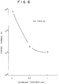
- FIG.6 shows the leakage current measured about the structure of FIG.5(D). The measurement was made by measuring the current flowing between the source and drain in the turned-off state of the HEMT. A number of samples were prepared with the substantially identical structure but changing thickness of the barrier layer 13. As can be seen clearly from FIG.6, the leakage current decreases to about 1/100, as compared to the case where no barrier layer 13 is provided, when the barrier layer 13 is formed with the thickness of 1 ⁇ m. Further, it was shown that the mutual conductance of HEMT, having the normalized gate length of 2 - 10 ⁇ m, is improved from 180 - 230 mS/mm to 250 - 270 mS/mm by the provision of the barrier layer 13. These findings clearly indicate the effect of electrical isolation achieved by the barrier layer 13.
- TMA trimethyl aluminum
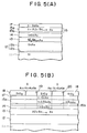
- a silicon oxide layer 18 is deposited on the top surface of the cap layer 17 as shown in FIG.5(B) by a CVD process using silane and oxygen at a temperature of 350 - 450 °C. Further, a photoresist (not shown) is deposited on the silicon oxide layer 18 and patterned subsequently to expose the part of the silicon oxide layer 18 corresponding to the source and drain electrodes of HEMT. After an etching process for removing the exposed part of the silicon oxide layer 18, metal layers of gold-germanium alloy, nickel and gold are deposited consecutively to fill the contact holes formed in the silicon oxide layer 18 in correspondence to the source and drain electrodes.
Landscapes
- Junction Field-Effect Transistors (AREA)
- Recrystallisation Techniques (AREA)
Claims (11)
- Dispositif à semi-conducteur comprenant :un substrat (11) comportant une face principale supérieure et une face principale inférieure ;une couche tampon (12) comportant une face principale supérieure et une face principale inférieure et comprenant une première matière différente de celle du substrat, ladite première matière étant un semi-conducteur à base de composés des groupes III à V ayant une première résistivité, une première constante de réseau et une première largeur de bande interdite, ladite couche tampon (12) étant réalisée de façon épitaxiale sur la face principale supérieure du substrat (11) ;une couche barrière (13) ayant une face principale supérieure et une face principale inférieure et comprenant une deuxième matière différente de celle du substrat, ladite deuxième matière étant un semi-conducteur à base de composés des groupes III à V, ayant une deuxième résistivité sensiblement plus grande que la première résistivité, une deuxième constante de réseau différente de la première constante de réseau, et une largeur de bande interdite sensiblement plus grande que celle de la première bande interdite, la face principale inférieure de ladite couche barrière (13) étant en contact avec la face principale supérieure de la couche tampon (12) ;une couche active (14, 15) comportant une face principale supérieure et une face principale inférieure et disposée sur la face principale supérieure de la couche barrière ; etun dispositif actif (9, 10, 8, 14, 15 ; 14, 15a, 15b, 17, 19, 20, 21) disposé sur la couche active (14) de façon telle qu'au moins une partie du dispositif actif soit formée dans la couche active (14) ;caractérisé en ce qu'au moins la partie de face principale inférieure (14) de la couche active (14, 15) est constituée d'une troisième matière ; en ce que la troisième matière est une matière semi-conductrice à base de composés des groupes III à V ; et en ce que les première, deuxième, et troisième matières sont des matières différentes.
- Dispositif à semi-conducteur selon la revendication 1, caractérisé en ce que ledit substrat est fait d'une matière choisie à partir d'un groupe constitué du silicium, du germanium et de l'oxyde d'aluminium.
- Dispositif à semi-conducteur selon la revendication 1, caractérisé en ce que ladite première matière est choisie à partir d'un groupe constitué de l'arséniure de gallium, du phosphure de gallium et d'un cristal mixte de ceux-ci.
- Dispositif à semi-conducteur selon la revendication 1, caractérisé en ce que ladite deuxième matière est choisie à partir d'un groupe constitué de l'arséniure de gallium et d'aluminium, de l'arséniure d'aluminium et d'indium et d'un cristal mixte de ceux-ci.
- Dispositif à semi-conducteur selon la revendication 4, caractérisé en ce que ladite deuxième matière comprend de l'arséniure de gallium et d'aluminium ayant une composition d'environ Al0,3Ga0,7As.
- Dispositif à semi-conducteur selon la revendication 4, caractérisé en ce que ladite deuxième matière comprend de l'arséniure d'aluminium et d'indium ayant une composition d'environ In0,1Al0,9As.
- Dispositif à semi-conducteur selon la revendication 4, caractérisé en ce que ladite deuxième matière est une matière non dopée.
- Dispositif à semi-conducteur selon la revendication 7, caractérisé en ce que ladite deuxième matière a une résistivité d'au moins 50 Ûcm.
- Dispositif à semi-conducteur selon la revendication 4, caractérisé en ce que ladite seconde matière est dopée par un élément d'impureté qui forme un niveau d'impureté profond dans la troisième matière.
- Dispositif à semi-conducteur selon la revendication 9, caractérisé en ce que ladite deuxième matière a une résistivité d'au moins 100 Ûcm.
- Dispositif à semi-conducteur selon la revendication 1, caractérisé en ce que ladite couche active (14, 15) comprend une couche non dopée (14) d'arséniure d'indium et de gallium ayant une face principale supérieure et une face principale inférieure qui coïncide avec la face principale inférieure de la couche active ; une couche dopée (15) d'arséniure de gallium et d'aluminium et comportant une face principale supérieure et une face principale inférieure et qui est disposée sur la couche non dopée ; un premier moyen formant électrode (9, 19) disposé sur la face principale supérieure de la couche dopée pour injecter des porteurs dans la couche dopée ; un deuxième moyen formant électrode (10, 20) disposé sur la face principale supérieure de la couche dopée avec une séparation par rapport au premier moyen formant électrode pour récupérer les porteurs provenant de la couche dopée ; et un troisième moyen formant électrode (8, 21) disposé sur la face principale supérieure de la couche dopée entre les première et deuxième moyens formant électrode pour commander l'écoulement des porteurs du premier moyen formant électrode vers le deuxième moyen formant électrode.
Applications Claiming Priority (2)
| Application Number | Priority Date | Filing Date | Title |
|---|---|---|---|
| JP65124/90 | 1990-03-15 | ||
| JP2065124A JP2817995B2 (ja) | 1990-03-15 | 1990-03-15 | ▲iii▼―▲v▼族化合物半導体ヘテロ構造基板および▲iii▼―▲v▼族化合物ヘテロ構造半導体装置 |
Publications (3)
| Publication Number | Publication Date |
|---|---|
| EP0447327A2 EP0447327A2 (fr) | 1991-09-18 |
| EP0447327A3 EP0447327A3 (en) | 1992-01-15 |
| EP0447327B1 true EP0447327B1 (fr) | 1996-06-12 |
Family
ID=13277814
Family Applications (1)
| Application Number | Title | Priority Date | Filing Date |
|---|---|---|---|
| EP91400711A Expired - Lifetime EP0447327B1 (fr) | 1990-03-15 | 1991-03-15 | Dispositif semi-conducteur à hétérostructure |
Country Status (4)
| Country | Link |
|---|---|
| US (1) | US5144379A (fr) |
| EP (1) | EP0447327B1 (fr) |
| JP (1) | JP2817995B2 (fr) |
| DE (1) | DE69120116T2 (fr) |
Families Citing this family (41)
| Publication number | Priority date | Publication date | Assignee | Title |
|---|---|---|---|---|
| US5130269A (en) * | 1988-04-27 | 1992-07-14 | Fujitsu Limited | Hetero-epitaxially grown compound semiconductor substrate and a method of growing the same |
| US5351128A (en) * | 1991-08-02 | 1994-09-27 | Hitachi, Ltd. | Semiconductor device having reduced contact resistance between a channel or base layer and a contact layer |
| FR2689683B1 (fr) * | 1992-04-07 | 1994-05-20 | Thomson Composants Microondes | Dispositif semiconducteur a transistors complementaires. |
| EP0603780B1 (fr) * | 1992-12-21 | 1998-04-29 | Nippon Steel Corporation | Procédé de croissance d'un semi-conducteur composé sur une pastille de silicium |
| JP3036404B2 (ja) * | 1995-05-25 | 2000-04-24 | 株式会社村田製作所 | 半導体装置とその製造方法 |
| US5621227A (en) * | 1995-07-18 | 1997-04-15 | Discovery Semiconductors, Inc. | Method and apparatus for monolithic optoelectronic integrated circuit using selective epitaxy |
| US6423990B1 (en) | 1997-09-29 | 2002-07-23 | National Scientific Corporation | Vertical heterojunction bipolar transistor |
| US5912481A (en) * | 1997-09-29 | 1999-06-15 | National Scientific Corp. | Heterojunction bipolar transistor having wide bandgap, low interdiffusion base-emitter junction |
| US6380601B1 (en) | 1999-03-29 | 2002-04-30 | Hughes Electronics Corporation | Multilayer semiconductor structure with phosphide-passivated germanium substrate |
| GB2351841A (en) | 1999-07-06 | 2001-01-10 | Sharp Kk | A semiconductor laser device |
| US6653706B1 (en) | 2000-05-08 | 2003-11-25 | The Board Of Trustees Of The Leland Stanford Junior University | Low temperature grown optical detector |
| US6512369B2 (en) * | 2001-05-22 | 2003-01-28 | Delphi Technologies, Inc. | Temperature compensated voltage divider with a magnetoresistor and a reference resistor |
| JP2003007976A (ja) * | 2001-06-25 | 2003-01-10 | Mitsubishi Electric Corp | 半導体装置及びモジュール装置 |
| US6815790B2 (en) * | 2003-01-10 | 2004-11-09 | Rapiscan, Inc. | Position sensing detector for the detection of light within two dimensions |
| US8164151B2 (en) * | 2007-05-07 | 2012-04-24 | Osi Optoelectronics, Inc. | Thin active layer fishbone photodiode and method of manufacturing the same |
| US7880258B2 (en) * | 2003-05-05 | 2011-02-01 | Udt Sensors, Inc. | Thin wafer detectors with improved radiation damage and crosstalk characteristics |
| US7656001B2 (en) * | 2006-11-01 | 2010-02-02 | Udt Sensors, Inc. | Front-side illuminated, back-side contact double-sided PN-junction photodiode arrays |
| US7655999B2 (en) * | 2006-09-15 | 2010-02-02 | Udt Sensors, Inc. | High density photodiodes |
| US7057254B2 (en) * | 2003-05-05 | 2006-06-06 | Udt Sensors, Inc. | Front illuminated back side contact thin wafer detectors |
| US8035183B2 (en) * | 2003-05-05 | 2011-10-11 | Udt Sensors, Inc. | Photodiodes with PN junction on both front and back sides |
| US7576369B2 (en) * | 2005-10-25 | 2009-08-18 | Udt Sensors, Inc. | Deep diffused thin photodiodes |
| US7242069B2 (en) * | 2003-05-05 | 2007-07-10 | Udt Sensors, Inc. | Thin wafer detectors with improved radiation damage and crosstalk characteristics |
| US7709921B2 (en) | 2008-08-27 | 2010-05-04 | Udt Sensors, Inc. | Photodiode and photodiode array with improved performance characteristics |
| US8766392B2 (en) * | 2007-05-07 | 2014-07-01 | Osi Optoelectronics, Inc. | Thin active layer fishbone photodiode with a shallow N+ layer and method of manufacturing the same |
| US7279731B1 (en) | 2006-05-15 | 2007-10-09 | Udt Sensors, Inc. | Edge illuminated photodiodes |
| US8519503B2 (en) * | 2006-06-05 | 2013-08-27 | Osi Optoelectronics, Inc. | High speed backside illuminated, front side contact photodiode array |
| US7256470B2 (en) * | 2005-03-16 | 2007-08-14 | Udt Sensors, Inc. | Photodiode with controlled current leakage |
| US8686529B2 (en) | 2010-01-19 | 2014-04-01 | Osi Optoelectronics, Inc. | Wavelength sensitive sensor photodiodes |
| US8120023B2 (en) | 2006-06-05 | 2012-02-21 | Udt Sensors, Inc. | Low crosstalk, front-side illuminated, back-side contact photodiode array |
| JP2008527687A (ja) * | 2004-12-30 | 2008-07-24 | オーミック ソシエテ パール アクション サンプリフィエ | エンハンスメント−デプレッション半導体構造及びその製造方法 |
| JP2007149794A (ja) * | 2005-11-25 | 2007-06-14 | Matsushita Electric Ind Co Ltd | 電界効果トランジスタ |
| US9178092B2 (en) | 2006-11-01 | 2015-11-03 | Osi Optoelectronics, Inc. | Front-side illuminated, back-side contact double-sided PN-junction photodiode arrays |
| US9006707B2 (en) * | 2007-02-28 | 2015-04-14 | Intel Corporation | Forming arsenide-based complementary logic on a single substrate |
| US20100053802A1 (en) * | 2008-08-27 | 2010-03-04 | Masaki Yamashita | Low Power Disk-Drive Motor Driver |
| US7687799B2 (en) * | 2008-06-19 | 2010-03-30 | Intel Corporation | Methods of forming buffer layer architecture on silicon and structures formed thereby |
| US8399909B2 (en) * | 2009-05-12 | 2013-03-19 | Osi Optoelectronics, Inc. | Tetra-lateral position sensing detector |
| US8912615B2 (en) | 2013-01-24 | 2014-12-16 | Osi Optoelectronics, Inc. | Shallow junction photodiode for detecting short wavelength light |
| CN105424234A (zh) * | 2015-12-01 | 2016-03-23 | 成都嘉石科技有限公司 | 一种压力传感器集成器件及其制作方法 |
| DE102018108604A1 (de) * | 2018-04-11 | 2019-10-17 | Aixtron Se | Nukleationsschicht-Abscheideverfahren |
| US12166102B2 (en) | 2020-12-18 | 2024-12-10 | Innoscience (Suzhou) Technology Co., Ltd. | Semiconductor device and method for manufacturing the same |
| US12027615B2 (en) | 2020-12-18 | 2024-07-02 | Innoscience (Suzhou) Technology Co., Ltd. | Semiconductor device and method for manufacturing the same |
Family Cites Families (8)
| Publication number | Priority date | Publication date | Assignee | Title |
|---|---|---|---|---|
| US4157556A (en) * | 1977-01-06 | 1979-06-05 | Varian Associates, Inc. | Heterojunction confinement field effect transistor |
| JPS6012724A (ja) * | 1983-07-01 | 1985-01-23 | Agency Of Ind Science & Technol | 化合物半導体の成長方法 |
| EP0200933B1 (fr) * | 1985-04-05 | 1992-11-04 | Nec Corporation | Transistor à hétérojonction ayant des caractéristiques bipolaires |
| US4916498A (en) * | 1985-09-15 | 1990-04-10 | Trw Inc. | High electron mobility power transistor |
| US4745448A (en) * | 1985-12-24 | 1988-05-17 | Raytheon Company | Semiconductor devices having compensated buffer layers |
| JPH0783028B2 (ja) * | 1986-06-02 | 1995-09-06 | 株式会社日立製作所 | 半導体装置及び製造方法 |
| US4827320A (en) * | 1986-09-19 | 1989-05-02 | University Of Illinois | Semiconductor device with strained InGaAs layer |
| US4987463A (en) * | 1989-08-28 | 1991-01-22 | Motorola, Inc. | FET having a high trap concentration interface layer |
-
1990
- 1990-03-15 JP JP2065124A patent/JP2817995B2/ja not_active Expired - Fee Related
-
1991
- 1991-03-15 US US07/669,980 patent/US5144379A/en not_active Expired - Fee Related
- 1991-03-15 DE DE69120116T patent/DE69120116T2/de not_active Expired - Fee Related
- 1991-03-15 EP EP91400711A patent/EP0447327B1/fr not_active Expired - Lifetime
Non-Patent Citations (1)
| Title |
|---|
| PATENT ABSTRACTS OF JAPAN vol. 10, no. 283 (E-440)(2339) ; & JP-A-61 102 069 * |
Also Published As
| Publication number | Publication date |
|---|---|
| EP0447327A3 (en) | 1992-01-15 |
| DE69120116T2 (de) | 1996-10-24 |
| JPH03266439A (ja) | 1991-11-27 |
| EP0447327A2 (fr) | 1991-09-18 |
| US5144379A (en) | 1992-09-01 |
| JP2817995B2 (ja) | 1998-10-30 |
| DE69120116D1 (de) | 1996-07-18 |
Similar Documents
| Publication | Publication Date | Title |
|---|---|---|
| US5144379A (en) | Semiconductor device having a group iii-v epitaxial semiconductor layer on a substrate | |
| EP0331467B1 (fr) | Méthode pour former une couche mince semi-conductrice | |
| EP0365875B1 (fr) | Recuit sous encapsulant | |
| US5238869A (en) | Method of forming an epitaxial layer on a heterointerface | |
| EP0442414B1 (fr) | Substrat composé à semi-conducteur et procédé pour sa fabrication | |
| US20060043419A1 (en) | Semiconductor substrate and semiconductor device manufactured by epitaxial growth on the semiconductor substrate | |
| EP0352472A2 (fr) | Hétéroépitaxie de matériaux semiconducteurs à résaux inégaux | |
| EP0740350B1 (fr) | Dispositif semi-conducteur composé à résistance réduite | |
| EP0206787B1 (fr) | Transistor bipolaire à hétérojonction et sa méthode de fabrication | |
| EP0430562B1 (fr) | Hétérostructure semi-conductrice et méthode pour sa fabrication | |
| EP0249371B1 (fr) | Dispositif semi-conducteur comprenant deux semi-conducteurs composés et sa méthode de fabrication | |
| US4902643A (en) | Method of selective epitaxial growth for compound semiconductors | |
| US4837178A (en) | Method for producing a semiconductor integrated circuit having an improved isolation structure | |
| JP4429459B2 (ja) | 高抵抗GaN結晶層の製造方法 | |
| US5017517A (en) | Method of fabricating semiconductor device using an Sb protection layer | |
| US6043143A (en) | Ohmic contact and method of manufacture | |
| JP3227083B2 (ja) | バイポーラトランジスタの作製方法 | |
| JP2808671B2 (ja) | 電界効果トランジスタ | |
| JP3670130B2 (ja) | Iii−v族化合物半導体装置の製造方法 | |
| JP2770586B2 (ja) | ヘテロ接合バイポーラトランジスタの製造方法 | |
| JPH025439A (ja) | 半導体基板 | |
| JPH0620968A (ja) | 元素半導体基板上の金属膜/化合物半導体積層構造およびその製造方法 | |
| JPH0864613A (ja) | 半導体装置及びその製造方法 | |
| JPH08111380A (ja) | 半導体構造作製法 | |
| JPH06268279A (ja) | ヘテロ接合ホール素子 |
Legal Events
| Date | Code | Title | Description |
|---|---|---|---|
| PUAI | Public reference made under article 153(3) epc to a published international application that has entered the european phase |
Free format text: ORIGINAL CODE: 0009012 |
|
| AK | Designated contracting states |
Kind code of ref document: A2 Designated state(s): DE FR GB |
|
| PUAL | Search report despatched |
Free format text: ORIGINAL CODE: 0009013 |
|
| AK | Designated contracting states |
Kind code of ref document: A3 Designated state(s): DE FR GB |
|
| 17P | Request for examination filed |
Effective date: 19920615 |
|
| 17Q | First examination report despatched |
Effective date: 19940419 |
|
| GRAA | (expected) grant |
Free format text: ORIGINAL CODE: 0009210 |
|
| AK | Designated contracting states |
Kind code of ref document: B1 Designated state(s): DE FR GB |
|
| REF | Corresponds to: |
Ref document number: 69120116 Country of ref document: DE Date of ref document: 19960718 |
|
| ET | Fr: translation filed | ||
| PLBE | No opposition filed within time limit |
Free format text: ORIGINAL CODE: 0009261 |
|
| STAA | Information on the status of an ep patent application or granted ep patent |
Free format text: STATUS: NO OPPOSITION FILED WITHIN TIME LIMIT |
|
| 26N | No opposition filed | ||
| REG | Reference to a national code |
Ref country code: GB Ref legal event code: IF02 |
|
| PGFP | Annual fee paid to national office [announced via postgrant information from national office to epo] |
Ref country code: FR Payment date: 20030310 Year of fee payment: 13 |
|
| PGFP | Annual fee paid to national office [announced via postgrant information from national office to epo] |
Ref country code: GB Payment date: 20030312 Year of fee payment: 13 |
|
| PGFP | Annual fee paid to national office [announced via postgrant information from national office to epo] |
Ref country code: DE Payment date: 20030327 Year of fee payment: 13 |
|
| PG25 | Lapsed in a contracting state [announced via postgrant information from national office to epo] |
Ref country code: GB Free format text: LAPSE BECAUSE OF NON-PAYMENT OF DUE FEES Effective date: 20040315 |
|
| PG25 | Lapsed in a contracting state [announced via postgrant information from national office to epo] |
Ref country code: DE Free format text: LAPSE BECAUSE OF NON-PAYMENT OF DUE FEES Effective date: 20041001 |
|
| GBPC | Gb: european patent ceased through non-payment of renewal fee |
Effective date: 20040315 |
|
| PG25 | Lapsed in a contracting state [announced via postgrant information from national office to epo] |
Ref country code: FR Free format text: LAPSE BECAUSE OF NON-PAYMENT OF DUE FEES Effective date: 20041130 |
|
| REG | Reference to a national code |
Ref country code: FR Ref legal event code: ST |