EP0366332B1 - Système de mémoire numérique - Google Patents
Système de mémoire numérique Download PDFInfo
- Publication number
- EP0366332B1 EP0366332B1 EP89310644A EP89310644A EP0366332B1 EP 0366332 B1 EP0366332 B1 EP 0366332B1 EP 89310644 A EP89310644 A EP 89310644A EP 89310644 A EP89310644 A EP 89310644A EP 0366332 B1 EP0366332 B1 EP 0366332B1
- Authority
- EP
- European Patent Office
- Prior art keywords
- bitline
- transistor
- pullup
- memory cell
- sense amplifier
- Prior art date
- Legal status (The legal status is an assumption and is not a legal conclusion. Google has not performed a legal analysis and makes no representation as to the accuracy of the status listed.)
- Expired - Lifetime
Links
- 230000015654 memory Effects 0.000 title claims description 67
- 230000003068 static effect Effects 0.000 claims description 14
- 238000000034 method Methods 0.000 claims description 10
- 230000006870 function Effects 0.000 claims description 7
- 229910001218 Gallium arsenide Inorganic materials 0.000 claims description 3
- 230000002708 enhancing effect Effects 0.000 claims description 3
- 230000001419 dependent effect Effects 0.000 claims description 2
- JBRZTFJDHDCESZ-UHFFFAOYSA-N AsGa Chemical compound [As]#[Ga] JBRZTFJDHDCESZ-UHFFFAOYSA-N 0.000 claims 1
- 230000005669 field effect Effects 0.000 claims 1
- 238000013461 design Methods 0.000 description 9
- 230000004044 response Effects 0.000 description 8
- 238000005094 computer simulation Methods 0.000 description 3
- 230000009977 dual effect Effects 0.000 description 3
- 239000004065 semiconductor Substances 0.000 description 3
- 230000003321 amplification Effects 0.000 description 2
- 239000000463 material Substances 0.000 description 2
- 238000003199 nucleic acid amplification method Methods 0.000 description 2
- 230000009466 transformation Effects 0.000 description 2
- 238000006243 chemical reaction Methods 0.000 description 1
- 230000000295 complement effect Effects 0.000 description 1
- 230000008878 coupling Effects 0.000 description 1
- 238000010168 coupling process Methods 0.000 description 1
- 238000005859 coupling reaction Methods 0.000 description 1
- 238000011156 evaluation Methods 0.000 description 1
- 238000002955 isolation Methods 0.000 description 1
- 238000012986 modification Methods 0.000 description 1
- 230000008569 process Effects 0.000 description 1
- 230000035945 sensitivity Effects 0.000 description 1
- 229910052710 silicon Inorganic materials 0.000 description 1
- 239000010703 silicon Substances 0.000 description 1
- 238000004088 simulation Methods 0.000 description 1
- 238000006467 substitution reaction Methods 0.000 description 1
- 238000012546 transfer Methods 0.000 description 1
Images

Classifications
-
- G—PHYSICS
- G11—INFORMATION STORAGE
- G11C—STATIC STORES
- G11C7/00—Arrangements for writing information into, or reading information out from, a digital store
- G11C7/06—Sense amplifiers; Associated circuits, e.g. timing or triggering circuits
- G11C7/065—Differential amplifiers of latching type
-
- G—PHYSICS
- G11—INFORMATION STORAGE
- G11C—STATIC STORES
- G11C11/00—Digital stores characterised by the use of particular electric or magnetic storage elements; Storage elements therefor
- G11C11/21—Digital stores characterised by the use of particular electric or magnetic storage elements; Storage elements therefor using electric elements
- G11C11/34—Digital stores characterised by the use of particular electric or magnetic storage elements; Storage elements therefor using electric elements using semiconductor devices
- G11C11/40—Digital stores characterised by the use of particular electric or magnetic storage elements; Storage elements therefor using electric elements using semiconductor devices using transistors
- G11C11/41—Digital stores characterised by the use of particular electric or magnetic storage elements; Storage elements therefor using electric elements using semiconductor devices using transistors forming static cells with positive feedback, i.e. cells not needing refreshing or charge regeneration, e.g. bistable multivibrator or Schmitt trigger
- G11C11/413—Auxiliary circuits, e.g. for addressing, decoding, driving, writing, sensing, timing or power reduction
- G11C11/417—Auxiliary circuits, e.g. for addressing, decoding, driving, writing, sensing, timing or power reduction for memory cells of the field-effect type
- G11C11/419—Read-write [R-W] circuits
-
- G—PHYSICS
- G11—INFORMATION STORAGE
- G11C—STATIC STORES
- G11C7/00—Arrangements for writing information into, or reading information out from, a digital store
- G11C7/12—Bit line control circuits, e.g. drivers, boosters, pull-up circuits, pull-down circuits, precharging circuits, equalising circuits, for bit lines
Definitions
- This invention relates to digital memory systems and, more specifically, to a high speed static random access memory (RAM) system.
- RAM static random access memory
- V It/C
- I the bitline charging current
- C the bitline capacitance
- EP-A-0 239 021 there is disclosed a semiconductor memory device having memory cells in a plurality of columns connected to pairs of bitlines. Each bitline receives current from a pullup transistor. Each pair of bitlines is connected through a column transfer gate operated by column address signals to a sense amplifier and to a write circuit including a clamp circuit for clamping a driving level.
- JP-A-58-179990 there is described a sense amplifying circuit having a pair of cross-connected FET's with transistor current sources as loads across which the amplified output signals are developed.
- the sources and gates of the cross-connected FET's are connected to the outputs of two other FET amplifiers, to the gates of which two lines receiving complementary signals to be amplified are respectively connected.
- JP-A-61-208693 discloses a 6-transistor memory cell for a random access memory using MESFET's.
- Single transistor current sources are respectively connected to two bitlines which are connected to ground through respective diodes, and to which the memory cell is connected through its gate transistors that are controlled by a word line signal.
- a digital memory system comprising: at least a first column of memory cells; a plurality of word lines respectively connected to the memory cells to enable electrical signals to be applied to a selected memory cell; a first bitline connected to each memory cell in the column for electrical signals determining the state of the selected cell; a bitline pullup transistor connectable to a source of electrical power and connected to function as a current source for the bitline and sense amplifying means connected to the bitline to provide an output signal corresponding to the state of the corresponding memory cell characterised in that the sense amplifying means comprises a transistor having its controlled current path connected between the bitline and the bitline pull up transistor 18 to provide at its connection to the bitline pullup transistor a signal corresponding to the state of a selected memory cell; and in that the system further comprises biasing means for biasing the gate of the transistor of the sense amplifying means so that the bias applied is low when the potential on the bitline is high and the bias is high when the potential is low.
- the system includes a column of memory cells and a plurality of word lines connected for selecting a memory cell.
- a bitline is connected to each memory cell in the column and a bitline pullup transistor having first, second and third terminals is arranged to form a current source at the second terminal.
- First and second source/drain electrodes of an amplifier transistor are connected to the second terminal of the pullup transistor and the bitline respectively.
- the gate electrode of the amplifier transistor is connected to receive a bias voltage.
- An amplified bitline signal corresponding to the state of a selected memory cell is available at an output node between the pullup and amplifier transistors.
- the preferred embodiment of the memory system includes first and second bitlines connected to each memory cell in the column.
- a bitline pullup transistor and an amplifier transistor are associated with each bit line as described above.
- An output node between the first pullup and amplifier transistors provides an amplified bitline signal corresponding to the state of a selected memory cell while a second output node between the second pullup transistor and the second amplifier transistor provides an amplified bitline signal corresponding to the inverted state of a selected memory cell.
- a digital memory system comprising at least a first column of memory cells, a plurality of word lines respectively connected to the memory cells to enable electrical signals to be applied to a selected memory cell in the first column, first and second bitlines conected to each memory cell in the first column for electrical signals determining the state of the selected memory cell, first and second bitline pullup transistors connectable to a source of electrical power and respectively arranged to provide currents for the first and second bitlines, and sense amplifying means connected to the first and second bitlines for providing at least one output signal corresponding to the state of the selected memory cell, characterised in that the sense amplifying means comprises two transistors, the first transistor having its controlled current path connected between the first bit line pullup transistor and the first bit line and its gate connected to the second bit line, the second transistor having its controlled current path connected between the second bit line pullup transistor and the second bit line and its gate connected to the first bit line; and the at least one output signal is provided at at least one of the connections of the transistors of
- a method for enhancing high speed operation of a static random access memory system including at least a first column of memory cells, a plurality of word lines and bitlines connected for memory cell selection, a bitline pullup transistor and a sense amplifier transistor connected to a bitline, the method comprising the steps of feeding a charging current from the bitline pullup transistor to the bitline (BL1) through the sense amplifier transistor, biasing the gate of the sense amplifier transistor with a low bias when the potential on the bitline is high and with a high bias when the potential on the bitline is low, and deriving a signal corresponding to the state of the selected memory cell from the connection of the sense amplifier transistor to the bitline pullup transistor so as to isolate the capacitance of the bitline (BL1) from the associated bitline pullup transistor dependent on the low or high bias.
- bitline current could be used to generate a sufficiently large signal, a simpler, lower power, faster system would be available.
- speed requirements of high density memories preclude obtaining the full amplitude signal directly from the bitlines.
- a merged bitline pullup - sense amplifier circuit provides an impedance transformation, i.e., a current to voltage conversion of the bitline signal. This results in a highly amplified voltage output signal indicative of the state of a selected memory cell.
- Figure 1 is a partial schematic view of a high speed static RAM device 10 comprising a merged bitline pullup - sense amplifier circuit in conjunction with an exemplary column of 64 memory cells 12.
- the device 10 is presented in simplified form to more clearly describe the invention, it is to be understood that the device includes numerous additional components present in conventional static RAM architecture such as row and column address circuitry, decode logic and output circuitry. See U.S. Patent No. 4,665,508.
- the device 10 may be a 4K GaAs MESFET Static RAM containing 4,096 memory cells organized in a 64 row by 64 column array.
- Decoding may be implemented with a single level of 64 six-input NOR gates.
- the decoded 6-bit row and column addresses enable the word lines and select a particular column of memory cells. Data are sequentially written into or read out of selected memory cells in accordance with the state of the write enable, data in and chip select signals.
- the memory cells 12 illustrated in Figure 1 may each be, for example, of a conventional six transistor design including two cross-coupled switching transistors, two load transistors and a pair of pass transistors.
- a plurality of word lines WL i and bitlines BL i are connected for memory cell selection.
- bitlines BL1 and BL2 are coupled to the memory cells 12 along opposing sides of the column.
- the bitlines are coupled to a power supply line V DD by bitline pullup - sense amplifier circuitry which includes a pair of dual function pullup/load transistors 18 and 20 as well as a pair of amplifier transistors 22 and 24 each positioned between a bitline and one of the dual function transistors 18 or 20.
- An amplifier output node 28 or 30 is located between each dual function transistor 18 or 20 and an adjacent amplifier transistor 22 or 24.
- the amplifier transistors 22 and 24 are positioned to isolate the bitline capacitance from the output nodes 28 and 30. With this isolation each transistor 18 and 20 serves as the load to an adjacent amplifier transistor. The arrangement enables a very fast amplified output to be developed at the output nodes 28 and 30.
- each amplifier transistor 22 and 24 is connected to an opposing bitline and all four transistors 18, 20, 22 and 24 are depletion mode MESFETs.
- the transistors 18 and 20 are each arranged with the drain electrode coupled to V DD and the gate tied to the source electrode thereby providing a current source.
- a clamping diode 42 may be serially connected between each bitline and a reference potential 44.
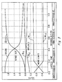
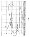
- a computer simulation has been carried out to compare the performance of the device 10 with the memory device 50 of Figure 2, which is based on a conventional sense amplifier design.
- the device 50 also includes the clamping diodes 42 of the present invention in order to obtain similar voltage swings, this permitting a more objective evaluation of the merged bitline - pullup circuitry of the present invention.
- the comparison was performed by reading data out of two adjacent memory cells 12 in a column.
- the adjacent cells were initialized to opposite states in order to require reversal of voltages in bitlines BL1 and BL2. That is, simultaneously switching WL1 and WL2 reverses the memory cell selection and causes the bitlines to charge to opposite states.
- the bitlines were assumed to each include 0.3 pF of capacitance.
- lapsed time between the word line and sense out cross points is approximately 0.1 ns shorter for the device 10.
- the rise time of the device 10 sense out signal e.g., to 90 percent of the peak to peak value, is also much shorter.
- V DD for device 50 was 2.7 volts while V DD for the device 10 was only 2.2 volts. Nevertheless, the output signal of the device 10 was much larger, i.e., approximately 0.5 volts.
- the device 10 is capable of providing output signals of acceptable magnitude faster than the device 50.
- the device 10 provides a sense out signal of 0.5 volts (as measured from the sense out cross points) in approximately 0.1 ns.
- the device 50 requires greater than a 0.5 ns rise time to develop a 0.5 volt output.
- higher speed memory operation is attainable with the merged bitline - pullup circuitry of the present invention.
- a corresponding method for enhancing high speed static random access memory operation comprises the step of isolating the capacitance of a bitline from the associated bitline pullup device.
- the pullup device is positioned to function as the sense amplifier load as well as the bitline current source. The result is faster and simpler memory operation.
- a feature of the preferred embodiment circuit 10 is that the gate electrode 40 of each amplifier transistor 22 and 24 is connected to an opposing bitline.
- the gate bias of each amplifier transistor could be provided with a DC voltage
- the cross coupled scheme of Figure 1 is advantageous for three reasons. First, the coupling eliminates the need for providing an external voltage bias. Second, the amplified signal response times at the output nodes 28 and 30 are nearly symmetrical in comparison to the bitline response. Third, the amplifier sensitivity is approximately doubled because the gate to source voltage of each amplifier transistor is essentially the difference between the two bitline voltages.
- the designs disclosed herein are more power efficient because the same current that charges the bitlines provides the output signal through a simple impedance transformation.
- a single bitline e.g., BL1
- one pullup/load transistor 18 and one amplifier transistor 22 provide sufficient gain for RAM operation although a longer response time may be required in order to develop a desired sense out voltage response.
- the advantages of this embodiment are lower power dissipation and fewer components.
- transistors 18, 20, 22 and 24 be of equal size, this is not necessary. Nor do the transistors have to be MESFETs. They may, for example, be replaced with MOS, bipolar or other types of devices. All of the devices 18 - 24 could be high electron mobility transistors (HEMTs). Furthermore, designs incorporating enhancement mode devices are within the scope of substitutions, although these may not provide satisfactory performance. Accordingly, the scope of the invention is only to be limited by the claims which follow.
Landscapes
- Engineering & Computer Science (AREA)
- Microelectronics & Electronic Packaging (AREA)
- Computer Hardware Design (AREA)
- Static Random-Access Memory (AREA)
Claims (12)
- Système de mémoire numérique comprenant : au moins une première colonne de cellules de mémoire (12); une pluralité de lignes de transmission de mots (WL) raccordées respectivement aux cellules de mémoire pour permettre l'application de signaux électriques à une cellule de mémoire sélectionnée; une première ligne de transmission de bits (BL1) connectée à chaque cellule de mémoire de la colonne pour des signaux électriques déterminant l'état de la cellule sélectionnée; un transistor élévateur (18) de la ligne de transmission de bits, pouvant être raccordé à une source d'énergie électrique et connecté de manière à fonctionner en tant que source de courant pour la ligne de transmission de bits; et des moyens amplificateurs de détection raccordés à la ligne de transmission de bits pour délivrer un signal de sortie correspondant à l'état de la cellule de mémoire correspondante, caractérisé en ce que les moyens amplificateurs de détection comprennent un transistor (22), dont la voie de courant commandée est branchée entre la ligne de transmission de bits et le transistor élévateur (18) de la ligne de transmission de bits pour délivrer, au niveau de sa connexion avec le transistor élévateur de la ligne de transmission de bits, un signal correspondant à l'état d'une cellule de mémoire sélectionnée; et en ce que le système comporte en outre des moyens de polarisation pour polariser la grille du transistor des moyens amplificateurs de détection de telle sorte que la polarisation appliquée est faible lorsque le potentiel de la ligne de transmission de bits est haut et que la polarisation est élevée lorsque le potentiel est bas.
- Système de mémoire numérique comprenant au moins une colonne de cellules de mémoire (12), une pluralité de lignes de transmission de mots (WL) connectées respectivement aux cellules de mémoire pour permettre l'application de signaux électriques à la cellule de mémoire sélectionnée (12) dans la première colonne, des première et seconde lignes de transmission de bits (BL1,BL2) connectées à chaque cellule de mémoire (12) de la première colonne pur des signaux électrique déterminant l'état de la cellule de mémoire sélectionnée (12); des transistors élévateurs (18,20) des première et seconde lignes de transmission de bits, qui peuvent être connectés à une source d'énergie électrique et sont disposés respectivement de manière à délivrer des courants pour les première et seconde lignes de transmission de bits (BL1, BL2), et des moyens amplificateurs de détection (22,24) connectés au première et seconde lignes de transmission de bits (BL1,BL2) pour délivrer au moins un signal de sortie correspondant à l'état de la cellule de mémoire sélectionnée (12), caractérisé en ce que les moyens amplificateurs de détection comprennent deux transistors (22,24), la voie de courant commandée du transistor (22) étant branchée entre le transistor élévateur (18) de la première ligne de transmission de bits et la première ligne de transmission de bits (BL1), tandis que sa grille (40) est connectée à la seconde ligne de transmission de bits (BL2), alors que la voie de courant commandée du second transistor (24) est branchée entre le transistor élévateur (20) de la seconde ligne de transmission de bits et cette seconde ligne de transmission de bits (BL2) et que sa grille (40) est connectée à la première ligne de transmission de bits (BL1); et le au moins un signal de sortie est appliqué, dans au moins l'une des connexions des transistors des moyens amplificateurs de détection aux transistors élévateurs des lignes de transmission de bits.
- Système selon la revendication 1 ou 2, caractérisé en ce que le ou chaque transistor élévateur (18,20) est un transistor à effet de champ, dont les électrodes de source et de drain sont connectées à son électrode de grille.
- Système selon l'une quelconque des revendications 1,2 et 3, caractérisé en ce que le ou chaque transistor des moyens amplificateurs de détection possède des bornes de source et de drain connectées aux extrémités d'un canal formant sa voie de courant commandée, et une grille en tant qu'électrode de commande pour commander ce courant.
- Système selon l'une quelconque des revendications précédentes, caractérisé en ce que le ou chaque transistor élévateur des lignes de transmission de bits agit en tant que charge pour le transistor correspondant des moyens amplificateurs de détection.
- Système selon l'une quelconque des revendications précédentes, caractérisé en ce que la ou chaque ligne de transmission de bits (BL₁, BL₂) comprend une borne pouvant être connectée à un potentiel de référence; et pour la ou chaque ligne de transmission de bits il est prévu une diode (42) branchée en série entre la borne de la ligne de transmission de bits et le potentiel de référence.
- Système selon l'une quelconque des revendications précédentes, caractérisé en ce que le transistor élévateur (18,20) et le premier ou le second transistor (24) sont des transistors MESFET à arséniure de gallium.
- Système selon l'une quelconque des revendications précédentes, caractérisé en ce que les cellules de mémoire sont des cellules de mémoire statique à accès direct.
- Procédé pour améliorer le fonctionnement à grande vitesse d'un système de mémoire statique à accès direct comprenant au moins une première colonne de cellules de mémoire (12), une pluralité de lignes de transmission de mots (WL) et de lignes de transmission de bits (BL) connectées pour la sélection de cellules de mémoire, un transistor élévateur (18) d'une ligne de transmission de bits et un transistor amplificateur de détection (22) connectés à une ligne de transmission de bits (BL₁), ledit procédé consistant à :
envoyer un courant de charge depuis le transistor élévateur (18) de la ligne de transmission de bits (BL₁) à cette ligne de transmission de bits par l'intermédiaire du transistor amplificateur de détection (22),
polariser la grille du transistor amplificateur de détection avec une fiable polarisation lorsque le potentiel dans la ligne de transmission est élevé, et avec une polarisation élevée lorsque le potentiel dans la ligne de transmission de bits est faible, et
dériver un signal correspondant à l'état de la cellule de mémoire sélectionnée à partir de la connexion du transistor amplificateur de détection au transistor élévateur de la ligne de transmission de bits de manière à isoler la capacité de la ligne de transmission de bits (BL₁) par rapport au transistor élévateur associé (18) de la ligne de transmission de bits, en fonction de la polarisation faible ou élevée. - Procédé selon la revendication 9, caractérisé en ce que l'étape d'envoi du courant de charge à la ligne de transmission de bits est réalisée par raccordement du transistor élévateur (18) de la ligne de transmission de bits de manière qu'il fonctionne en tant que charge du transistor amplificateur de détection (22) ainsi qu'en tant que source de courant de la ligne de transmission de bits.
- Procédé selon la revendication 9, dans lequel l'étape d'envoi du courant de charge à la ligne de transmission de bits est réalisée au moyen du branchement du transistor amplificateur de détection (22) en série entre le transistor élévateur (18) de la ligne de transmission de bits et la ligne de transmission de bits (BL₁).
- Procédé selon l'une quelconque des revendications 9 à 11, dans lequel le transistor amplificateur de détection (22) est un transistor FET, et le procédé est appliqué au système comportant en outre une seconde ligne de transmission de bits (BL₂) associée à la première colonne de cellules de mémoire pour des signaux d'état des cellules de mémoire, un transistor élévateur (20) de la seconde ligne de transmission de bits et un transistor amplificateur de détection (24) branché entre le transistor élévateur de la seconde ligne de transmission de bits et cette seconde ligne de transmission de bits, la grille du premier transistor amplificateur de détection (22) étant connectée à la seconde ligne de transmission de bits (BL₂) et la grille du second transistor amplificateur de détection (24) étant connectée à la première ligne de transmission de bits (BL₁).
Applications Claiming Priority (2)
| Application Number | Priority Date | Filing Date | Title |
|---|---|---|---|
| US07/262,402 US4951252A (en) | 1988-10-25 | 1988-10-25 | Digital memory system |
| US262402 | 1999-03-04 |
Publications (3)
| Publication Number | Publication Date |
|---|---|
| EP0366332A2 EP0366332A2 (fr) | 1990-05-02 |
| EP0366332A3 EP0366332A3 (fr) | 1992-03-18 |
| EP0366332B1 true EP0366332B1 (fr) | 1995-12-20 |
Family
ID=22997345
Family Applications (1)
| Application Number | Title | Priority Date | Filing Date |
|---|---|---|---|
| EP89310644A Expired - Lifetime EP0366332B1 (fr) | 1988-10-25 | 1989-10-17 | Système de mémoire numérique |
Country Status (4)
| Country | Link |
|---|---|
| US (1) | US4951252A (fr) |
| EP (1) | EP0366332B1 (fr) |
| JP (1) | JP2752197B2 (fr) |
| DE (1) | DE68925181T2 (fr) |
Families Citing this family (7)
| Publication number | Priority date | Publication date | Assignee | Title |
|---|---|---|---|---|
| JPH0793033B2 (ja) * | 1989-08-24 | 1995-10-09 | 日本電気株式会社 | センスアンプ |
| US5430677A (en) * | 1991-02-11 | 1995-07-04 | Intel Corporation | Architecture for reading information from a memory array |
| US5285408A (en) * | 1992-09-15 | 1994-02-08 | Micron Semiconductor, Inc. | Method and apparatus for providing a faster ones voltage level restore operation in a dram |
| DE69526336D1 (de) * | 1995-04-28 | 2002-05-16 | St Microelectronics Srl | Leseschaltung für Speicherzellen mit niedriger Versorgungsspannung |
| JP3967493B2 (ja) * | 1999-06-18 | 2007-08-29 | 株式会社東芝 | 半導体記憶装置 |
| US7110311B2 (en) * | 2004-06-15 | 2006-09-19 | Atmel Corporation | Sense amplifier for reduced sense delay in low power mode |
| US7161861B2 (en) * | 2004-11-15 | 2007-01-09 | Infineon Technologies Ag | Sense amplifier bitline boost circuit |
Citations (1)
| Publication number | Priority date | Publication date | Assignee | Title |
|---|---|---|---|---|
| EP0239021A2 (fr) * | 1986-03-20 | 1987-09-30 | Fujitsu Limited | Dispositif de mémoire semi-conductrice |
Family Cites Families (3)
| Publication number | Priority date | Publication date | Assignee | Title |
|---|---|---|---|---|
| DE2309616C2 (de) * | 1973-02-27 | 1982-11-11 | Ibm Deutschland Gmbh, 7000 Stuttgart | Halbleiterspeicherschaltung |
| US4665508A (en) * | 1985-05-23 | 1987-05-12 | Texas Instruments Incorporated | Gallium arsenide MESFET memory |
| JPS62252597A (ja) * | 1986-04-24 | 1987-11-04 | Sony Corp | センスアンプ |
-
1988
- 1988-10-25 US US07/262,402 patent/US4951252A/en not_active Expired - Lifetime
-
1989
- 1989-10-17 EP EP89310644A patent/EP0366332B1/fr not_active Expired - Lifetime
- 1989-10-17 DE DE68925181T patent/DE68925181T2/de not_active Expired - Fee Related
- 1989-10-24 JP JP27700289A patent/JP2752197B2/ja not_active Expired - Fee Related
Patent Citations (1)
| Publication number | Priority date | Publication date | Assignee | Title |
|---|---|---|---|---|
| EP0239021A2 (fr) * | 1986-03-20 | 1987-09-30 | Fujitsu Limited | Dispositif de mémoire semi-conductrice |
Non-Patent Citations (1)
| Title |
|---|
| 17 June 1983 & JP- A-58 102 389 ( NIPPON DENSHIN DENWA KOSHA ) 12 December 1981 * |
Also Published As
| Publication number | Publication date |
|---|---|
| US4951252A (en) | 1990-08-21 |
| JP2752197B2 (ja) | 1998-05-18 |
| EP0366332A2 (fr) | 1990-05-02 |
| DE68925181D1 (de) | 1996-02-01 |
| JPH02244493A (ja) | 1990-09-28 |
| DE68925181T2 (de) | 1996-05-02 |
| EP0366332A3 (fr) | 1992-03-18 |
Similar Documents
| Publication | Publication Date | Title |
|---|---|---|
| US5243573A (en) | Sense amplifier for nonvolatile semiconductor storage devices | |
| US4247791A (en) | CMOS Memory sense amplifier | |
| KR930000712B1 (ko) | 반도체 집적회로 | |
| US5040146A (en) | Static memory cell | |
| EP0199501B1 (fr) | Amplificateurs CMOS détecteurs de courant | |
| EP0661709A1 (fr) | Mémoire à semi-conducteurs ayant un amplificateur de détection à haute vitesse | |
| KR920022291A (ko) | 프리챠지된 비트선을 갖는 멀티 포트 메모리 장치 | |
| US3946369A (en) | High speed MOS RAM employing depletion loads | |
| EP0397355A2 (fr) | Amplificateur de détection de courant | |
| EP0088421B1 (fr) | Dispositif de mémoire semi-conductrice à diodes tunnel | |
| US5243569A (en) | Differential cell-type eprom incorporating stress test circuit | |
| US5880990A (en) | Dual port memory apparatus operating a low voltage to maintain low operating current during charging and discharging | |
| US6292418B1 (en) | Semiconductor memory device | |
| EP0366332B1 (fr) | Système de mémoire numérique | |
| EP0541240B1 (fr) | Test rapide de transistors à effet de champ | |
| US4730133A (en) | Decoder circuit of a semiconductor memory device | |
| JP2756797B2 (ja) | Fetセンス・アンプ | |
| US5022003A (en) | Semiconductor memory device | |
| EP0374995A1 (fr) | Circuit intégré de mémorisation | |
| EP0187246A2 (fr) | Circuit de précharge de lignes de bit d'une mémoire semi-conductrice | |
| KR950006336B1 (ko) | 반도체 메모리장치의 전류센싱회로 | |
| US4899309A (en) | Current sense circuit for a ROM system | |
| US6657909B2 (en) | Memory sense amplifier | |
| US4896299A (en) | Static semiconductor memory device having function of resetting stored data | |
| US5309389A (en) | Read-only memory with complementary data lines |
Legal Events
| Date | Code | Title | Description |
|---|---|---|---|
| PUAI | Public reference made under article 153(3) epc to a published international application that has entered the european phase |
Free format text: ORIGINAL CODE: 0009012 |
|
| AK | Designated contracting states |
Kind code of ref document: A2 Designated state(s): DE FR GB IT NL |
|
| RIN1 | Information on inventor provided before grant (corrected) |
Inventor name: TADDIKEN, ALBERT HENRY Inventor name: WHITE, WILLIAM ALVIN |
|
| PUAL | Search report despatched |
Free format text: ORIGINAL CODE: 0009013 |
|
| AK | Designated contracting states |
Kind code of ref document: A3 Designated state(s): DE FR GB IT NL |
|
| 17P | Request for examination filed |
Effective date: 19920828 |
|
| 17Q | First examination report despatched |
Effective date: 19930423 |
|
| GRAA | (expected) grant |
Free format text: ORIGINAL CODE: 0009210 |
|
| AK | Designated contracting states |
Kind code of ref document: B1 Designated state(s): DE FR GB IT NL |
|
| ITF | It: translation for a ep patent filed | ||
| REF | Corresponds to: |
Ref document number: 68925181 Country of ref document: DE Date of ref document: 19960201 |
|
| ET | Fr: translation filed | ||
| PLBE | No opposition filed within time limit |
Free format text: ORIGINAL CODE: 0009261 |
|
| STAA | Information on the status of an ep patent application or granted ep patent |
Free format text: STATUS: NO OPPOSITION FILED WITHIN TIME LIMIT |
|
| 26N | No opposition filed | ||
| PGFP | Annual fee paid to national office [announced via postgrant information from national office to epo] |
Ref country code: NL Payment date: 20010921 Year of fee payment: 13 |
|
| PGFP | Annual fee paid to national office [announced via postgrant information from national office to epo] |
Ref country code: DE Payment date: 20011030 Year of fee payment: 13 |
|
| REG | Reference to a national code |
Ref country code: GB Ref legal event code: IF02 |
|
| PG25 | Lapsed in a contracting state [announced via postgrant information from national office to epo] |
Ref country code: DE Free format text: LAPSE BECAUSE OF NON-PAYMENT OF DUE FEES Effective date: 20030501 Ref country code: NL Free format text: LAPSE BECAUSE OF NON-PAYMENT OF DUE FEES Effective date: 20030501 |
|
| NLV4 | Nl: lapsed or anulled due to non-payment of the annual fee |
Effective date: 20030501 |
|
| PG25 | Lapsed in a contracting state [announced via postgrant information from national office to epo] |
Ref country code: IT Free format text: LAPSE BECAUSE OF NON-PAYMENT OF DUE FEES;WARNING: LAPSES OF ITALIAN PATENTS WITH EFFECTIVE DATE BEFORE 2007 MAY HAVE OCCURRED AT ANY TIME BEFORE 2007. THE CORRECT EFFECTIVE DATE MAY BE DIFFERENT FROM THE ONE RECORDED. Effective date: 20051017 |
|
| PGFP | Annual fee paid to national office [announced via postgrant information from national office to epo] |
Ref country code: GB Payment date: 20070918 Year of fee payment: 19 |
|
| REG | Reference to a national code |
Ref country code: FR Ref legal event code: ST Effective date: 20080630 |
|
| PGFP | Annual fee paid to national office [announced via postgrant information from national office to epo] |
Ref country code: FR Payment date: 20061003 Year of fee payment: 18 |
|
| PG25 | Lapsed in a contracting state [announced via postgrant information from national office to epo] |
Ref country code: FR Free format text: LAPSE BECAUSE OF NON-PAYMENT OF DUE FEES Effective date: 20071031 |
|
| GBPC | Gb: european patent ceased through non-payment of renewal fee |
Effective date: 20081017 |
|
| PG25 | Lapsed in a contracting state [announced via postgrant information from national office to epo] |
Ref country code: GB Free format text: LAPSE BECAUSE OF NON-PAYMENT OF DUE FEES Effective date: 20081017 |