EP0366495A2 - Dispositif d'ajustage à une valeur numérique - Google Patents
Dispositif d'ajustage à une valeur numérique Download PDFInfo
- Publication number
- EP0366495A2 EP0366495A2 EP89311133A EP89311133A EP0366495A2 EP 0366495 A2 EP0366495 A2 EP 0366495A2 EP 89311133 A EP89311133 A EP 89311133A EP 89311133 A EP89311133 A EP 89311133A EP 0366495 A2 EP0366495 A2 EP 0366495A2
- Authority
- EP
- European Patent Office
- Prior art keywords
- numerical value
- time
- registering
- setting
- power supply
- Prior art date
- Legal status (The legal status is an assumption and is not a legal conclusion. Google has not performed a legal analysis and makes no representation as to the accuracy of the status listed.)
- Granted
Links
Images



Classifications
-
- G—PHYSICS
- G04—HOROLOGY
- G04G—ELECTRONIC TIME-PIECES
- G04G15/00—Time-pieces comprising means to be operated at preselected times or after preselected time intervals
Definitions
- This invention relates to an electronic numerical value setting device which can set numerical values regardless or its connection to or disconnection from an electric power source.
- a conventional electronic numerical value setting device exists in which a numerical value may be set by a keying operation whether or not the device is connected to an electric power source.
- the numerical value thus set is automatically registered by the device for a predetermined period of time after the keying operation.
- the power supply may be interrupted or restored during the keying operation, or during an automatic registering latency time.
- the automatic registering latency time is that period of time which elapses between the completion of a keying operation and the registering of the numerical value. Power supply interruption during the keying operation or the latency time results in setting an incomplete numerical value. Since the incomplete numerical value set is different from the intended numerical value, erroneous operation or the system results.
- an object of the invention is to eliminate the above-described difficulties accompanying a conventional numerical value setting device. More specifically, an object of the invention is to provide a numerical value setting device in which, if the power supply is interrupted or restored during a numerical value setting operation, the numerical value being keyed will not be registered and the keying operation is not adversely affected.
- the numerical value set is registered after a lapse of the remaining latency time, that is, at the automatic registering time.
- the numerical value setting device which sets a numerical value whether or not electric power is supplied thereto, and has means for preventing the setting of a numerical value, or registering of the numerical value set.
- the device further prevents adverse effects on the time of registering the numerical value when an electric power supply to the device is interrupted or restored.
- the numerical value setting device of the invention is so designed that the operation of setting a numerical value, the operation of registering the set value, and the automatic set value registering time are not affected even when the electric power supply condition is changed. Even if the electric power supply is interrupted or restored while setting a numerical value, a numerical value which has not been completely set will not be registered, and the true value can be set later as usual. hence, the device will not incorrectly register a numerical value other than the desired numerical value. Furthermore, even if the electric power supply to the device is suspended or restored during the automatic registering latency time, which occurs after the keying operation for setting a numerical value, the st value can be corrected during the automatic registering latency time. Thus, the numerical value setting device of the invention has practical use.
- FIG. 1 shows that a slider 10 is moved back and forth as a ball screw 12 rotates.
- the ball screw 12 is rotated through a speed reducer 14 by an electric motor 16.
- the electric motor 16 is provided with a rotary encoder 18.
- the output pulse of the rotary encoder 18 is applied to an counter 20 to which the technical concept of the invention is applied.
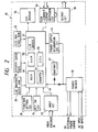
- the counter 20 has an input circuit 22 to which the encoder 18 can be connected, a key switch circuit 24, a function setting circuit 26, an LCD driving clock generating circuit 28, a system clock generating circuit 30, an LCD reference voltage generating circuit 32, and LCD display unit 34, a non-contact output inversion circuit 36, an output circuit 38, a power source circuit 40, a battery 42, serving as an auxiliary power source for supplying the electric power when the ordinary power source is interrupted, a power supply interruption detecting circuit 44, and a data processing circuit 46.
- the data processing circuit 46 has a ROM 48, a RAM 50, and LCD driver 52, a counter circuit 54, an a CPU 56.
- the output circuit 38 supplies a coincidence signal to a control circuit (not shown).
- a switching signal provided by an output inversion switch (not shown) is applied to the non-contact output inversion circuit 36.
- FIG. 3 shows the front panel of the counter 20.
- the LCD display 34, a teach mode key 58, a mode key 60, a shift key 62, and up key 64, a teach key 66, and a reset key 68 are provided on the front panel of counter 20.
- the LCD display unit 34 has mode displays 300, 302, and 304 displaying a number of stages of a preset value, and input and output modes.
- a "power on” display is indicated at 306.
- a control output display is indicated at 308.
- a count value display is indicated at 310 to display a current count value with zero suppression.
- a preset value display is indicated at 312 to display the contents of an operation mode when set.
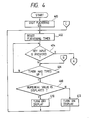
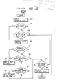
- FIGS. 4 and 5 are flow charts describing the operation of the embodiment of the invention.
- Step 400 a digit of a numerical value begins flickering, and then a flickering timer is reset in Step 402.
- Step 404 it is detected whether or not a key input is provided.
- Step 406 it is determined whether or not the flickering timer reset in step 402 has timed out. If the flickering timer has not yet timed out, Step 404 is repeated. Otherwise Step 308 is activated.
- step 408 detects whether or not a numerical value is being displayed. If “yes”, the display of the numerical value is stopped in Step 410; and if "no", the display of the numerical value is carried out again in Step 412. In each case, Step 402 is effected again, resetting the flickering timer. Thus, on the LCD display unit 34, the display of the numerical value at the designated place flickers for a predetermined period of about one second.
- Step 500 it is determined whether or not the operation key detected is the reset key 68. If “yes”, a reset operation is carried out. If “no”, in Step 502 it is next determined whether or not the operation key is the mode key 60. If “no”, in Step 504 it is determined whether or not the operation key is the shift key 62. If “yes” a shifting operation described below is performed. If “no”, it is determined in Step 506 whether or not the operation key is the up key 64. If it is determined that all these keys are not operated, Step 406 is carried out again. If either the shift or up key is operated, control is returned to Step 402 upon completion of the corresponding operation.
- Operation of the mode key 60 causes selecting the stage number for a preset value.
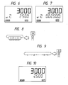
- FIG. 6. shows an example of a display when the operation causes setting a preset value at the second stage.
- the present count, "3000”, is displayed (Step 518), and a preset value "2500" is displayed being zero-suppressed.
- Step 520 When, under this condition, the shift key 62 or the up key 64 is operated (Step 520), a numerical value can be set (Step 522), so that the display of the least significant digit "0" of the preset value is flickered, as shown in FIG. 7.
- Step 508 The location of the flickering is shifted as shown in FIG. 8 each time the shift key 62 is operated (Step 508).
- the previously flickering digit is displayed continuously (Step 510).
- the display of the digit at the new flickering location is then forcibly stopped in Step 512, the Step 402 which initiates a flickering timer (FIG. 4) is carried out again.
- Step 514 the numerical value at the flickering location is incremented consecutively (Step 514), as shown in FIG. 9, the incremented digit at the flickering location is displayed at each time of pressing the up key 64 (Step 516).
- the place to be changed can be readily detected, and the set value (preset value) can be quickly and readily changed by operating the up key 64.
- the set value is registered (Step 526).
- the number of stages is one that is at the first stage, the number of stages of a preset value is not displayed as shown in FIG. 10.
- the above-described operation is applicable not only to a numerical value such as a preset value but also to other set parameters.
- a set value registering timer is started (Step 530) to run for a predetermined period of time.
- the set value is automatically registered.
- the specific feature of the numerical value setting device according to the invention resides in that, when the power supply is interrupted or restored during the numerical value setting operation or during the automatic registering latency time, the device is not already effected. That is, the device can achieve the numerical value setting operation and the set value registering operation satisfactorily, as described below.
- the CPU operating clock frequency is changed depending on whether or not the power supply is interrupted, because power consumption varies in proportion to the variations in the clock frequency.
- the clock frequency is about several MHz whereas it is about 100 KHz when the battery is employed on behalf of the ordinary power supply.
- the automatic registering latency time is previously set to 5 sec in the set value resistering timer by the manufacturer.
- clock pulses counted by the set value resistering timer When electrical power is supplied to the device, clock pulses counted by the set value resistering timer, have a clock period of 5 ms. Therefore, counting 1000 clock pulses reaches 5 sec.
- the clock pulses counted by the set value registering timer When the electric power supply to the device is interrupted, the clock pulses counted by the set value registering timer have a clock period of 60 ms. Thus, when the electric power supply to the device is interrupted, counting 83 clock pulses reaches 5 sec. It should be noted that when electric power is interrupted, the circuits of the device can be powered by battery 42.
- Step 525) the number of clock pulses, that is, the number of interruptions used for counting the resistering latency time, which is set in the set value registering timer when the electric power supply is interrupted, is calculated.
- the following arithmetic operation is carried out:
- Remaining time 5 sec. -[(the number of clock pulses counted during the electric power supply) x 5 ms] The calculation will result in 3 seconds (Step 527).
- the count value X that is, the number of clock pulses counted by the set value registering timer when the electric power supply to the device is interrupted is obtained as follows:
- the value x 50 is thus obtained and newly set in the set value registering timer.
- the 60 ms-period clock pulses are used when the electric power supply to the device is interrupted, e.g. after 2 seconds of maintained electric power, as in the present example.
- Step 532 the operation in Step 532 has ben accomplished.
- Step 524 when the up key operation or shift key operation is accomplished under the normal condition ("yes" in Step 524), the set value registering timer starts (Step 530), and at the end of a predetermined period of time (the automatic registering latency time), the set value is automatically registered (Step 526).
- the device is not affected thereby; that is, it can register the set value in the same manner at all times.
Landscapes
- Physics & Mathematics (AREA)
- General Physics & Mathematics (AREA)
- Measurement Of Predetermined Time Intervals (AREA)
- Electrophonic Musical Instruments (AREA)
- Feedback Control In General (AREA)
- Electric Clocks (AREA)
- Sub-Exchange Stations And Push- Button Telephones (AREA)
- Control Of Amplification And Gain Control (AREA)
- Pulse Circuits (AREA)
Applications Claiming Priority (2)
| Application Number | Priority Date | Filing Date | Title |
|---|---|---|---|
| JP63272460A JP2824908B2 (ja) | 1988-10-28 | 1988-10-28 | 数値設定装置 |
| JP272460/88 | 1988-10-28 |
Publications (3)
| Publication Number | Publication Date |
|---|---|
| EP0366495A2 true EP0366495A2 (fr) | 1990-05-02 |
| EP0366495A3 EP0366495A3 (fr) | 1992-01-22 |
| EP0366495B1 EP0366495B1 (fr) | 1994-09-07 |
Family
ID=17514224
Family Applications (1)
| Application Number | Title | Priority Date | Filing Date |
|---|---|---|---|
| EP89311133A Expired - Lifetime EP0366495B1 (fr) | 1988-10-28 | 1989-10-27 | Dispositif d'ajustage à une valeur numérique |
Country Status (7)
| Country | Link |
|---|---|
| US (1) | US5218579A (fr) |
| EP (1) | EP0366495B1 (fr) |
| JP (1) | JP2824908B2 (fr) |
| AT (1) | ATE111242T1 (fr) |
| DE (1) | DE68918044T2 (fr) |
| ES (1) | ES2063142T3 (fr) |
| HK (1) | HK148595A (fr) |
Family Cites Families (6)
| Publication number | Priority date | Publication date | Assignee | Title |
|---|---|---|---|---|
| JPS5389726A (en) * | 1977-01-19 | 1978-08-07 | Nippon Gakki Seizo Kk | Electronic musical instrument |
| DE3122037A1 (de) * | 1981-05-29 | 1983-01-05 | Siemens AG, 1000 Berlin und 8000 München | Elektronisches regelgeraet |
| DE3335219A1 (de) * | 1983-09-29 | 1985-04-11 | Gossen Gmbh, 8520 Erlangen | Digitaler mehrfach-regler |
| JPS61154316A (ja) * | 1984-12-27 | 1986-07-14 | Toshiba Corp | 位置検出器 |
| GB2188749A (en) * | 1986-01-07 | 1987-10-07 | Electric Design Limited | Programmable timer |
| JPH0685121B2 (ja) * | 1987-03-31 | 1994-10-26 | オムロン株式会社 | 制御装置 |
-
1988
- 1988-10-28 JP JP63272460A patent/JP2824908B2/ja not_active Expired - Fee Related
-
1989
- 1989-10-27 AT AT89311133T patent/ATE111242T1/de not_active IP Right Cessation
- 1989-10-27 EP EP89311133A patent/EP0366495B1/fr not_active Expired - Lifetime
- 1989-10-27 DE DE68918044T patent/DE68918044T2/de not_active Expired - Fee Related
- 1989-10-27 ES ES89311133T patent/ES2063142T3/es not_active Expired - Lifetime
- 1989-10-30 US US07/428,308 patent/US5218579A/en not_active Expired - Lifetime
-
1995
- 1995-09-14 HK HK148595A patent/HK148595A/en not_active IP Right Cessation
Also Published As
| Publication number | Publication date |
|---|---|
| DE68918044T2 (de) | 1995-03-02 |
| ES2063142T3 (es) | 1995-01-01 |
| HK148595A (en) | 1995-09-22 |
| US5218579A (en) | 1993-06-08 |
| EP0366495A3 (fr) | 1992-01-22 |
| JP2824908B2 (ja) | 1998-11-18 |
| ATE111242T1 (de) | 1994-09-15 |
| EP0366495B1 (fr) | 1994-09-07 |
| DE68918044D1 (de) | 1994-10-13 |
| JPH02119429A (ja) | 1990-05-07 |
Similar Documents
| Publication | Publication Date | Title |
|---|---|---|
| US6791599B1 (en) | Apparatus for driving liquid crystal shutter glasses and spatial transmission signal transmitting apparatus for liquid crystal shutter glasses | |
| US4945373A (en) | Display system for camera | |
| CA1134152A (fr) | Minuterie a affichage | |
| EP0657793A1 (fr) | Montre électronique corrigée par radio | |
| US5218579A (en) | Numerical value setting device | |
| US6002652A (en) | Pointer-type electronic clock | |
| EP0094174A2 (fr) | Dispositif de correction de vitesse pour l'utilisation dans un système de commande de vitesse | |
| US4588989A (en) | Supervisory device for wrong operation of varying quantity measuring apparatus | |
| US5003257A (en) | Digital speedometer displaying of measured object without flickering of least significant digit of displayed value | |
| JP2745579B2 (ja) | カウント装置 | |
| EP1133211A2 (fr) | Dispositif d'information avec haut-parleur | |
| JPH0628872Y2 (ja) | 接点入力情報送信装置 | |
| JP2701264B2 (ja) | 数値設定器 | |
| JPH02134020A (ja) | 数値設定装置 | |
| JPS5748449A (en) | Detecting method of operating position of limit switch detecting original point in numerically controlled machine tool | |
| JPS6243237B2 (fr) | ||
| KR20000006787A (ko) | 신호등의 주 제어기와는 별도로 신호등의 신호 변화만을인식하여 보행자와 운전자에 신호등 동작의 남은 시간을표시해주는 제어기 | |
| JPH028129B2 (fr) | ||
| KR920001341B1 (ko) | 교류전원 주파수 검출방법 | |
| JPH01137151A (ja) | 空気調和機 | |
| JPS6425166A (en) | Image forming device | |
| EP0401381A1 (fr) | Dispositif d'indication de donnees de derogation | |
| KR970001335B1 (ko) | 세탁기의 세탁량 표시/알람 장치 및 그 세탁 자동 제어방법 | |
| KR0125758B1 (ko) | 공기조화기의 제어방법 | |
| JPH0665896U (ja) | 製造機械、作業機械等の各種連続稼動機器に装備されるワンショットタイムカウンター |
Legal Events
| Date | Code | Title | Description |
|---|---|---|---|
| PUAI | Public reference made under article 153(3) epc to a published international application that has entered the european phase |
Free format text: ORIGINAL CODE: 0009012 |
|
| AK | Designated contracting states |
Kind code of ref document: A2 Designated state(s): AT BE CH DE ES FR GB GR IT LI LU NL SE |
|
| RAP1 | Party data changed (applicant data changed or rights of an application transferred) |
Owner name: OMRON CORPORATION |
|
| PUAL | Search report despatched |
Free format text: ORIGINAL CODE: 0009013 |
|
| AK | Designated contracting states |
Kind code of ref document: A3 Designated state(s): AT BE CH DE ES FR GB GR IT LI LU NL SE |
|
| 17P | Request for examination filed |
Effective date: 19920601 |
|
| 17Q | First examination report despatched |
Effective date: 19930115 |
|
| GRAA | (expected) grant |
Free format text: ORIGINAL CODE: 0009210 |
|
| AK | Designated contracting states |
Kind code of ref document: B1 Designated state(s): AT BE CH DE ES FR GB GR IT LI LU NL SE |
|
| PG25 | Lapsed in a contracting state [announced via postgrant information from national office to epo] |
Ref country code: IT Free format text: LAPSE BECAUSE OF FAILURE TO SUBMIT A TRANSLATION OF THE DESCRIPTION OR TO PAY THE FEE WITHIN THE PRE;WARNING: LAPSES OF ITALIAN PATENTS WITH EFFECTIVE DATE BEFORE 2007 MAY HAVE OCCURRED AT ANY TIME BEFORE 2007. THE CORRECT EFFECTIVE DATE MAY BE DIFFERENT FROM THE ONE RECORDED.SCRIBED TIME-LIMIT Effective date: 19940907 Ref country code: CH Effective date: 19940907 Ref country code: LI Effective date: 19940907 Ref country code: BE Effective date: 19940907 Ref country code: GR Free format text: LAPSE BECAUSE OF FAILURE TO SUBMIT A TRANSLATION OF THE DESCRIPTION OR TO PAY THE FEE WITHIN THE PRESCRIBED TIME-LIMIT Effective date: 19940907 Ref country code: AT Effective date: 19940907 |
|
| REF | Corresponds to: |
Ref document number: 111242 Country of ref document: AT Date of ref document: 19940915 Kind code of ref document: T |
|
| REF | Corresponds to: |
Ref document number: 68918044 Country of ref document: DE Date of ref document: 19941013 |
|
| PG25 | Lapsed in a contracting state [announced via postgrant information from national office to epo] |
Ref country code: LU Free format text: LAPSE BECAUSE OF NON-PAYMENT OF DUE FEES Effective date: 19941031 |
|
| PG25 | Lapsed in a contracting state [announced via postgrant information from national office to epo] |
Ref country code: SE Effective date: 19941207 |
|
| REG | Reference to a national code |
Ref country code: CH Ref legal event code: PL |
|
| ET | Fr: translation filed | ||
| REG | Reference to a national code |
Ref country code: ES Ref legal event code: FG2A Ref document number: 2063142 Country of ref document: ES Kind code of ref document: T3 |
|
| PLBE | No opposition filed within time limit |
Free format text: ORIGINAL CODE: 0009261 |
|
| STAA | Information on the status of an ep patent application or granted ep patent |
Free format text: STATUS: NO OPPOSITION FILED WITHIN TIME LIMIT |
|
| 26N | No opposition filed | ||
| PGFP | Annual fee paid to national office [announced via postgrant information from national office to epo] |
Ref country code: ES Payment date: 19981019 Year of fee payment: 10 |
|
| PGFP | Annual fee paid to national office [announced via postgrant information from national office to epo] |
Ref country code: NL Payment date: 19981028 Year of fee payment: 10 |
|
| REG | Reference to a national code |
Ref country code: GB Ref legal event code: 746 Effective date: 19990419 |
|
| PG25 | Lapsed in a contracting state [announced via postgrant information from national office to epo] |
Ref country code: ES Free format text: LAPSE BECAUSE OF NON-PAYMENT OF DUE FEES Effective date: 19991028 |
|
| PG25 | Lapsed in a contracting state [announced via postgrant information from national office to epo] |
Ref country code: NL Free format text: LAPSE BECAUSE OF NON-PAYMENT OF DUE FEES Effective date: 20000501 |
|
| NLV4 | Nl: lapsed or anulled due to non-payment of the annual fee |
Effective date: 20000501 |
|
| REG | Reference to a national code |
Ref country code: GB Ref legal event code: IF02 |
|
| REG | Reference to a national code |
Ref country code: ES Ref legal event code: FD2A Effective date: 20001113 |
|
| PGFP | Annual fee paid to national office [announced via postgrant information from national office to epo] |
Ref country code: DE Payment date: 20071031 Year of fee payment: 19 |
|
| PGFP | Annual fee paid to national office [announced via postgrant information from national office to epo] |
Ref country code: FR Payment date: 20071009 Year of fee payment: 19 Ref country code: GB Payment date: 20071024 Year of fee payment: 19 |
|
| GBPC | Gb: european patent ceased through non-payment of renewal fee |
Effective date: 20081027 |
|
| REG | Reference to a national code |
Ref country code: FR Ref legal event code: ST Effective date: 20090630 |
|
| PG25 | Lapsed in a contracting state [announced via postgrant information from national office to epo] |
Ref country code: DE Free format text: LAPSE BECAUSE OF NON-PAYMENT OF DUE FEES Effective date: 20090501 |
|
| PG25 | Lapsed in a contracting state [announced via postgrant information from national office to epo] |
Ref country code: FR Free format text: LAPSE BECAUSE OF NON-PAYMENT OF DUE FEES Effective date: 20081031 |
|
| PG25 | Lapsed in a contracting state [announced via postgrant information from national office to epo] |
Ref country code: GB Free format text: LAPSE BECAUSE OF NON-PAYMENT OF DUE FEES Effective date: 20081027 |