EP0366566B1 - Referenzelektroden - Google Patents
Referenzelektroden Download PDFInfo
- Publication number
- EP0366566B1 EP0366566B1 EP89402991A EP89402991A EP0366566B1 EP 0366566 B1 EP0366566 B1 EP 0366566B1 EP 89402991 A EP89402991 A EP 89402991A EP 89402991 A EP89402991 A EP 89402991A EP 0366566 B1 EP0366566 B1 EP 0366566B1
- Authority
- EP
- European Patent Office
- Prior art keywords
- reference electrode
- layer
- silver
- film
- salt
- Prior art date
- Legal status (The legal status is an assumption and is not a legal conclusion. Google has not performed a legal analysis and makes no representation as to the accuracy of the status listed.)
- Expired - Lifetime
Links
Images



Classifications
-
- G—PHYSICS
- G01—MEASURING; TESTING
- G01N—INVESTIGATING OR ANALYSING MATERIALS BY DETERMINING THEIR CHEMICAL OR PHYSICAL PROPERTIES
- G01N27/00—Investigating or analysing materials by the use of electric, electrochemical, or magnetic means
- G01N27/26—Investigating or analysing materials by the use of electric, electrochemical, or magnetic means by investigating electrochemical variables; by using electrolysis or electrophoresis
- G01N27/28—Electrolytic cell components
- G01N27/30—Electrodes, e.g. test electrodes; Half-cells
- G01N27/301—Reference electrodes
-
- G—PHYSICS
- G01—MEASURING; TESTING
- G01N—INVESTIGATING OR ANALYSING MATERIALS BY DETERMINING THEIR CHEMICAL OR PHYSICAL PROPERTIES
- G01N27/00—Investigating or analysing materials by the use of electric, electrochemical, or magnetic means
- G01N27/26—Investigating or analysing materials by the use of electric, electrochemical, or magnetic means by investigating electrochemical variables; by using electrolysis or electrophoresis
- G01N27/403—Cells and electrode assemblies
- G01N27/414—Ion-sensitive or chemical field-effect transistors, i.e. ISFETS or CHEMFETS
Definitions
- This invention relates to reference electrodes of solid type, which have a polymer film covering a surface of an electrically conductive substrate.
- an electrochemical reference electrode there is selected one, the output potential of which is not substantially changed electrochemically while it is in a liquid under test, which is subject to changes in the ion concentration, particularly hydrogen ion concentration.
- Such reference electrode are, typically, saturated calomel electrodes, silver/silver chloride electrodes and hydrogen electrodes.
- MOS FET metal oxide semiconductor field-effect transistor
- the prior art reference electrodes such as saturated calomel electrodes can be difficultly miniatuarized because there is a liquid junction between reference electrolytic solution and a vessel therefor.
- This invention has been developed in view of the above problems, and its object is to provide a reference electrode which can be readily miniatuarized, can provide a stable potential without being substantially influenced by the ion concentration and is excellent in stability and durability.
- a reference electrode comprising an electrically conductive substrate, a first lamination film provided on a surface of said substrate and including a silver halide layer and a hydrophobic resin layer and a second lamination film provided on a surface of said first lamination layer and including a hydrophobic resin layer and a salt layer, the composition of said salt layer being different from the composition of said silver halide layer.
- the second lamination film may be formed by alternately laminating silver halide layers and hydrophobic resin layers as well, at least one silver halide layer in the second lamination film containing a salt other than the silver halide, and/or at least one silver halide layer in the second lamination film being replaced with a layer of a salt other than the silver halide.
- the salt other than the silver halide are potassium chloride, sodium chloride, ammonium chloride, lithium chloride and other halide salts.
- the salt may be other than halide salts, e.g., sodium nitrate and sodium sulfate.
- a mixture film of a mixture consisting of a silver halide, a halide salt and hydrophobic resin may be formed on a surface of the second lamination film.
- a reference electrode comprising an electrically conductive substrate, a lamination layer provided on a surface of said substrate and formed by alternately laminating silver halide layers and hydrophobic resin layers and a mixture film consisting of a mixture of silver halide, a halide salt and a hydrophobic resin.
- the halide salt layers may contain a silver halide.
- the electrically conductive substrate is made of silver or consists of a silver layer formed on an insulator surface, and the silver halide is suitably a member of a group consisting of silver chloride, silver bromide, silver iodide and silver fluoride.
- the hydrophobic resin may be any resin having hydrophobicity, e.g., polyolefin, polystyrene, polyimide, polycarbonate, polymethyl-methacrylate (PMMA), polytetrafluoroethylene, polyvinyl fluoride, polyvinylidene fluoride and other fluorine resins. Polytetrafluoroethylene is particularly suitably used.
- a hydrophilic film, a gel film, or an ion-permeable film may suitably be formed on a surface of the lamination film or mixture film for improving the antithrombic separation of trapped matter and ions or passage of ions, particularly chlorine ions.
- These films may suitably be perfluoro ion-exchange films of polyvinyl chloride-polyethyleneglycol copolymer, styrene-hydroxyethylmethacrylate (HEMA), styrene-hydroxyethyl-methacrylate block polymer, polyurethane, polyvinyl alcohol, polyhydroxethyl-methacylate, polyacrylamide gel, nafion (trademark), etc.
- HEMA styrene-hydroxyethylmethacrylate
- styrene-hydroxyethyl-methacrylate block polymer polyurethane
- polyvinyl alcohol polyhydroxethyl-methacylate
- the halide salt layers and the like are formed by a vacuum deposition process, a sputtering process, an ion plating process, a cluster ion beam process, etc., while the hydrophobic resin layers are formed by a CVD (chemical vapor deposition) process, and ion plating process, a cluster ion beam process, a plasma polymerization process, a sputtering process, a photoresist process, etc.
- CVD chemical vapor deposition
- the lamination film may be formed on a surface of a gate insulation film of a field-effect transistor either directly or via a thin layer of silver.
- each halide layer has a role of the reference electrolyte and reference electrolyte chamber in the conventional reference electrode.
- this reference electrode permits determination of ion concentration by immersing it together with an ion electrode in an aqueous solution, to use it as electrode for reference potential generation in the ion concentration measurement, and measuring the potential difference between the reference electrode and ion electrode.
- the second lamination film contains a halide salt such as potassium chloride or sodium chloride as a thin film or as a component of a mixture
- a halide salt such as potassium chloride or sodium chloride
- dissociated chlorine ions are supplied through the hydrophobic resin layer to the neighborhood of silver halide layer. Therefore, silver ions and chloride ion can be held sufficiently inside the electrode. It is thus possible to effectively prevent silver ions from flowing out to the outside by preventing liquation of silver chloride which takes place with the lapse of time. This permits prevention of the deterioration of the characteristics of the reference electrode to obtain stabilization and life extension.
- the reference electrode according to the invention is solid as noted before, and can be readily miniatuarized. Further, it is difficultly influenced by the pH and chlorine ion concentration and can provide a constant potential, thus improving the stability and durability. Further, the lamination film can be formed under the room temperature condition with an atom beam sputtering apparatus being used. Thus, high dimensional accuracy of pattern formation can be obtained, and mass production is possible by performing the formation in a semiconductor manufacturing process. Further, since the intended function can be obtained with 1,000 angstroms or below of the thickness of the lamination film, the reference electrode may be utilized in a form integrated with a sensor in an ultramicro area of the order of microns.
- the reference electrode according to the invention is a solid electrode with a lamination film formed on an electrically conductive substrate or a gate insulation film of a field-effect transistor and comprising silver halide layers and hydrophobic resin layers, the inner liquid chamber and liquid junction that are necessary with the conventional electrode are unnecessary, so that it is possible to realize miniatuarization.
- this reference electrode is immersed in an aqueous solution, the hydrophobic resin layer swells. Since it is very thin (not thicker than 10 microns), water can migrate into the lamination film to cause dissociation of the silver halide. In other words, the lamination film itself can serve the role of an inner liquid.
- the hydrophobic layer can pass ions only very slightly and also has a laminar structure, and thus it can prevent flow-out of ions in it.
- This hydrophobic resin layer serves the role of the liquid junction.
- the reference electrode according to the invention can provide a stable potential like the conventional reference electrode having an inner liquid chamber.
- the silver halide layers are formed by the neutral beam sputtering process or a vapor deposition process, while the hydrophobic resin layers are formed by the neutral beam sputtering process.
- the electrode can be miniatuarized and also can be formed together with other ion sensors on a common chip, thus facilitating the manufacture of integrated sensors.
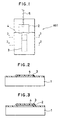
- An electrode base was prepared by forming, on the back surface of a saffire substrate 1 (having a face orientation of (1102) and a size of 15 mm by 15 mm by 0.4 mm) as shown in Fig. 1, a pattern of a thin layer 2 of chromium with a thickness of about 500 angstroms and then a pattern of a thin layer 3 of silver with a thickness of about 1,000 angstroms by a lift-off process using a DC sputtering apparatus (manufactured by Arnerba Inc.).
- the same electrode pattern as shown in Fig. 1 was also formed on a surface of an isotropic alumina substrate and on a surface of a glazed alumina substrate.
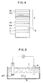
- a target of silver chloride and a target of a polytetrafluoroethylene resin (available under a trademark "Teflon") were alternately bombarded each 0 for every 30 minutes with a high-speed argon atom beam (1.15 to 1.2 mA in current level), provided by an atom beam sputtering apparatus by ionizing argon gas at 7 kV, then accelerating it and then neutralizing it again by providing an electron shower for causing particles flying out from the targets to be deposited on the surface of the electrode base, thus forming a lamination film 4 with a thickness of 300 to 500 angstroms as shown in schematic sectional profile in Fig. 4.
- the silver chloride layers 4a and polytetrafluoroethylene resin layers 4b in the lamination film 4 each had a thickness of 30 to 50 angstroms.
- a lead 5 was connected to the chromium thin layer 2 of the electrode base using an electrically conductive adhesive (available under a trade name "C-850-6" by Amicon Co., Ltd.).
- an electrically conductive adhesive available under a trade name "C-850-6" by Amicon Co., Ltd.
- a silicone resin PR 305, clear, Tore Silicone Co., Ltd.
- the reference electrode RE1 thus produced was held immersed in a 50-mM phosphate buffer liquid (with pH of 7.4) for 0,25, 45, 161 and 288 hours. Then, it was immersed together with a commercially available saturated sodium chloride calomel electrode (hereinafter referred to as SSCE) 9 in a phosphate buffer liquid 7 (with pH of 7.4, 50 mM) containing 0.154 M of sodium chloride, as shown in Fig. 5, and the output potential (Vout) of the electrode RE1 with respect to the SSEC 9 was measured while agitating the buffer liquid with an agitator 8.
- Fig. 7 shows the output potential of the electrode corresponding to the pH of the solution. It will be seen that this reference electrode provides a substantially constant potential irrespective of the pH. However, the electrodes using substrates other than the saffire substrate for the electrode base had weak durability, and their like was about 40 days.
- the reference electrode RE1 produced as above by using the saffire substrate was held immersed in a saturated sodium chloride aqueous solution for 45 days after the production, and during this time the chloride ion concentration dependency of the potential was evaluated.
- the same measurement method as in Experiment example 1 was adopted except for using a standard buffer solution with pH of 6.86 as liquid under test, varying the chloride ion concentration of the solution by dissolving sodium chloride in the solution and measuring the output potential with respect to the SSEC 9 at this time.
- Fig. 8 shows the output potential of the electrode corresponding to the chlorine ion concentration in the solution.
- the reference electrode RE1 provides a substantially constant potential irrespective of the chlorine ion concentration.
- Characteristics of the electrode were also examined after preserving the electrode in the solution noted above for 100 days. It was found that the electrode is not influenced by the pH so long as the pH is in a range of 4 to 9.2, and also no potential change was recognized in a chlorine ion concentration range of 0 to 1 M.
- a lamination film 4 including a silver chloride layer and a polytetrafluoroethylene resin layer was formed by the same method as in Experiment example 1.
- the lamination film 4 had a thickness of about 700 angstroms, and it was formed by lamination of 10 layers.
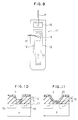
- a pH-ISFET electrode having an insulation film structure of a 1,000-angstrom silicon oxide film 13/ a 1,500-angstrom nitride film 14 was used, and leads 17 were connected in advance to source and drain regions 15 and 16.
- Fig. 10 shows a sectional structure taken along line 10-10 in Fig. 9.
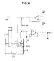
- the reference electrode RE2 was held immersed in a phosphate buffer solution 19 in the measuring apparatus shown in Fig. 6, and the output potential (Vout) of the electrode RE2 with respect to the SSEC 21 was measured while agitating the phosphate buffer solution 19 with an agitator 20 for examining the pH dependency and chlorine ion concentration dependency of the output potential.
- the electrode provided a constant potential within experimental errors ( ⁇ 1 mV) in a pH range of 1 to 10, showing substantial freedom of the electrode from the dependency on pH and chlorine ion concentration.
- the electrode can be utilized sufficiently as a reference electrode for a semiconductor sensor so long as a shift of the output voltage is made.
- a thin film 22 of silver (with a thickness of 50 to 300 angstroms) was formed by vacuum deposition on a surface of a gate insulation film 12 of a ISFET, as shown in Fig. 11, in the same manner as for Reference Electrode 2. Then a lamination film 4 (with a thickness of 700 angstroms) consisting of a silver chloride layer and a polytetrafluoroethylene layer was formed on the entire surface of the silver chloride film 22 in the same manner as for Reference Electrode 1.
- an electrode base was prepared by forming, on the back surface of a saffire substrate 31 (having a face orientation of (1 1 02) and a size of 15 mm by 15 mm by 0.4 mm), a pattern of a thin layer 32 of chronium with a thickness of about 500 angstroms and then a pattern of a thin layer 33 of silver with a thickness of about 1,000 angstroms by a lift-off process using a DC sputtering apparatus.
- the same electrode pattern as shown in Fig. 12 was also formed on a surface of an isotropic alumina substrate and also on a surface of a glazed alumina substrate.
- targets of silver chloride, polytetrafluoroethylene resin and potassium chloride were alternately bombarded with a high-speed argon atom beam (1.2 mA in current level, incidence angle of 30 to 45 degrees), provided by an atom beam sputtering apparatus by ionizing argon gas at 7 kV, then accelerating it and then neutralizing it again by providing an electron shower for causing particles flying out from the targets to be deposited on the surface of the electrode base, thus forming a lamination film 34 with a thickness of about 2,500 angstroms.
- the silver chloride layers 34a, polytetrafluoroethylene resin layers 34b and potassium chloride layers 34c of the lamination film 34 each had a thickness of about 50 angstroms.
- a lead 36 is connected to the silver thin layer 33 of the electrode base using an electrically conductive adhesive 35 (C-850-6, Amicon Inc.). Thereafter, an insulating film 37 consisting of an epoxy resin layer 37a and a Teflon coat enamel film 37b was provided to conceal the connected portion of the lead 36 and chromium and silver thin layers 32 and 33, thus completing the reference electrode 38 (Fig. 12).
- the reference electrode 38 thus produced was held immersed together with SSEC in phosphate buffer solutions with chlorine ion concentrations of 0.001, 0.1 and 1.0 M, and the output potential (Vout) of the electrode 38 with respect to the SSCE was measured while agitating the solution with an agitator.
- Fig. 15 shows the output potential of the electrode corresponding to the chlorine ion concentration of the solution.
- the reference electrode of this embodiment provides a substantially constant potential irrespective of the chlorine ion concentration.
- the characteristics of the electrode were examined after preserving the electrode in the solution noted above for 100 days. It was found that the output potential is free from the influence of the pH in a range of 4 to 9.2 and also is free from influence by chlorine ion concentration in a range of 0 to 1 M.
- a lamination film with a thickness of 500 angstroms was formed by alternately laminating silver chloride layers, polytetrafluoroethylene layers and potassium chloride layers by the method as in Embodiment 1, and then lead is connected to complete a reference electrode.
- a lamination film with a thickness of 50 angstroms was formed by alternately laminating silver chloride layers, polytetrafluoroethylene layers and potassium chloride layers in the manner as in Embodiment 2.
- the output potentials of the reference electrodes in the embodiments 2 and 3 with respect to the SSCE were measured in the manner as in Experiment example 5.
- Fig. 15 shows the result.
- the reference electrode in Embodiment 2 provided a substantially constant potential irrespective of chlorine ion concentration.
- the reference electrode in Embodiment 3, which had a small film thickness, could not prevent flow-out of chlorine ions, and therefore showed a slight slope of the plot of the output potential versus chlorine ion concentration.
- a thin film of chromium with a thickness of about 100 angstroms was formed on a surface of a saffire substrate (having a face orientation on a (1002) using a DC sputtering apparatus. Then, a silver chloride layer with a thickness of 300 angstroms and containing 0.1 to 10 % of sodium chloride and then a thin layer of silver with a thickness of about 500 angstroms were formed on a surface of the silver thin layer using a vacuum deposition apparatus.
- a polytetrafluoroethylene thin film with a thickness of about 100 angstroms was formed to cover the silver chloride layer by causing bombardment of a polytetrafluoroethylene target by a neutral argon beam using a neutral atom sputtering apparatus (Embodiment 4).
- the electrodes produced in Embodiments 4 to 6 were each held immersed as function electrode together with a SSCE in a sample solution and their electromotive force response was measured using an electrometer (manufactured by Advan Test Co., Ltd.). More specifically, the pH dependency was examined using standard buffer solutions with pH of 4.01, 6.86 and 9.18. The reference electrodes of Embodiments 4 to 6 were all free from influence of the pH. Further, the chlorine ion concentration dependency was examined by varying the chlorine ion concentration to 0.01, 0.1 and 1 M by adding sodium chloride while holding a constant pH (of 6.86). The electrodes of Embodiments 4 to 6 all came to show a potential close to a theoretical level (-40 mW with respect to SSCE) in about one hour from the instant when they were immersed in solution.
- a silver layer with a thickness of 500 angstroms was formed on a sapphire substrate in the manner as shown in Embodiment 7, and then a silver chloride layer with a thickness of about 300 angstroms was formed using a vacuum deposition apparatus.
- a solution obtained by dissolving 0.5 to 1 % of polymethyl-methacrylate (PMMA, with a molecular weight of 10 6 to 10 7 ) in a methylisobuthylketone (MIBK) as solvent was coated on the silver chloride layer using a spin coating apparatus and under conditions of 1,000 rpm and 30 seconds.
- the coating was then dried at 110 °C for 30 minutes and then thermally processed at 170 °C for 10 minutes, thus forming a polymethylmethacrylate film with a thickness of 500 to 1,000 angstroms.
- a silver chloride layer containing 1 % of sodium chloride was formed using a vacuum deposition apparatus to cover the polymethyl-methacrylate film.
- a polymethyl-methacrylate film with a thickness of 500 angstroms was formed in the same method as described above.
- the silver chloride layer containing sodium chloride and polymethyl-methacrylate layer were laminatingly formed alternately ten times.
- a lead end portion was masked as connected portion with a tape of polyimide (available under a trademark "Capton"), and after formation of the lamination film the tape was peeled off, and the lead (i.e., thin copper wire) was bonded using a silver paste.
- the entire base was covered for insulation with an epoxy resin adhesive and a Teflon coat enamel film such as to expose a central portion with about 2 mm by 2 mm of the polymethyl-methacrylate film.
- a reference electrode was produced in the same manner as in Embodiment 7 except for that "Fluororesist” (a trademark by Daikin Kogyo Co., Ltd.) was used in lieu of polymethylmethacrylate.
- "Fluororesist” contains a resin obtained by grafting a fluorine-based polymer in polymethyl-methacrylate.
- a reference electrode was produced in the same manner as in Embodiment 7 except for that a polyimide-based photoresist (for instance "Photoneese", a trademark by Tore Co., Ltd.) in lieu of polymethyl-methacrylate.
- a polyimide-based photoresist for instance "Photoneese", a trademark by Tore Co., Ltd.
- prebaking was subsequently done at 110 °C for 20 minutes, and then UV ultraviolet exposure was done, and postbaking was done several times at 180 to 400°C.
- a lamination film consisting of a silver chloride layer and a polytetrafluoroethylene resin layer was formed on a surface of a gate insulation film of a MOS ISFET in the manner as for Reference Electrodes 7 to 12.
- gate insulation film a silicon wafer with an insulating film consisting of a silicon oxide layer (1,000 angstroms thick) and a silicon nitride layer (1,500 angstroms thick).
- a silver/silver chloride layer and a silver chloride layer were deposition formed on the ISFET substrate surface, and an electrode pattern was formed on and in the neighborhood of the gate insulation film by a lift-off process.
- the polytetrafluoroethylene resin layer was formed only on a gate insulation section using a metal mask and a neutral argon atom beam sputtering apparatus, while forming the silver chloride layer using a vacuum deposition apparatus.
- the polyimide-based photoresist was spin-coated to a thickness of 500 angstroms and then exposed and developed using a photomask to selectively leave a resist film on the gate insulation film only. Subsequently, postbaking was done at about 400 °C, and a silver chloride layer was deposited using a meral mask.
- Lamination film was formed in this way, and then a photoresist film was formed over the entire surface, followed by UV exposure leaving source and drain electrode contact sections and postbaking at 180 to 400 °C for insulation.
- Embodiments 7 to 9 were tested to examine the pH and chlorine ion concentration dependencies of the output potential using the same method as in Experiment example 8. It was found that there was substantially no influence by pH in a pH range of 2 to 10 and also influence by the chlorine ion concentration was not substantial. Further, after immersion in solution values near the theoretical value (-40 mV, with respect to SSCE) could be obtained in 30 minutes to 5 hours.
- the FET electrodes produced as Reference Electrodes 13 and 14 were each connected to an ISFET driver, and their output potential with respect to SSCE was measured in the manner as in Experiment example 8. It was found that the output voltage was stable and independent of the pH and chlorine ion concentrations.
Landscapes
- Chemical & Material Sciences (AREA)
- Life Sciences & Earth Sciences (AREA)
- Health & Medical Sciences (AREA)
- Physics & Mathematics (AREA)
- Chemical Kinetics & Catalysis (AREA)
- Electrochemistry (AREA)
- Molecular Biology (AREA)
- Analytical Chemistry (AREA)
- Biochemistry (AREA)
- General Health & Medical Sciences (AREA)
- General Physics & Mathematics (AREA)
- Immunology (AREA)
- Pathology (AREA)
- Investigating Or Analyzing Materials By The Use Of Electric Means (AREA)
Claims (12)
- Referenzelektrode, umfassend ein elektrisch leitendes Substrat, einen ersten Laminatfilm, der auf einer Oberfläche des Substrats bereitgestellt ist und eine Silberhalogenidschicht sowie eine hydrophobe Harzschicht einschließt, und einen zweiten Laminatfilm, der auf einer Oberfläche des ersten Laminatfilms bereitgestellt ist und eine hydrophobe Harzschicht sowie eine Salzschicht einschließt, wobei die Zusammensetzung der Salzschicht von der Zusammensetzung der Silberhalogenidschicht verschieden ist.
- Referenzelektrode nach Anspruch 1, wobei der zweite Laminatfilm durch abwechselnde Laminierung von Silberhalogenidschichten und hydrophoben Harzschichten gebildet ist und mindestens eine Silberhalogenidschicht im zweiten Laminatfilm ein anderes Salz als Silberhalogenid enthält.
- Referenzelektrode nach Anspruch 1, wobei der zweite Laminatfilm durch abwechselnde Laminierung von Silberhalogenidschichten und hydrophoben Harzschichten gebildet ist und mindestens eine Silberhalogenidschicht im zweiten Laminatfilm durch ein von Silberhalogenid verschiedenes Salz ersetzt ist.
- Referenzelektrode nach einem der Ansprüche 2 und 3, wobei das Salz ein Halogenidsalz ist.
- Referenzelektrode nach einem der Ansprüche 2 und 3, wobei das Salz ein von irgendwelchen Halogenidsalzen, verschiedenes Salz ist.
- Referenzelektrode nach einem der vorhergehenden Ansprüche, wobei die Salzschicht Kaliumchlorid, Natriumchlorid oder Lithiumchlorid umfaßt.
- Referenzelektrode nach einem der vorhergehenden Ansprüche, wobei ein aus einem Gemisch aus Silberhalogenid, Halogenidsalz und hydrophobem Harz bestehender Mischfilm auf einer Oberfläche des zweiten Laminatfilms gebildet ist.
- Referenzelektrode, umfassend ein elektrisch leitendes Substrat, eine Laminatschicht, die auf einer Oberfläche des Substrats bereitgestellt ist und durch abwechselnde Laminierung von Silberhalogenidschichten und hydrophoben Harzschichten gebildet ist, sowie einen aus einem Gemisch aus Silberhalogenid, Halogenidsalz und hydrophobem Harz bestehenden Mischfilm.
- Referenzelektrode nach einem der Ansprüche 1 bis 8, wobei das elektrisch leitende Substrat aus Silber gemacht oder ein durch Bildung einer Silberschicht auf einer Oberfläche eines Isolators erhaltenes Substrat ist.
- Referenzelektrode nach einem der Ansprüche 1 bis 9, umfassend eine Silberhalogenidschicht aus einem Element einer aus Silberchlorid, Silberbromid, Silberiodid und Silberfluorid bestehenden Gruppe.
- Referenzelektrode, unfassend einen Laminatfilm gemäß einem, der Ansprüche 1 bis 8 und 10, wobei der Laminatfilm, auf einer Oberfläche eines Gate-Isolierfilms eines Feldeffekttransistors gebildet ist.
- Referenzelektrode, umfassend einen Laminatfilm gemäß einem der Ansprüche 1 bis 8 und 10, wobei der Laminatfilm über eine Dünnschicht aus Silber auf einer Oberfläche eines Gate-Isolierfilms eines Feldeffekttransistors gebildet ist.
Applications Claiming Priority (6)
| Application Number | Priority Date | Filing Date | Title |
|---|---|---|---|
| JP27178488 | 1988-10-27 | ||
| JP271784/88 | 1988-10-27 | ||
| JP28464/89 | 1989-02-06 | ||
| JP1028464A JP2969520B2 (ja) | 1989-02-06 | 1989-02-06 | 基準電極 |
| JP84551/89 | 1989-04-03 | ||
| JP1084551A JPH02193055A (ja) | 1988-10-27 | 1989-04-03 | 基準電極 |
Publications (3)
| Publication Number | Publication Date |
|---|---|
| EP0366566A2 EP0366566A2 (de) | 1990-05-02 |
| EP0366566A3 EP0366566A3 (de) | 1990-09-19 |
| EP0366566B1 true EP0366566B1 (de) | 1998-06-03 |
Family
ID=27286213
Family Applications (1)
| Application Number | Title | Priority Date | Filing Date |
|---|---|---|---|
| EP89402991A Expired - Lifetime EP0366566B1 (de) | 1988-10-27 | 1989-10-27 | Referenzelektroden |
Country Status (4)
| Country | Link |
|---|---|
| US (1) | US5066383A (de) |
| EP (1) | EP0366566B1 (de) |
| DE (1) | DE68928691T2 (de) |
| DK (1) | DK532589A (de) |
Families Citing this family (16)
| Publication number | Priority date | Publication date | Assignee | Title |
|---|---|---|---|---|
| EP0393188A4 (en) * | 1987-11-24 | 1991-01-02 | Terumo Kabushiki Kaisha | Reference electrode |
| DE59106341D1 (de) * | 1990-05-02 | 1995-10-05 | Pacesetter Ab | Silberchlorid-Bezugselektrode. |
| DE4017905A1 (de) * | 1990-06-02 | 1991-12-05 | Basf Ag | Referenzelektrode fuer chemische sensoren |
| US5185278A (en) * | 1990-10-22 | 1993-02-09 | Motorola, Inc. | Method of making self-aligned gate providing improved breakdown voltage |
| US5470453A (en) * | 1991-05-29 | 1995-11-28 | Mettler-Toledo Ag | Reference electrode with ion barrier for electrochemical measuring systems |
| JP2741511B2 (ja) * | 1991-07-10 | 1998-04-22 | 日本特殊陶業株式会社 | 基準電極 |
| US5384031A (en) * | 1992-04-29 | 1995-01-24 | Diametrics Medical, Inc. | Reference electrode |
| DE19534925C2 (de) * | 1995-09-20 | 2001-05-17 | Kurt Schwabe Inst Fuer Mes Und | Bezugselektrode für elektrochemische Messungen und Verfahren zu ihrer Herstellung |
| DE19748052A1 (de) * | 1997-10-30 | 1999-05-06 | Dieter Haaf | Brückenkörper für eine Elektrode |
| JP2001004581A (ja) * | 1999-06-24 | 2001-01-12 | Sentan Kagaku Gijutsu Incubation Center:Kk | 微小参照電極 |
| US20050241959A1 (en) * | 2004-04-30 | 2005-11-03 | Kenneth Ward | Chemical-sensing devices |
| US7373195B2 (en) | 2004-07-30 | 2008-05-13 | Medtronic, Inc. | Ion sensor for long term use in complex medium |
| KR101137736B1 (ko) * | 2004-09-30 | 2012-04-24 | 각코호진 와세다다이가쿠 | 반도체 센싱용 전계 효과형 트랜지스터, 반도체 센싱디바이스, 반도체 센서 칩 및 반도체 센싱 장치 |
| JP4857820B2 (ja) * | 2006-03-03 | 2012-01-18 | 学校法人早稲田大学 | Dnaセンシング方法 |
| FR2986867B1 (fr) * | 2012-02-14 | 2015-05-22 | Renault Sas | Electrode de reference d'un dispositif de stockage d'energie electrique |
| US11959870B2 (en) * | 2022-01-05 | 2024-04-16 | Hach Company | Differential probe with low-slope component |
Family Cites Families (19)
| Publication number | Priority date | Publication date | Assignee | Title |
|---|---|---|---|---|
| US3926764A (en) * | 1971-05-19 | 1975-12-16 | Radiometer As | Electrode for potentiometric measurements |
| GB1437091A (en) * | 1972-10-02 | 1976-05-26 | Radiometer As | Calcium electrode and membrane and composition for use therein |
| US3856649A (en) * | 1973-03-16 | 1974-12-24 | Miles Lab | Solid state electrode |
| US3957612A (en) * | 1974-07-24 | 1976-05-18 | General Electric Company | In vivo specific ion sensor |
| US3957613A (en) * | 1974-11-01 | 1976-05-18 | General Electric Company | Miniature probe having multifunctional electrodes for sensing ions and gases |
| US4280889A (en) * | 1976-03-11 | 1981-07-28 | Honeywell Inc. | Solid state ion responsive and reference electrodes |
| US4053381A (en) * | 1976-05-19 | 1977-10-11 | Eastman Kodak Company | Device for determining ionic activity of components of liquid drops |
| US4214968A (en) * | 1978-04-05 | 1980-07-29 | Eastman Kodak Company | Ion-selective electrode |
| JPS5924242A (ja) * | 1982-08-02 | 1984-02-07 | Terumo Corp | 基準電極 |
| GB2175400B (en) * | 1984-10-31 | 1989-07-19 | Unilever Plc | Apparatus for use in electrical,e.g.electrochemical,measurement procedures,and its production and use,and composite assemblies incorporating the apparatus |
| KR900008847B1 (ko) * | 1985-05-27 | 1990-11-30 | 테루모가부시끼가이샤 | 이온센서 및 그 제조방법 |
| DK626986A (da) * | 1985-12-25 | 1987-06-26 | Terumo Corp | Ionsensor |
| DE3687123T2 (de) * | 1986-01-24 | 1993-05-13 | Terumo Corp | Ionenempfindlicher fet-fuehler. |
| JPS62180263A (ja) * | 1986-02-04 | 1987-08-07 | Terumo Corp | 酸素センサ− |
| US4871442A (en) * | 1986-05-01 | 1989-10-03 | Terumo Corporation | Ion sensor |
| GB2190399A (en) * | 1986-05-02 | 1987-11-18 | Nat Res Dev | Multi-metal electrode |
| JPS62277547A (ja) * | 1986-05-26 | 1987-12-02 | Terumo Corp | ガスセンサ− |
| JPS636451A (ja) * | 1986-06-27 | 1988-01-12 | Terumo Corp | 酵素センサ |
| EP0393188A4 (en) * | 1987-11-24 | 1991-01-02 | Terumo Kabushiki Kaisha | Reference electrode |
-
1989
- 1989-10-26 US US07/426,713 patent/US5066383A/en not_active Expired - Lifetime
- 1989-10-26 DK DK532589A patent/DK532589A/da not_active Application Discontinuation
- 1989-10-27 EP EP89402991A patent/EP0366566B1/de not_active Expired - Lifetime
- 1989-10-27 DE DE68928691T patent/DE68928691T2/de not_active Expired - Fee Related
Non-Patent Citations (1)
| Title |
|---|
| PATENT ABSTRACTS OF JAPAN Vol 12 No 388 (P-771)(2723) 17th October 1988 & JP-A-6 313 1056 * |
Also Published As
| Publication number | Publication date |
|---|---|
| EP0366566A2 (de) | 1990-05-02 |
| DK532589D0 (da) | 1989-10-26 |
| DE68928691T2 (de) | 1998-10-15 |
| EP0366566A3 (de) | 1990-09-19 |
| US5066383A (en) | 1991-11-19 |
| DE68928691D1 (de) | 1998-07-09 |
| DK532589A (da) | 1990-04-30 |
Similar Documents
| Publication | Publication Date | Title |
|---|---|---|
| EP0366566B1 (de) | Referenzelektroden | |
| US4062750A (en) | Thin film electrochemical electrode and cell | |
| US6419809B1 (en) | Miniature reference electrode | |
| US5200053A (en) | Reference electrode | |
| US5213675A (en) | Reference electrode, ion sensor and method of manufacturing the same | |
| EP0673506B1 (de) | Referenzelektrode | |
| US20020157949A1 (en) | Field-effect transistor | |
| Li et al. | Elimination of neutral species interference at the ion-sensitive membrane/semiconductor device interface | |
| DK159861B (da) | Referenceelektrode med inaktiv polymermembran og fremgangsmaade til fremstilling heraf | |
| JPH02268265A (ja) | 電気化学測定用微細孔電極セル及びその製造方法 | |
| JPH09292361A (ja) | 参照電極の製造方法 | |
| GB2163457A (en) | Producing a fluoride sensitive membrane | |
| JPH0245147B2 (de) | ||
| Iken et al. | Development of a Combined pH‐and Redox‐Sensitive Bi‐Electrode Glass Thin‐Film Sensor | |
| JPS58167951A (ja) | 塩素イオンセンサ | |
| JP2577045B2 (ja) | 電気化学測定用微小電極セルおよびその製造方法 | |
| JP2969520B2 (ja) | 基準電極 | |
| JP2007508547A (ja) | ソリッドステート参照電極 | |
| JPH0219757A (ja) | 電気化学測定用微小電極セルおよびその製造方法 | |
| JPH02140655A (ja) | 電気化学的検出器およびその製造方法 | |
| JP3388942B2 (ja) | 固体膜型イオンセンサおよびその安定化方法 | |
| Goryll et al. | Integrated sensor design using ion channels inserted into lipid bilayer membranes | |
| JPH03221857A (ja) | 電気化学測定用微小電極セル | |
| JPS61195345A (ja) | イオンセンサの製造方法 | |
| Ho et al. | Sodium and potassium ion sensing properties of EIS and ISFET structures with fluorinated hafnium oxide sensing film |
Legal Events
| Date | Code | Title | Description |
|---|---|---|---|
| PUAI | Public reference made under article 153(3) epc to a published international application that has entered the european phase |
Free format text: ORIGINAL CODE: 0009012 |
|
| 17P | Request for examination filed |
Effective date: 19891102 |
|
| AK | Designated contracting states |
Kind code of ref document: A2 Designated state(s): BE DE FR GB IT NL SE |
|
| PUAL | Search report despatched |
Free format text: ORIGINAL CODE: 0009013 |
|
| AK | Designated contracting states |
Kind code of ref document: A3 Designated state(s): BE DE FR GB IT NL SE |
|
| 17Q | First examination report despatched |
Effective date: 19931126 |
|
| GRAG | Despatch of communication of intention to grant |
Free format text: ORIGINAL CODE: EPIDOS AGRA |
|
| GRAG | Despatch of communication of intention to grant |
Free format text: ORIGINAL CODE: EPIDOS AGRA |
|
| GRAH | Despatch of communication of intention to grant a patent |
Free format text: ORIGINAL CODE: EPIDOS IGRA |
|
| GRAH | Despatch of communication of intention to grant a patent |
Free format text: ORIGINAL CODE: EPIDOS IGRA |
|
| GRAA | (expected) grant |
Free format text: ORIGINAL CODE: 0009210 |
|
| AK | Designated contracting states |
Kind code of ref document: B1 Designated state(s): BE DE FR GB IT NL SE |
|
| PG25 | Lapsed in a contracting state [announced via postgrant information from national office to epo] |
Ref country code: IT Free format text: LAPSE BECAUSE OF FAILURE TO SUBMIT A TRANSLATION OF THE DESCRIPTION OR TO PAY THE FEE WITHIN THE PRE;WARNING: LAPSES OF ITALIAN PATENTS WITH EFFECTIVE DATE BEFORE 2007 MAY HAVE OCCURRED AT ANY TIME BEFORE 2007. THE CORRECT EFFECTIVE DATE MAY BE DIFFERENT FROM THE ONE RECORDED.SCRIBED TIME-LIMIT Effective date: 19980603 Ref country code: NL Free format text: LAPSE BECAUSE OF FAILURE TO SUBMIT A TRANSLATION OF THE DESCRIPTION OR TO PAY THE FEE WITHIN THE PRESCRIBED TIME-LIMIT Effective date: 19980603 Ref country code: BE Free format text: LAPSE BECAUSE OF FAILURE TO SUBMIT A TRANSLATION OF THE DESCRIPTION OR TO PAY THE FEE WITHIN THE PRESCRIBED TIME-LIMIT Effective date: 19980603 Ref country code: FR Free format text: LAPSE BECAUSE OF FAILURE TO SUBMIT A TRANSLATION OF THE DESCRIPTION OR TO PAY THE FEE WITHIN THE PRESCRIBED TIME-LIMIT Effective date: 19980603 |
|
| REF | Corresponds to: |
Ref document number: 68928691 Country of ref document: DE Date of ref document: 19980709 |
|
| PG25 | Lapsed in a contracting state [announced via postgrant information from national office to epo] |
Ref country code: SE Free format text: LAPSE BECAUSE OF FAILURE TO SUBMIT A TRANSLATION OF THE DESCRIPTION OR TO PAY THE FEE WITHIN THE PRESCRIBED TIME-LIMIT Effective date: 19980903 |
|
| EN | Fr: translation not filed | ||
| NLV1 | Nl: lapsed or annulled due to failure to fulfill the requirements of art. 29p and 29m of the patents act | ||
| PLBE | No opposition filed within time limit |
Free format text: ORIGINAL CODE: 0009261 |
|
| STAA | Information on the status of an ep patent application or granted ep patent |
Free format text: STATUS: NO OPPOSITION FILED WITHIN TIME LIMIT |
|
| 26N | No opposition filed | ||
| REG | Reference to a national code |
Ref country code: GB Ref legal event code: IF02 |
|
| PGFP | Annual fee paid to national office [announced via postgrant information from national office to epo] |
Ref country code: DE Payment date: 20021031 Year of fee payment: 14 |
|
| PGFP | Annual fee paid to national office [announced via postgrant information from national office to epo] |
Ref country code: GB Payment date: 20031022 Year of fee payment: 15 |
|
| PG25 | Lapsed in a contracting state [announced via postgrant information from national office to epo] |
Ref country code: DE Free format text: LAPSE BECAUSE OF NON-PAYMENT OF DUE FEES Effective date: 20040501 |
|
| PG25 | Lapsed in a contracting state [announced via postgrant information from national office to epo] |
Ref country code: GB Free format text: LAPSE BECAUSE OF NON-PAYMENT OF DUE FEES Effective date: 20041027 |
|
| GBPC | Gb: european patent ceased through non-payment of renewal fee |
Effective date: 20041027 |