EP0366916A2 - Halbleiteranordnung mit kurzgeschlossener Anode und Verfahren zu deren Herstellung - Google Patents
Halbleiteranordnung mit kurzgeschlossener Anode und Verfahren zu deren Herstellung Download PDFInfo
- Publication number
- EP0366916A2 EP0366916A2 EP89117033A EP89117033A EP0366916A2 EP 0366916 A2 EP0366916 A2 EP 0366916A2 EP 89117033 A EP89117033 A EP 89117033A EP 89117033 A EP89117033 A EP 89117033A EP 0366916 A2 EP0366916 A2 EP 0366916A2
- Authority
- EP
- European Patent Office
- Prior art keywords
- layer
- conductivity type
- substrate
- forming
- type
- Prior art date
- Legal status (The legal status is an assumption and is not a legal conclusion. Google has not performed a legal analysis and makes no representation as to the accuracy of the status listed.)
- Granted
Links
- 239000004065 semiconductor Substances 0.000 title claims abstract description 31
- 238000000034 method Methods 0.000 title claims description 10
- 239000000758 substrate Substances 0.000 claims abstract description 44
- 238000009792 diffusion process Methods 0.000 claims description 17
- 238000004519 manufacturing process Methods 0.000 claims description 16
- 239000012535 impurity Substances 0.000 claims description 12
- 230000015572 biosynthetic process Effects 0.000 claims description 3
- 238000000151 deposition Methods 0.000 claims description 3
- 229910052751 metal Inorganic materials 0.000 description 5
- 239000002184 metal Substances 0.000 description 5
- 239000008188 pellet Substances 0.000 description 5
- XUIMIQQOPSSXEZ-UHFFFAOYSA-N Silicon Chemical compound [Si] XUIMIQQOPSSXEZ-UHFFFAOYSA-N 0.000 description 4
- 230000004048 modification Effects 0.000 description 4
- 238000012986 modification Methods 0.000 description 4
- 238000000059 patterning Methods 0.000 description 4
- 238000007796 conventional method Methods 0.000 description 3
- 229910052710 silicon Inorganic materials 0.000 description 3
- 239000010703 silicon Substances 0.000 description 3
- 229910000679 solder Inorganic materials 0.000 description 3
- VYPSYNLAJGMNEJ-UHFFFAOYSA-N Silicium dioxide Chemical compound O=[Si]=O VYPSYNLAJGMNEJ-UHFFFAOYSA-N 0.000 description 2
- 230000008901 benefit Effects 0.000 description 2
- 230000003247 decreasing effect Effects 0.000 description 2
- 230000008020 evaporation Effects 0.000 description 2
- 238000001704 evaporation Methods 0.000 description 2
- 238000002161 passivation Methods 0.000 description 2
- 230000002093 peripheral effect Effects 0.000 description 2
- 229920002050 silicone resin Polymers 0.000 description 2
- 239000004809 Teflon Substances 0.000 description 1
- 229920006362 Teflon® Polymers 0.000 description 1
- 229910052782 aluminium Inorganic materials 0.000 description 1
- XAGFODPZIPBFFR-UHFFFAOYSA-N aluminium Chemical compound [Al] XAGFODPZIPBFFR-UHFFFAOYSA-N 0.000 description 1
- 230000003321 amplification Effects 0.000 description 1
- 238000005219 brazing Methods 0.000 description 1
- 230000015556 catabolic process Effects 0.000 description 1
- 229910010293 ceramic material Inorganic materials 0.000 description 1
- 229910017052 cobalt Inorganic materials 0.000 description 1
- 239000010941 cobalt Substances 0.000 description 1
- GUTLYIVDDKVIGB-UHFFFAOYSA-N cobalt atom Chemical compound [Co] GUTLYIVDDKVIGB-UHFFFAOYSA-N 0.000 description 1
- 229910052681 coesite Inorganic materials 0.000 description 1
- 229910052906 cristobalite Inorganic materials 0.000 description 1
- 238000006731 degradation reaction Methods 0.000 description 1
- 239000002019 doping agent Substances 0.000 description 1
- 230000000694 effects Effects 0.000 description 1
- 239000003822 epoxy resin Substances 0.000 description 1
- 229910052733 gallium Inorganic materials 0.000 description 1
- 238000002347 injection Methods 0.000 description 1
- 239000007924 injection Substances 0.000 description 1
- 239000011810 insulating material Substances 0.000 description 1
- 238000009413 insulation Methods 0.000 description 1
- 239000012212 insulator Substances 0.000 description 1
- 229910052750 molybdenum Inorganic materials 0.000 description 1
- 238000003199 nucleic acid amplification method Methods 0.000 description 1
- 229920000647 polyepoxide Polymers 0.000 description 1
- 229920001721 polyimide Polymers 0.000 description 1
- 230000001681 protective effect Effects 0.000 description 1
- 229920005989 resin Polymers 0.000 description 1
- 239000011347 resin Substances 0.000 description 1
- 238000007789 sealing Methods 0.000 description 1
- 239000000377 silicon dioxide Substances 0.000 description 1
- 235000012239 silicon dioxide Nutrition 0.000 description 1
- 238000004544 sputter deposition Methods 0.000 description 1
- 229910052682 stishovite Inorganic materials 0.000 description 1
- 229910052905 tridymite Inorganic materials 0.000 description 1
- 229910052721 tungsten Inorganic materials 0.000 description 1
Images



Classifications
-
- H—ELECTRICITY
- H10—SEMICONDUCTOR DEVICES; ELECTRIC SOLID-STATE DEVICES NOT OTHERWISE PROVIDED FOR
- H10D—INORGANIC ELECTRIC SEMICONDUCTOR DEVICES
- H10D18/00—Thyristors
- H10D18/01—Manufacture or treatment
-
- H—ELECTRICITY
- H10—SEMICONDUCTOR DEVICES; ELECTRIC SOLID-STATE DEVICES NOT OTHERWISE PROVIDED FOR
- H10D—INORGANIC ELECTRIC SEMICONDUCTOR DEVICES
- H10D62/00—Semiconductor bodies, or regions thereof, of devices having potential barriers
- H10D62/10—Shapes, relative sizes or dispositions of the regions of the semiconductor bodies; Shapes of the semiconductor bodies
- H10D62/13—Semiconductor regions connected to electrodes carrying current to be rectified, amplified or switched, e.g. source or drain regions
- H10D62/141—Anode or cathode regions of thyristors; Collector or emitter regions of gated bipolar-mode devices, e.g. of IGBTs
- H10D62/142—Anode regions of thyristors or collector regions of gated bipolar-mode devices
Definitions
- the present invention relates to a semiconductor device and a method of manufacturing the same and, more particularly, to a semiconductor device constituting an anode short type gate turn-off thyristor (to be referred to as a GTO hereinafter) and a method of manufacturing the same.
- a GTO gate turn-off thyristor
- a brazing technique is used in order to connect an electrode to a GTO body.
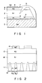
- An application of the technique will be described below with reference to Fig. 1.
- a silicon laminated structure consisting of a p-type P1 layer 1, an n-type N1 layer 2, a p-type P2 layer 3, and an n-type N2 layer 4 is formed first.
- the P1 layer is then brazed to an anode electrode plate 5 consisting of Mo or W by using an Al layer 6 as a solder.
- gate and cathode electrodes 7 and 8 are respectively formed on the P2 and N2 layers.
- the P1 layer may be fused in the Al layer 6 as a solder, so that the solder 6 and the N1 layer 2 may be brought into contact with each other at, e.g., a portion denoted by reference symbol A.
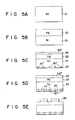
- a conventional technique for preventing this will be described below with reference to Figs. 2 and 3.
- Fig. 2 shows an anode short type GTO whose anode side is patterned.
- an N1+ layer is partially diffused first, and a P1 layer is formed by diffusion.
- the N1+ and P1 layers are formed deep.
- a portion X N1+ is expanded, and a portion X P1 is reduced accordingly.
- an effective region of a current flow is reduced.
- fine control during patterning becomes difficult. Therefore, variations in GTO characteristics occur.
- a GTO having an arrangement shown in Fig. 3 will be described below.
- a P1 layer is diffused deep first, and an N1+ layer is diffused.
- This method is advantageous in that a portion X N1+ can be formed to be narrow.
- the P1 layer cannot be controlled due to lateral diffusion.
- a resistance component R shown in Fig. 3 near the N1+ layer is increased, and the electrical characteristics are degraded.
- the first object can be achieved by a semiconductor device comprising: a substrate of a first conductivity type; a first layer of a second conductivity type formed on one surface of said first substrate of the first conductivity type; a second layer of the first conductivity type formed on the first layer of the second conductivity type; a third layer of the first conductivity type selectively formed on the other surface of the substrate of the first conductivity type; and a fourth layer of the second conductivity type formed on the other surface of the substrate of the first conductivity type, a vertical dimension of the fourth layer being larger than that of the first layer.
- the second object can be achieved by a method of manufacturing a semiconductor device, comprising the steps of: providing a substrate of a first conductivity type which has a relatively high resistivity; forming a first layer of a second conductivity type on one surface of the substrate; forming a second layer of the first conductivity type on one surface of the first layer; selectively forming a third layer of the first conductivity type on the other surface of the substrate; forming a fourth layer of the second conductivity type on the other surface of the substrate so as to be shallower than the first and third layers and to have an impurity concentration higher than that of the substrate and lower than that of the third layer; forming a gate electrode on a selected portion of the one surface of the first layer; forming a first main electrode on one surface of the second layer; and forming a second main electrode on the third and fourth layers.
- Fig. 4 is a sectional view showing an arrangement of a GTO body of a semiconductor device of the present invention.
- Reference numeral 21 denotes an n-type silicon substrate (N1) layer; 22, a p-type base layer (P2) layer formed on a surface of the N1 layer by diffusion; 23, an n+-type emitter layer (N2+ layer) formed on the upper surface of the P2 layer by diffusion; 24, an n+-type base layer (N1+ layer) selectively formed on the lower surface of the N1 layer by diffusion; and 25, a p-type emitter layer (P1 layer) formed on the lower surface of the N1 layer by diffusion.
- Anode, cathode, and gate electrode films (not shown in Fig.
- the respective electrode films are formed by deposition methods such as evaporation and sputtering.
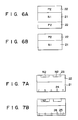
- Figs. 5A to 5E are views showing a method of manufacturing the GTO body in Fig. 4.
- the n-type silicon substrate 21 is prepared.
- the P2 layer 22 is formed on a surface of the substrate 21 by diffusion (Fig. 5B). At this time, Ga or B is used as a dopant.
- the P2 layer 22 has a surface concentration of about 1 ⁇ 1018 cm ⁇ 3 and a diffusion depth of about 60 ⁇ m.
- the P2 layers may be formed on the upper and lower surfaces of the substrate as shown in Fig. 6A instead of employing the arrangement in Fig. 5A, and the P2 layer on one surface may then be removed as shown in Fig. 6B.
- the N1+ layer 24 is selectively formed on the anode side surface
- the N2+ layer 23 is formed on the entire cathode side surface by diffusion.
- the P1 layer 25 is formed on the resultant structure by diffusion so as to have a lower impurity concentration than the N1+ layer and a higher impurity concentration than the substrate 21 (Fig. 5D). With this process, the P1 and N1+ layers are selectively formed on the anode side.
- Fig. 5E surfaces of the N2+ and P2 layers are partially removed, and the surface of the P2 layer is partially exposed. Note that if the N2 layer is selectively formed by diffusion as shown in Fig. 7A, an arrangement shown in Fig. 7B can be obtained without the step of removing the surfaces of the N2 and P2 layers as shown in Fig. 5E.
- the P1 layer preferably has a thickness of 5 to 20 ⁇ m. If the thickness is 5 ⁇ m or less, the current injection efficiency from the P1 layer to the N1 layer is decreased, and a current amplification factor ⁇ PNP is decreased, resulting in degradation in ON characteristics. If the thickness is 20 ⁇ m or more, lateral diffusion occurs, and fine control is difficult to perform, as described above.
- an SiO2 film 31 is formed across the P2 and N2 layers so as to passivate the P2-N2 junction.
- Anode, cathode, and gate electrodes 32, 33, and 34 are respectively formed on the P1 and N1+ layers, the N2 layer, and the P2 layer by, e.g., Al evaporation.
- a polyimide film 35 is then partially coated on the gate electrode 34.
- a peripheral portion of the resultant structure is beveled, and a silicone resin 36 is coated thereon.
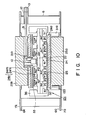
- a semiconductor pellet 121 has a four-layered structure consisting of a P1 emitter layer 25, an N1+ base layer 24, a P2 base layer 22, and an N2+ emitter layer 23 which are arranged in this order from a second major surface (lower surface in Fig. 10) to a first major surface (upper surface in Fig. 10).
- the P1 emitter layer 25 is locally formed, and part of the N1+ base layer 24 is exposed from the second major surface (anode side).
- the emitter layer 23 is divided into a large number of layers.
- a main electrode (cathode electrode) 33 is formed on the N2+ emitter layer 23 on the first major surface of the semiconductor pellet 121; and a control electrode (gate electrode) 34, on the base layer 22.
- the main electrode 33 is surrounded by the control electrode 34, i.e., both the electrodes are formed on one major surface in a complex manner.
- a main electrode (anode electrode) 32 is formed on the other major surface (second major surface) to short-circuit the P1 emitter layer 25 and the partially exposed N1+ base layer 24, thus forming a so-called anode short structure.
- the cathode electrode 33 on the first major surface of the semiconductor pellet 121 is urged by a cathode electrode post 23k through a cathode side electrode member 24k consisting of an electrode plate 24m and a thin soft metal plate 24n.
- the anode electrode 32 on the second major surface is urged by an anode electrode post 23a through an anode side electrode member 24a.
- a gate lead 9 is arranged in hollow and notched portions of the electrode post 23k and the electrode member 24k through a positioning guide 31k made of an insulating material and an insulating member (not shown).
- One end of the gate lead 9 is urged against the gate electrode 34 by a gate urge spring 10, and the other end thereof is inserted in a metal sleeve 12 brazed to a side wall of a cylindrical insulating member 6 and extends outside the sleeve 12 to be sealed by a seal portion 13.
- cathode electrode post 23k, anode electrode post 23a, and cylindrical insulating member 6 are silver-brazed and arc-welded to each other through circular metal plates (weld rings) 6k, 6a, 7k, and 7a and therefore constitute an enclosure for airtight sealing the semiconductor pellet 121.
- the insulating member 6 is made of ceramic material while the metal plates 6k, 6a, 7k, and 7a cobalt.
- the anode side electrode member 24a and anode electrode post 23a are positioned by a positioning guide 31a.
- the positioning guide 31a is an annular cylindrical member made of metal such as aluminum or such insulators as Teflon and epoxy resin and has a stepped portion on the inner circumferential face to prevent the vibrational movement thereof.
- the manufacturing method described above is not much different from the conventional method, and allows relatively easy manufacture of the semiconductor device of the present invention at a low cost.
- a substrate N1 of a first conductivity type which has a relatively high resistivity is prepared.
- a first layer P2 of a second conductivity type is formed on a surface of the substrate N1 (Fig. 11B).
- a second layer P1 of the second conductivity type is formed on the lower surface of the substrate N1 so as to be thinner than the first layer P2 (Fig. 11C).
- a third layer N2 of the first conductivity type is formed on the first layer P2, whereas a fourth layer N1+ of the first conductivity type which has a higher impurity concentration than the second layer P1 is selectively formed thereon.
- the N2 and P2 layers are partially removed to expose part of the surface of the P2 layer.
- a gate electrode, a first main electrode, and a second main electrode are respectively formed on the exposed surface of the first layer P2, the surface of the third layer N2, and the second and fourth layers P1 and N1+ by a deposition method.
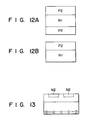
- P2 layers may be formed on the upper and lower surfaces of the substrate, as shown in Fig. 12A, instead of employing the arrangement shown in Fig. 11B, and the P2 layer on one surface may be removed, as shown in Fig. 12B.
- the step of removing the layers N2 and P2 in Fig. 11E can be omitted.
- the second embodiment has the following advantages. Since the depth of the second layer can be arbitrarily controlled in the second step (Fig. 11C), balanced characteristics can be obtained. In addition, since the fourth layer has a higher impurity concentration and a higher impurity diffusion coefficient than the second layer, the fourth layer can be formed to be deeper than the second layer.
Landscapes
- Thyristors (AREA)
- Electrodes Of Semiconductors (AREA)
Applications Claiming Priority (2)
| Application Number | Priority Date | Filing Date | Title |
|---|---|---|---|
| JP250456/88 | 1988-10-04 | ||
| JP25045688 | 1988-10-04 |
Publications (3)
| Publication Number | Publication Date |
|---|---|
| EP0366916A2 true EP0366916A2 (de) | 1990-05-09 |
| EP0366916A3 EP0366916A3 (de) | 1991-08-28 |
| EP0366916B1 EP0366916B1 (de) | 1995-06-14 |
Family
ID=17208146
Family Applications (1)
| Application Number | Title | Priority Date | Filing Date |
|---|---|---|---|
| EP89117033A Expired - Lifetime EP0366916B1 (de) | 1988-10-04 | 1989-09-14 | Halbleiteranordnung mit kurzgeschlossener Anode und Verfahren zu deren Herstellung |
Country Status (3)
| Country | Link |
|---|---|
| US (1) | US5148254A (de) |
| EP (1) | EP0366916B1 (de) |
| DE (1) | DE68923056T2 (de) |
Cited By (5)
| Publication number | Priority date | Publication date | Assignee | Title |
|---|---|---|---|---|
| US5204273A (en) * | 1990-08-20 | 1993-04-20 | Siemens Aktiengesellschaft | Method for the manufacturing of a thyristor with defined lateral resistor |
| EP0631321A1 (de) * | 1993-06-22 | 1994-12-28 | Hitachi, Ltd. | Gate-Turn-off-Thyristor |
| DE4337209A1 (de) * | 1993-10-30 | 1995-05-04 | Abb Management Ag | Abschaltbarer Thyristor |
| DE4431294A1 (de) * | 1994-09-02 | 1996-03-07 | Abb Management Ag | Abschaltbarer Thyristor für hohe Blockierspannungen und kleiner Bauelementdicke |
| EP0676813A3 (de) * | 1994-04-04 | 1999-06-02 | Mitsubishi Denki Kabushiki Kaisha | Gate-Turn-off-Thyristor und Verfahren zu seiner Herstellung |
Families Citing this family (1)
| Publication number | Priority date | Publication date | Assignee | Title |
|---|---|---|---|---|
| US5962878A (en) * | 1997-09-17 | 1999-10-05 | Citizen Watch Co., Ltd. | Surge protection device and method of fabricating the same |
Family Cites Families (21)
| Publication number | Priority date | Publication date | Assignee | Title |
|---|---|---|---|---|
| US3251004A (en) * | 1961-04-27 | 1966-05-10 | Merck & Co Inc | Relaxation oscillator semiconductor solid circuit structure |
| US4009059A (en) * | 1972-01-08 | 1977-02-22 | Mitsubishi Denki Kabushiki Kaisha | Reverse conducting thyristor and process for producing the same |
| CH543178A (de) * | 1972-03-27 | 1973-10-15 | Bbc Brown Boveri & Cie | Kontinuierlich steuerbares Leistungshalbleiterbauelement |
| DE2636234A1 (de) * | 1976-08-12 | 1978-02-16 | Bbc Brown Boveri & Cie | Steuerbares halbleiterbauelement fuer zwei stromrichtungen |
| JPS54111790A (en) * | 1978-02-22 | 1979-09-01 | Hitachi Ltd | Semiconductor switchgear |
| JPS6043032B2 (ja) * | 1978-09-14 | 1985-09-26 | 株式会社日立製作所 | ゲートターンオフサイリスタ |
| JPS6019147B2 (ja) * | 1979-01-24 | 1985-05-14 | 株式会社日立製作所 | ゲ−ト・タ−ン・オフ・サイリスタ |
| JPS571257A (en) * | 1980-06-04 | 1982-01-06 | Hitachi Ltd | Semiconductor device |
| JPS5773956A (en) * | 1980-10-27 | 1982-05-08 | Hitachi Ltd | Glass coated semiconductor device |
| JPS57201077A (en) * | 1981-06-05 | 1982-12-09 | Hitachi Ltd | Semiconductor switching device |
| JPS59134876A (ja) * | 1983-01-20 | 1984-08-02 | Mitsubishi Electric Corp | 半導体装置 |
| JPS6085563A (ja) * | 1983-10-17 | 1985-05-15 | Mitsubishi Electric Corp | ゲ−ト・タ−ンオフサイリスタの製造方法 |
| JPS60119776A (ja) * | 1983-11-30 | 1985-06-27 | Mitsubishi Electric Corp | ゲ−トタ−ンオフサイリスタ |
| GB2150753B (en) * | 1983-11-30 | 1987-04-01 | Toshiba Kk | Semiconductor device |
| EP0178387B1 (de) * | 1984-10-19 | 1992-10-07 | BBC Brown Boveri AG | Abschaltbares Leistungshalbleiterbauelement |
| US4757025A (en) * | 1985-03-25 | 1988-07-12 | Motorola Inc. | Method of making gate turn off switch with anode short and buried base |
| JPH0715991B2 (ja) * | 1985-06-12 | 1995-02-22 | 株式会社東芝 | 半導体装置の製造方法 |
| DE3628857A1 (de) * | 1985-08-27 | 1987-03-12 | Mitsubishi Electric Corp | Halbleitereinrichtung |
| JPS63209167A (ja) * | 1987-02-26 | 1988-08-30 | Hitachi Ltd | 半導体装置の製造方法 |
| US4951110A (en) * | 1987-11-03 | 1990-08-21 | Siemens Aktiengesellschaft | Power semiconductor structural element with four layers |
| DE3742638A1 (de) * | 1987-12-16 | 1989-06-29 | Semikron Elektronik Gmbh | Gto-thyristor |
-
1989
- 1989-09-14 EP EP89117033A patent/EP0366916B1/de not_active Expired - Lifetime
- 1989-09-14 DE DE68923056T patent/DE68923056T2/de not_active Expired - Fee Related
-
1990
- 1990-12-28 US US07/633,186 patent/US5148254A/en not_active Expired - Lifetime
Cited By (8)
| Publication number | Priority date | Publication date | Assignee | Title |
|---|---|---|---|---|
| US5204273A (en) * | 1990-08-20 | 1993-04-20 | Siemens Aktiengesellschaft | Method for the manufacturing of a thyristor with defined lateral resistor |
| EP0631321A1 (de) * | 1993-06-22 | 1994-12-28 | Hitachi, Ltd. | Gate-Turn-off-Thyristor |
| US5554863A (en) * | 1993-06-22 | 1996-09-10 | Hitachi, Ltd. | Gate turn-off thyristor |
| DE4337209A1 (de) * | 1993-10-30 | 1995-05-04 | Abb Management Ag | Abschaltbarer Thyristor |
| US5491351A (en) * | 1993-10-30 | 1996-02-13 | Abb Management Ag | Gate turn-off thyristor |
| EP0676813A3 (de) * | 1994-04-04 | 1999-06-02 | Mitsubishi Denki Kabushiki Kaisha | Gate-Turn-off-Thyristor und Verfahren zu seiner Herstellung |
| DE4431294A1 (de) * | 1994-09-02 | 1996-03-07 | Abb Management Ag | Abschaltbarer Thyristor für hohe Blockierspannungen und kleiner Bauelementdicke |
| US5710445A (en) * | 1994-09-02 | 1998-01-20 | Asea Brown Boveri Ag | Gate turn-off thyristor for high blocking voltage and small component thickness |
Also Published As
| Publication number | Publication date |
|---|---|
| EP0366916A3 (de) | 1991-08-28 |
| US5148254A (en) | 1992-09-15 |
| EP0366916B1 (de) | 1995-06-14 |
| DE68923056D1 (de) | 1995-07-20 |
| DE68923056T2 (de) | 1995-11-30 |
Similar Documents
| Publication | Publication Date | Title |
|---|---|---|
| CN102163626B (zh) | 具有新的保护环终端设计的功率半导体器件及其生产方法 | |
| EP0345435B2 (de) | Halbleiteranordnung mit hoher Durchbruchspannung und Verfahren für ihre Herstellung | |
| US4996586A (en) | Crimp-type semiconductor device having non-alloy structure | |
| EP0009367A1 (de) | Durch eine Steuerelektrode abschaltbarer Thyristor | |
| EP0428044A2 (de) | Hochleistungshalbleiteranordnung mit Gehäuse | |
| US3923975A (en) | Tantalum-gallium arsenide schottky barrier semiconductor device | |
| US5248622A (en) | Finely controlled semiconductor device and method of manufacturing the same | |
| EP0366916B1 (de) | Halbleiteranordnung mit kurzgeschlossener Anode und Verfahren zu deren Herstellung | |
| US3975758A (en) | Gate assist turn-off, amplifying gate thyristor and a package assembly therefor | |
| EP0421344B1 (de) | Leistungshalbleiteranordnung vom Drucktyp | |
| US5223442A (en) | Method of making a semiconductor device of a high withstand voltage | |
| US3671821A (en) | Semiconductor controlled rectifier including two emitter regions | |
| JP3718223B2 (ja) | 縦の溝を有する高電圧用の半導体デバイス | |
| US5344794A (en) | Method of making a semiconductor chip | |
| EP0235706A2 (de) | Thyristor mit einem mit seinem Gate gekoppelten Widerstandselement und Verfahren zu dessen Herstellung | |
| JP3226528B2 (ja) | 半導体装置及びその製造方法 | |
| JPH07249737A (ja) | プレーナ型半導体装置およびその製造方法 | |
| EP0472262B1 (de) | Heteroübergang-Bipolartransistor | |
| US3270255A (en) | Silicon rectifying junction structures for electric power and process of production thereof | |
| JP3255698B2 (ja) | 高安定ツェナーダイオード | |
| JP2002064200A (ja) | 半導体装置 | |
| JPS59159567A (ja) | 光駆動型半導体制御整流装置 | |
| JPH0832049A (ja) | 半導体装置 | |
| CN121152224A (zh) | 一种frd器件及其制备方法 | |
| JPH06244408A (ja) | 双方向型半導体装置の製造方法 |
Legal Events
| Date | Code | Title | Description |
|---|---|---|---|
| PUAI | Public reference made under article 153(3) epc to a published international application that has entered the european phase |
Free format text: ORIGINAL CODE: 0009012 |
|
| 17P | Request for examination filed |
Effective date: 19890914 |
|
| AK | Designated contracting states |
Kind code of ref document: A2 Designated state(s): CH DE FR GB LI SE |
|
| PUAL | Search report despatched |
Free format text: ORIGINAL CODE: 0009013 |
|
| AK | Designated contracting states |
Kind code of ref document: A3 Designated state(s): CH DE FR GB LI SE |
|
| 16A | New documents despatched to applicant after publication of the search report | ||
| 17Q | First examination report despatched |
Effective date: 19930922 |
|
| GRAA | (expected) grant |
Free format text: ORIGINAL CODE: 0009210 |
|
| AK | Designated contracting states |
Kind code of ref document: B1 Designated state(s): CH DE FR GB LI SE |
|
| REF | Corresponds to: |
Ref document number: 68923056 Country of ref document: DE Date of ref document: 19950720 |
|
| ET | Fr: translation filed | ||
| RIN2 | Information on inventor provided after grant (corrected) |
Free format text: MATSUDA, HIDEO C/O INTELLECTUAL PROPERTY DIVISION * YOSHIDA, TAKEOMI C/O INTELLECTUAL PROPERTY * FUJIWARA, TAKASHI C/O INTELLECTUAL PROPERTY DIVSN |
|
| PLBE | No opposition filed within time limit |
Free format text: ORIGINAL CODE: 0009261 |
|
| STAA | Information on the status of an ep patent application or granted ep patent |
Free format text: STATUS: NO OPPOSITION FILED WITHIN TIME LIMIT |
|
| 26N | No opposition filed | ||
| REG | Reference to a national code |
Ref country code: GB Ref legal event code: 746 Effective date: 19981103 |
|
| REG | Reference to a national code |
Ref country code: FR Ref legal event code: D6 |
|
| REG | Reference to a national code |
Ref country code: GB Ref legal event code: IF02 |
|
| PGFP | Annual fee paid to national office [announced via postgrant information from national office to epo] |
Ref country code: DE Payment date: 20070906 Year of fee payment: 19 |
|
| REG | Reference to a national code |
Ref country code: CH Ref legal event code: PFA Owner name: KABUSHIKI KAISHA TOSHIBA Free format text: KABUSHIKI KAISHA TOSHIBA#72 HORIKAWA-CHO SAIWAI-KU#KAWASAKI-SHI/KANAGAWA-KEN (JP) -TRANSFER TO- KABUSHIKI KAISHA TOSHIBA#72 HORIKAWA-CHO SAIWAI-KU#KAWASAKI-SHI/KANAGAWA-KEN (JP) |
|
| PGFP | Annual fee paid to national office [announced via postgrant information from national office to epo] |
Ref country code: CH Payment date: 20070913 Year of fee payment: 19 |
|
| PGFP | Annual fee paid to national office [announced via postgrant information from national office to epo] |
Ref country code: GB Payment date: 20070912 Year of fee payment: 19 |
|
| PGFP | Annual fee paid to national office [announced via postgrant information from national office to epo] |
Ref country code: SE Payment date: 20070905 Year of fee payment: 19 |
|
| PGFP | Annual fee paid to national office [announced via postgrant information from national office to epo] |
Ref country code: FR Payment date: 20070914 Year of fee payment: 19 |
|
| REG | Reference to a national code |
Ref country code: CH Ref legal event code: PL |
|
| GBPC | Gb: european patent ceased through non-payment of renewal fee |
Effective date: 20080914 |
|
| REG | Reference to a national code |
Ref country code: FR Ref legal event code: ST Effective date: 20090529 |
|
| PG25 | Lapsed in a contracting state [announced via postgrant information from national office to epo] |
Ref country code: DE Free format text: LAPSE BECAUSE OF NON-PAYMENT OF DUE FEES Effective date: 20090401 |
|
| PG25 | Lapsed in a contracting state [announced via postgrant information from national office to epo] |
Ref country code: LI Free format text: LAPSE BECAUSE OF NON-PAYMENT OF DUE FEES Effective date: 20080930 Ref country code: FR Free format text: LAPSE BECAUSE OF NON-PAYMENT OF DUE FEES Effective date: 20080930 Ref country code: CH Free format text: LAPSE BECAUSE OF NON-PAYMENT OF DUE FEES Effective date: 20080930 |
|
| PG25 | Lapsed in a contracting state [announced via postgrant information from national office to epo] |
Ref country code: GB Free format text: LAPSE BECAUSE OF NON-PAYMENT OF DUE FEES Effective date: 20080914 |
|
| PG25 | Lapsed in a contracting state [announced via postgrant information from national office to epo] |
Ref country code: SE Free format text: LAPSE BECAUSE OF NON-PAYMENT OF DUE FEES Effective date: 20080915 |