EP0366949B1 - Dispositif Josephson et procédé de sa fabrication - Google Patents
Dispositif Josephson et procédé de sa fabrication Download PDFInfo
- Publication number
- EP0366949B1 EP0366949B1 EP89118259A EP89118259A EP0366949B1 EP 0366949 B1 EP0366949 B1 EP 0366949B1 EP 89118259 A EP89118259 A EP 89118259A EP 89118259 A EP89118259 A EP 89118259A EP 0366949 B1 EP0366949 B1 EP 0366949B1
- Authority
- EP
- European Patent Office
- Prior art keywords
- layer
- thin film
- superconductor thin
- oxide superconductor
- shaped
- Prior art date
- Legal status (The legal status is an assumption and is not a legal conclusion. Google has not performed a legal analysis and makes no representation as to the accuracy of the status listed.)
- Expired - Lifetime
Links
Images


Classifications
-
- H—ELECTRICITY
- H10—SEMICONDUCTOR DEVICES; ELECTRIC SOLID-STATE DEVICES NOT OTHERWISE PROVIDED FOR
- H10N—ELECTRIC SOLID-STATE DEVICES NOT OTHERWISE PROVIDED FOR
- H10N60/00—Superconducting devices
- H10N60/01—Manufacture or treatment
- H10N60/0912—Manufacture or treatment of Josephson-effect devices
- H10N60/0941—Manufacture or treatment of Josephson-effect devices comprising high-Tc ceramic materials
-
- Y—GENERAL TAGGING OF NEW TECHNOLOGICAL DEVELOPMENTS; GENERAL TAGGING OF CROSS-SECTIONAL TECHNOLOGIES SPANNING OVER SEVERAL SECTIONS OF THE IPC; TECHNICAL SUBJECTS COVERED BY FORMER USPC CROSS-REFERENCE ART COLLECTIONS [XRACs] AND DIGESTS
- Y10—TECHNICAL SUBJECTS COVERED BY FORMER USPC
- Y10S—TECHNICAL SUBJECTS COVERED BY FORMER USPC CROSS-REFERENCE ART COLLECTIONS [XRACs] AND DIGESTS
- Y10S505/00—Superconductor technology: apparatus, material, process
- Y10S505/70—High TC, above 30 k, superconducting device, article, or structured stock
- Y10S505/701—Coated or thin film device, i.e. active or passive
- Y10S505/702—Josephson junction present
-
- Y—GENERAL TAGGING OF NEW TECHNOLOGICAL DEVELOPMENTS; GENERAL TAGGING OF CROSS-SECTIONAL TECHNOLOGIES SPANNING OVER SEVERAL SECTIONS OF THE IPC; TECHNICAL SUBJECTS COVERED BY FORMER USPC CROSS-REFERENCE ART COLLECTIONS [XRACs] AND DIGESTS
- Y10—TECHNICAL SUBJECTS COVERED BY FORMER USPC
- Y10S—TECHNICAL SUBJECTS COVERED BY FORMER USPC CROSS-REFERENCE ART COLLECTIONS [XRACs] AND DIGESTS
- Y10S505/00—Superconductor technology: apparatus, material, process
- Y10S505/825—Apparatus per se, device per se, or process of making or operating same
- Y10S505/873—Active solid-state device
- Y10S505/874—Active solid-state device with josephson junction, e.g. squid
Definitions
- the present invention relates to tunnel junction type Josephson devices using an oxide superconductor and a process for manufacturing the same.
- NbN niobium nitride
- Nb 3 Ge germanium niobium
- Ba-La-Cu-O type high temperature superconductor is proposed [J. G. Bednorz and K. A. Müller, Zeitschrift for Physik B - Condensed Matter, 64 , 189-193 (1986)].
- oxide superconductors discovered recently have a superconducting transition temperature exceeding the temperature of liquid nitrogen (77.3 K), and thus this discovery is considered to enlarge the fields to which superconductors are applied.
- a Bi-Sr-Ca-Cu-O type superconductor composed of a Bi type layer-shaped oxide exhibits a superconducting transition temperature equal to or higher than 100 K. [H. Maeda, Y. Tanaka, M. Fukutomi and T. Asano, Japanese Journal of Applied Physics, 27 , L209-L210 (1988)].
- Tl-Ba-Ca-Cu-O type material exhibits a superconducting transition at 120 K or more and it is found that this is a layer-shaped oxide like a Bi type layer-shaped oxide [Z. Z. Sheng and A. M. Hermann, Nature, 332 , 138-139 (1988)].
- the superconducting mechanism of this kind of materials is not known in detail, there is a possibility that a transition temperature thereof exceeds a room temperature. Then, they are expected to have more hopeful characteristics as a superconductor than conventional binary compounds.
- a Josephson device having a Josephson junction using a superconductor is known as a typical superconductive device.
- Josephson junctions include a tunnel junction type composed of superconductors disposed on opposite sides of a very thin insulating layer having a thickness of several nanometers (tens of angstrom), a bridge type composed of a single superconductor having a thin part contracted to the size of 1 ⁇ m, a point contact type using a sharp stylus composed of a superconductor and the like.
- the Josephson devices of the above types except the tunnel junction type require a super-fine pattern lithography technology with a result of low reproducibility and yield, and thus it is very difficult to integrate many Josephson devices. Therefore, they are mainly manufactured using the conventional superconductor such as a binary compound.
- a broken type Josephson device composed of an oxide superconductor which is divided into two parts and has a slight contact made therebetween; a bridge type Josephson device composed of a thin film of an oxide superconductor having a small construction; and a proximity effect bridge type Josephson device composed of oxide superconductors coupled a noble metal such as Au, Ag or the like.
- a tunnel type Josephson device is manufactured as a prototype which is composed of an oxide superconductor such as Y-Ba-Cu-O, Bi-Sr-Ca-Cu-O, Tl-Ba-Ca-Cu-O or the like and a metal superconductor such as Nb, Pb or the like.
- oxide superconductor such as Y-Ba-Cu-O, Bi-Sr-Ca-Cu-O, Tl-Ba-Ca-Cu-O or the like
- a metal superconductor such as Nb, Pb or the like.
- EP-0 342 038 A2 falling within the terms of Article 54(3) EPC, published on November 15, 1989, i.e. after the filing of the present patent application, discloses a Josephson device and a method for producing the same.
- the Josephson device according to said document comprises first and second layer-shaped oxide superconductor thin films each comprising a bismuth-copper-containing oxide superconductor and a barrier layer therebetween.
- the barrier layer comprises an oxide containing Bi.
- US-PS 4,499,119 shows a Josephson device comprising a barrier layer made of Si, Ge or alloys thereof.
- JP-A-58-002 082 and JP-A-58-077 265 describe a Josephson device having a barrier layer made of silicon nitride.
- JP-A-61-220 385 discloses a Josephson device with a barrier layer made of magnesium oxide.
- the object underlying the invention is to provide a Josephson device and a process for producing the same, which Josephson device has an excellent tunnel junction.
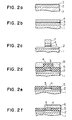
- the first layer-shaped oxide superconductor thin film 2 is formed on a substrate 1
- a barrier layer 3 is formed on the thin film 2
- the second layer-shaped oxide superconductor thin film 4 is formed to provide a junction.
- An interlayer insulating film 5 is formed in such a manner that it surrounds the junction.
- a layer-shaped oxide superconductor thin film 6 for a contact is formed on the interlayer insulating film 5 so that the thin film 6 is brought into contact with the second layer-shaped oxide superconductor thin film 4.
- a Josephson device according to the present invention is manufactured.
- the Bi type layer-shaped oxide superconductor thin film 2 mainly composed of Bi 2 Sr 2 Ca 1 Cu 2 O y is formed to a thickness of 300 nm at a substrate temperature of about 700°C by an rf magnetron sputtering method, and the barrier layer 3 is formed to a thickness of 2 nm in the same vacuum [Figure 2a].
- a material familiar with the layer-shaped oxide superconductor thin film 2 is used as the barrier layer 3, and a Bi oxide is used.
- a material of the barrier layer 3 must be carefully selected since problems arise in that when the substrate 1 is heated to further form the layer-shaped oxide superconductor thin films 4 and 6, the barrier layer 3 is diffused and deteriorates the layer-shaped oxide superconductor thin film 2 or 4 and the like, or the barrier layer 3 is broken to cause the layer-shaped oxide superconductor thin films 2 and 4 to be short-circuited.
- the barrier layer As a material of the barrier layer, there is used bismuth oxide alone or in admixture with strontium oxide, calcium oxide, barium oxide, zinc oxide, magnesium oxide, and zirconium oxide and the like. These materials do not cause a mutual diffusion, and even if the mutual diffusion is caused, they are less deteriorated since they are composed of a material similar to the Bi oxide type layer-shaped oxide superconductor thin film.
- a Bi oxide type layer-shaped compound is used as a material of the barrier layer 3. It is found that when a Bi oxide type layer-shaped compound containing at least one selected from the group consisting of Ti, Nb, Ta and W is used as a material of the barrier layer 3, a tunnel junction with a less current leakage can be also provided likewise.
- an excellent tunnel junction can be formed likewise when a material of the barrier layer 3 is composed of a Bi oxide type layer-shaped compound containing at least one selected from the group consisting of Ti, Nb and Ta and at least one selected from the group consisting of Pb, Ca, Sr and Ba; a Bi oxide type layer-shaped compound containing Ti and at least one metal selected from the group consisting of Na, K, Fe, Nb and Ta; or a Bi oxide type layer-shaped compound containing Nb and K. Furthermore, when Bi 2 Ti 4 O 11 or Bi 4 Ti 3 O 12 is used as a material of the barrier layer 3, an excellent tunnel junction can be formed.
- the second layer-shaped oxide superconductor thin film 4 is further formed to a thickness of about 400 nm in the same vacuum by an rf magnetron spattering method [Figure 2b].
- a temperature of the substrate is about 700°C.
- a resist pattern 7 is formed to a thickness of about 1 ⁇ m on the thin films continuously formed as described above by a photolithographic process, and etching is effected thereto by an Ar ion milling to expose the first layer-shaped oxide superconductor thin film 2 [ Figure 2c].
- the resist 7 is removed by irradiation of O 2 plasma or the like and then the interlayer insulating film 5 is formed.
- a material similar to one used for the barrier layer 3 can be used.
- a spin-on-glass 8 is applied on the interlayer insulating layer by a spinner and baked to be flown so that the surface thereof is made flat [Figure 2d]. Then, the surface thereof is etched with Ar ion [ Figure 2e]. The surface of the second layer-shaped oxide superconductor thin film 4 is exposed in this step. Further, the layer-shaped oxide superconductor thin film 6 for a contact is formed on the second layer-shaped oxide superconductor thin film 4 and the layer-shaped oxide superconductor thin film for a contact 6 is patterned by photolithography and etching, whereby a Josephson device is manufactured.
- Figure 3 shows process diagrams of an embodiment of a process for manufacturing a Josephson device according to the present invention.
- the first layer-shaped oxide superconductor thin film 2 (film thickness: 300 nm) of Bi-Sr-Ca-Cu-O type is formed on a substrate 1 making use of a (100) surface of MgO at a substrate temperature of about 700°C by an rf magnetron spattering method and then Bi 4 Ti 3 O 12 is deposited as a barrier layer 3 (film thickness: 2 nm) by an rf magnetron spattering method while the vacuum is maintained [Figure 3a]. Then, the first layer-shaped oxide superconductor thin film 2 is patterned by photolithography and Ar ion milling [Figure 3b].
- a negative type resist is spin-coated to a thickness of 8.0 nm as a protective layer and a positive type resist is spin-coated thereon to a thickness of 800 nm, and then they are exposed and developed to define a pattern of a resist 7 which is formed only in a region serving as a junction and a contact portion of the first layer-shaped oxide superconductor thin film 2.
- Bi 4 Ti 3 O 12 is deposited thereon to a thickness of 300 nm by an rf magnetron spattering method to form an interlayer insulating film 5 [Figure 3c]. The specimen was immersed in acetone and slightly subjected to ultrasonic waves for lifting off [Figure 3d].
- the second oxide superconductor thin film 4 is formed in the same vacuum at a substrate temperature of 700°C by an rf magnetron sputtering method. A film thickness thereof is 300 nm.
- a resist pattern 9 is formed thereon to pattern the second oxide superconductor thin film 4 by ordinary photolithography [ Figure 3e]. Etching is effected by an Ar ion milling so that the second oxide superconductor thin film 4 is patterned and simultaneously a window is defined to the barrier layer 3 for a contact with the first oxide superconductor thin film 2.
- the remaining resist pattern 9 is removed by ashing in oxygen plasma and then a Josephson device is formed by being heated at 845°C in an oxygen atmosphere for four hours and annealed by being cooled in a furnace to a room temperature [Figure 3f].
- the Josephson device manufactured as described above corresponds to a structure wherein the second layer-shaped oxide superconductor thin film 4 and the layer-shaped oxide superconductor thin film for a contact 6 are composed of the same material and united in Figure 1.
- Figure 4 shows a cross sectional view of an embodiment of Josephson device according to the present invention.
- Figure 5 shows an embodiment of process for manufacturing it.
- the first layer-shaped oxide superconductor thin film 2 is formed on a substrate 1, a thin metal film 10 is formed thereon and a barrier layer 3 and then the second layer-shaped oxide superconductor thin film 4 are further formed thereon to form a Josephson junction 11 which is surrounded by an interlayer insulating film 5.
- the lower portion of the interlayer insulating film 5 is in contact with the surface of the thin metal film 10, and a part of the upper surface thereof is in contact with a layer-shaped oxide superconductor thin film 6 for wiring.
- the layer-shaped oxide superconductor thin film 6 for wiring is in contact with the second layer-shaped oxide superconductor thin film 4 at a part of the lower surface thereof to form a superconductive contact and serves as an upper electrode of a Josephson junction.
- a layer-shaped oxide superconductor thin film 4' for a contact directly formed on the thin metal film 10 forms a super-conductive contact with the first layer-shaped oxide superconductor thin film 2 through the thin metal film 10 due to a proximity effect and serves as a lead electrode of a lower electrode of the junction.
- the first layer-shaped oxide superconductor thin film 2 (film thickness: 300 nm) of Bi-Sr-Ca-Cu-O type is formed on a substrate 1 using a MgO (100) surface at a substrate temperature of 700°C by an rf magnetron sputtering method.
- a composition of Bi : Sr Cu 1.6 : 1 : 1.5 : 2 and a sputtering is : Ca : effected in a mixed atmosphere of Ar and O 2 at 0.5 Pa.
- a thin metal film 10 composed of Au (film thickness: 10 nm) is formed thereon by a resistance heating method without breaking a vacuum and a barrier layer 3 composed of Bi 2 O 3 (film thickness: 2 nm) and acting as a tunnel barrier is formed thereon by an rf magnetron sputtering method.
- materials of the thin metal film 10 there are also used, alone or in admixture, Ag, Au, Pt, Pd and the like.
- a substrate temperature is preferably 400°C at this time.
- the second layer-shaped oxide superconductor thin film 4 composed of Bi-Sr-Ca-Cu-O is formed to a thickness of 300 nm without breaking the vacuum [ Figure 5a].
- the second layer-shaped oxide superconductor thin film 4 and the barrier layer 3 are patterned by a photolithographic process and Ar ion milling to form a junction 11 [Figure 5b].
- a resist 7 is preferably composed of a negative type spin-coated to a thickness of 80 nm and a positive type spin-coated thereon to a thickness of 800 nm as a protective layer. It is convenient that etching is effected until the surface of the thin metal film 10 is exposed.
- An accelerating voltage of Ar ion is preferably about 500 V.
- Bi 2 O 3 is deposited to a thickness of 300 nm at room temperature by an rf magnetron sputtering method to form an interlayer insulating film 5.
- layer-shaped oxide superconductor thin film 6 of Bi-Sr-Ca-Cu-O type for wiring is formed at a temperature of 700°C. A thickness thereof is 300 nm.
- a photoresist 9 is spin-coated thereon to a thickness 800 nm, exposed and developed, and thus a pattern is formed for wiring and for a superconductive contact of the first and second layer-shaped oxide superconductor thin films 2 and 4 [Figure 5d].
- the resist at this time can be either a negative type or a positive type.
- a layer-shaped oxide superconductor thin film 6 for wiring is etched by an Ar ion milling. Thereafter, the remaining resist 9 is removed by ashing in oxygen plasma. This is annealed in an oxygen atmosphere to form a Josephson device. The contamination of interfaces can be prevented by forming the first layer-shaped oxide superconductor thin film 2, the thin metal film 10, the barrier layer 3 and the second layer-shaped oxide superconductor thin film 4 sequentially without breaking the vacuum.
- the thin metal film 10 serves as a buffer layer against a mutual diffusion between the barrier layer 3 and the first layer-shaped oxide superconductor thin film 2 so that a degree of freedom for selecting a material of the barrier layer 3 is increased.
- a metal containing at least one selected from the group consisting of Ag, Au, Pt and Pd as the material of the thin metal film 10.
- a Y-Ba-Cu-O type, Bi-Pb-Sr-Ca-Cu-O type, Tl-Ba-Ca-Cu-O type, Tl-Pb-Sr-Ca-Cu-O type and the like are used as layer-shaped oxide superconductor of the above embodiments in addition to the Bi-Sr-Ca-Cu-O type.
- FIG. 6 schematically shows, as an example, a layer-shaped crystal structure of Bi 2 Sr 2 Ca 2 Cu 3 O y .
- Numeral 12 designates the first layer-shaped oxide superconductor thin film, and Figure 6 shows a substrate crystal unit portion of this thin film 12.
- this Cu-O layer is considered to make some contribution to superconductivity, this view does not yet come to conclusion at present.
- An embodiment of layer-shaped oxide superconductor thin film of Bi-Sr-Ca-Cu-O type will be described below in detail as an example.
- Respective simple substances or compounds constituting these superconductors are evaporated as evaporating sources and periodically deposited on a substrate in a gas containing oxygen at a substrate temperature of 400 - 900°C. It is found that when an evaporating rate from each evaporating source is regulated in this vapor deposition, a phase having a critical temperature of at least 100 K appears corresponding to a deposition cycle.
- the inventors have discovered that when a substrate temperature is, in particular, in a range of 500 - 900°C, a phase having excellent crystallinity and a critical temperature of at least 100 K can be formed.
- the thin film formed exhibits a superconducting transition of about 80 K in the state as it is.
- the superconducting thin film is manufactured at about 650°C or less to prevent diffusion occurring through a tunnel barrier layer at a Josephson junction.
- the first layer-shaped oxide superconductor thin film is formed as described above.
- the periodically laminated layers can be formed in such a manner that a shutter is opened and closed in front of the evaporating sources when an MBE apparatus or multi-source EB vapor deposition apparatus is used or a type of gas is changed when a vapor phase epitaxy is used.
- An excellent laminated films also can be formed by a sputtering method using a plasma discharge or laser beam. In this case, it is considered that a high oxygen gas pressure, sputtering discharge or the like in the sputtering is convenient for the formation of a phase composed of the Bi type layer-shaped composite oxide and having a critical temperature of at least 100 K.
- the Bi layer-shaped composite oxide preferably contains Pb.
- the formation of the first layer-shaped oxide superconductor thin film 2 on a substrate 1 by the method described above makes it easy to successively form a thin metal film 10 in the same vacuum chamber.
- the thin film superconductor can be formed by using, as one of a plurality of evaporating sources, a metal, alloy or metal compound.
- a specimen is taken out to the atmosphere to be subjected to necessary processings for a device making use of the Josephson junction using technologies such as photo-lithography, ion etching, chemical etching and the like, as shown in Figures 7b and 7c.
- this specimen is disposed again in the vacuum chamber and a barrier layer 3 is formed as an insulating layer for forming the Josephson junction on the surface of the specimen.
- the barrier layer 3 is conveniently formed by a sputtering method or EB vapor deposition method.
- a Josephson junction device exhibiting good superconducting characteristics can be reliably manufactured by forming the second layer-shaped oxide superconductor thin film 4 similar to the thin film 2 on the barrier layer 3 by the same method as above.
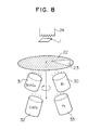
- sputtering is started from Bi with a target 30 composed of Bi, as shown in Figure 8.
- an Ar gas is introduced into a vacuum chamber and discharged to start sputtering.
- the substrate 1 is heated to 650°C by a heater 24, oxygen is introduced and sputtering conditions are set.
- the Bi target 30, the Sr 2 Cu target 31 or the CaCu target 32 is sputtered to deposit Bi, Group IIa elements or Cu on a surface.
- the thin film is formed with its composition in conformity with the stoichiometrical ratio of the Bi type layer-shaped oxide superconductor by setting sputtering conditions and moving a slit 23 defined to a shutter 22. More specifically, this is realized by regulating a rotating time of the shutter.
- the introduction of the oxygen gas is stopped and sputtering is effected only by Ar so that a thin film composed of Cu or Pt is formed to a thickness of several nanometers (tens of angstrom) or less on the surface of the first layer-shaped oxide superconductor thin film 2 to provide the thin metal film 10.
- the interlayer insulating film is preferably composed of a perovskite structural type material, considering that the second layer-shaped oxide superconductor thin film 4 is formed on the surface thereof.
- a Bi-Ti-O type compound containing Ti such as Bi 4 Ti 3 O 12 , Bi 2 Ti 4 O 11 or the like is preferably formed to a thickness of 500 nm (5000 ⁇ ) on the portion other than the Josephson junction.
- the mask is removed, the surface of the Josephson junction is exposed, the specimen is disposed in the vacuum chamber again and an insulating layer having a thickness of several nanometers (tens of angstrom) or less is formed thereon as the superconductive tunnel barrier layer 3 to provide a superconductive tunnel junction on the surface of the sample.
- this barrier layer 3 is conveniently formed by the above sputtering technique, any method capable of providing a homogeneous and uniform film can be used.
- a material of the barrier layer 3 is preferably a perovskite material such as Bi 4 Ti 3 O 12 , Bi 2 Ti 4 O 11 or the like, like the case of the interlayer insulating film 5, considering that the second layer-shaped oxide superconductor thin film 4 is formed on the surface thereof.
- the superconductive tunnel junction exhibiting stable characteristics can be formed by forming the second layer-shaped oxide superconductor thin film 4 on the surface of the barrier layer 3.
- This second layer-shaped oxide superconductor thin film 4 is preferably formed in the same vacuum vessel following the formation of the barrier layer 3 composed of the perovskite insulating thin film.
- This thin film can be formed by the same method as that used for the formation of the above first layer-shaped oxide superconductor thin film by replacing the Pt target 33 by a perovskite material in Figure 8.
- the improvement in crystallinity of the superconductor thin film in the present invention is expected when selecting perovskite materials such as Bi 4 Ti 3 O 12 , Bi 2 Ti 4 O 11 and the like as materials of the interlayer insulating film and the barrier layer. Even if the same process is used for the formation of the thin film, the crystallinity may be deteriorated depending on the selection of a material of the insulating layer. It is observed that the diffusion of atoms occurs through the barrier layer in the composition of the Bi type layer-shaped composite oxide and Ca and the like are abnormally reduced, whereby the characteristics of the Josephson junction are deteriorated.
- the formation of the second layer-shaped oxide superconductor thin film 4 in the same vaccum chamber following the formation of the barrier layer 3 can further improve the crystallinity of the second layer-shaped oxide superconductor thin film 4.
- the periodically laminated layers can be formed in such an manner that a shutter is opened and closed in front of evaporating sources when an MBE apparatus or multi-source EB vapor deposition apparatus is used, or a type of gas is changed when a vapor phase epitaxy is used.
- An excellent laminated films also can be formed by a sputtering method, wherein a high oxygen gas pressure, sputtering discharge or the like in the spattering is considered to be convenient for the formation of a Bi type phase having a critical temperature of at least 100 K.
- Figure 9 shows a structural view of a layer-shaped oxide superconductor thin film of Bi-Pb-Sr-Ca-Cu-O type.
- the layer-shaped oxide superconductor thin film 2 is formed on a substrate 1 by, for example, a sputtering method.
- Figure 10 shows a sputtering apparatus used in the present invention.
- numeral 24 designates a heater
- 40 designates a Bi-Pb alloy target
- 41 designates a Sr-Cu alloy target
- 42 designates a Ca-Cu alloy target.
- the substrate is kept at a high temperature of at least 600°C and all the targets are discharged.
- an arrangement is such that an amount of atoms coming from the respective targets is reduced so that a single atomic layer can be formed in a sufficiently controllable period of time.
- a discharging power is suitably controlled, wherein the discharging power of the targets can be either a direct current or a high frequency.
- a conductive target can be sputtered in a d.c. sputtering method
- a insulating target can be also sputtered in a high frequency sputtering method.
- a rotatable shutter 22 having one window 23 defined therethrough is used.
- the shutter 22 is externally controlled to perfectly control the position of the window 23 and a stopping time thereof, atomic layers can be sequentially laminated on the substrate 1.
- the window of the shutter is moved above the Bi-Pb alloy target to enable only the atoms sputtered from the Bi-Pb alloy to come onto the substrate.
- the sputtered atoms are oxidized by oxygen in a sputtering atmosphere and forms a (Bi, Pb) 2 O 2 layer on the substrate.
- the shutter is sequentially moved to provide an objective lamination structure: for example, a Sr-O layer 2b, Cu-O layer 2c, Ca layer 2d, Cu-O layer 2c, Ca layer 2d, Cu-O layer 2c, Sr-O layer 2b and (Bi, Pb) 2 O 2 layer are formed on a (Bi, Pb) 2 O 2 layer 2a, respectively, as shown in Figure 9.
- the compositional ratio of the respective layers is controlled by a period of time during which the shutter is opened and a power applied to the targets. With this manner, each thin film is formed in conformity with the stoichiometrical ratio of the Bi type layer-shaped oxide superconductor.
- the obtained thin film exhibits a superconducting transition in the state as it is, a thin film which exhibits a transition temperature of at least 100 K can be provided more securely when it is treated at 850°C in an oxygen atmosphere for five hours.
- a target of Bi 24 Pb 2 O 40 is provided in addition to the three targets used in the embodiment described with reference to Figures 9 and 10.
- a thin film 33 of Bi 24 Pb 2 O 40 is formed on the formed thin film again.
- Figure 11 shows the structure of the thin films formed as described above. They are treated at 850°C in an oxygen atmosphere for five hours to provide a layer-shaped oxide superconductor thin film 2 exhibiting stable superconducting characteristics.
- the non-superconducting thin film 33 is used to prevent the evaporation of Pb when a high temperature treatment is effected, and the same effect can be expected when a Bi 2 O 3 thin film is formed using a target of Bi 2 O 3 in place of the target of Bi 24 Pb 2 O 40 .
- a surface of a substrate is not limited to this surface and any other surface may be used so long as a superconductor thin film can be deposited thereon.
- a thin metal film is formed between the first layer-shaped oxide superconductor thin film and a barrier layer in the above embodiments, it can be formed either between the second layer-shaped oxide superconductor thin film and the barrier layer or on both sides of the barrier layer.
- a sputtering method one of physical depositing methods, is described as a method of depositing a superconductor thin film and a barrier layer in the above embodiments
- other physical deposition methods such as a vacuum vapor deposition method, an electron beam vapor deposition method, an MBE method and a laser deposition method, and further chemical deposition method such as a CVD method, an MOCVD method and the like are applicable in the manufacture of the Josephson device of the present invention.
- a Josephson device capable of operating at a temperature higher than that of liquid nitrogen (77.3 K) can be realized and applied to a superconducting quantum interference device (SQUID), a standard voltage device, a mixer, a computer and the like, and thus this invention is variable from the industrial point of view.
- SQUID superconducting quantum interference device
Landscapes
- Engineering & Computer Science (AREA)
- Chemical & Material Sciences (AREA)
- Ceramic Engineering (AREA)
- Manufacturing & Machinery (AREA)
- Superconductor Devices And Manufacturing Methods Thereof (AREA)
Claims (18)
- Dispositif Josephson comprenant une jonction formée en formant un premier film mince (2) supraconducteur d'oxyde en forme de couche exempt de bismuth incluant une pluralité de couches Cu-O sur un substrat (1), une couche barrière (3) par-dessus et un deuxième film mince (4) supraconducteur d'oxyde en forme de couche exempt de bismuth sur la couche barrière (3), dans lequel ladite couche barrière (3) est un composé en forme de couche contenant de l'oxyde de Bi eta) au moins un élément choisi dans le groupe formé par Ti, Nb, Ta et W; oub) au moins un élément choisi dans le groupe formé par Ti, Nb et Ta et au moins un élément choisi dans le groupe formé par Pb, Ca, Sr et Ba; ouc) Ti et au moins un métal choisi dans le groupe formé par Na, K, Fe, Nb et Ta; oud) Nb et K.
- Dispositif Josephson selon la revendication 1, dans lequel un film (5) isolant intercouches est formé au-dessus dudit premier film mince (2) supraconducteur d'oxyde en forme de couche et entoure ladite jonction, et un film mince (6) supraconducteur d'oxyde en forme de couche pour le câblage est formé sur ledit deuxième film mince (4) supraconducteur d'oxyde en forme de couche d'une dite jonction.
- Dispositif Josephson selon la revendication 2, dans lequel une matière dudit film (5) isolant intercouches est un composé en forme de couche de type oxyde de Si.
- Dispositif Josephson comprenant une jonction formée en formant un premier film mince (2) supraconducteur d'oxyde en forme de couche incluant une pluralité de couches Cu-O sur un substrat (1), une couche barrière (3) par-dessus et un deuxième film mince (4) supraconducteur d'oxyde en forme de couche sur la couche barrière (3), et comprenant un film (5) isolant intercouches qui est formé au-dessus dudit premier film mince (2) supraconducteur d'oxyde en forme de couche et entourant ladite jonction, et un film mince (6) supraconducteur d'oxyde en forme de couche pour le câblage étant formé sur ledit second film mince (4) supraconducteur d'oxyde en forme de couche de ladite jonction, dans lequel une matière de ladite couche barrière (3) est un composé en forme de couche contenant de l'oxyde de Bi.
- Dispositif Josephson selon la revendication 4, dans lequel ledit film (5) isolant intercouches est un composé en forme de couche contenant de l'oxyde de Bi.
- Dispositif Josephson selon l'une quelconque des revendications précédentes, dans lequel un film métallique mince (10) composé d'une matière contenant au moins un élément choisi dans le groupe formé par Ag, Au, Pt et Pd est disposé sur au moins un des côtés de ladite couche barrière (3) où l'un quelconque desdits premier et deuxième films minces (2, 4), supraconducteurs d'oxyde en forme de couche est amené en contact avec ladite couche barrière (3).
- Dispositif Josephson selon l'une quelconque des revendications 2 à 6, dans lequel un film mince supraconducteur d'oxyde en forme de couche pour un contact (6) est formé en contact avec ledit premier film mince (2) supraconducteur d'oxyde en forme de couche situé dans la portion dans laquelle ledit film (5) isolant intercouches n'est pas formé.
- Dispositif Josephson selon la revendication 4 ou 5, dans lequel ledit film mince (2, 4, 6) supraconducteur d'oxyde en forme de couche est choisi dans le groupe formé par les films minces supraconducteurs d'oxyde en forme de couche de type Bi, les films minces supraconducteurs d'oxyde en forme de couche de type A-B-Cu-O et de type A-B-Cu-O-S, où A représente au moins un élément choisi dans le groupe formé par Sc, Y, La et les lanthanides de nombre atomique de 57 à 71, sauf 57, 58, 59 et 61; B représente au moins un élément choisi dans le groupe formé par les éléments du Groupe IIa; et la concentration en chacun des éléments A, B et Cu, à savoir, [A], [B] et [Cu], satisfaisant l'inégalité: 0,5 ≤ ([A]+[B])/[Cu] ≤ 2,5.
- Dispositif Josephson selon l'une quelconque des revendications précédentes, dans lequel une matière de ladite couche barrière (3) ou dudit film (5) isolant intercouches inclut de plus au moins un composé choisi dans le groupe formé par l'oxyde de strontium, l'oxyde de calcium, l'oxyde de baryum, l'oxyde de zinc, l'oxyde de magnésium et l'oxyde de zirconium, ou un de leurs mélanges.
- Dispositif Josephson selon l'une quelconque des revendications précédentes, dans lequel ledit composé en forme de couche est Bi2Ti4O11.
- Dispositif Josephson selon l'une quelconque des revendications 4 à 8, dans lequel ledit composé en forme de couche est Bi4Ti3O12.
- Procédé pour fabriquer un dispositif Josephson, consistant:dans lequel une matière de ladite couche barrière (3) est un composé en forme de couche contenant de l'oxyde de Bi.à former, dans la même chambre sous vide, sur un substrat (1) le premier film mince (2) supraconducteur d'oxyde en forme de couche incluant une pluralité de couches Cu-O, et une couche barrière (3);à définir des motifs pour ladite couche barrière (3) et pour ledit premier film mince (2) supraconducteur d'oxyde en forme de couche;à former un film (5) isolant intercouches sur ladite couche barrière (3);à éliminer ledit film (5) isolant intercouches dans une région servant de jonction;à effectuer une exposition à un plasma d'oxygène;à former le deuxième film mince (4) supraconducteur d'oxyde en forme de couche en contact avec une partie de la surface de ladite couche barrière (3); età définir des motifs pour ledit deuxième film mince (4) supraconducteur d'oxyde en forme de couche;
- Procédé pour fabriquer un dispositif Josephson, consistant:dans lequel une matière de ladite couche barrière (3) est un composé en forme de couche contenant de l'oxyde de Bi.à former, dans la même chambre sous vide, sur un substrat (1) des couches stratifiées comprenant une couche barrière (3) formée entre les premier et deuxième films minces (2, 4) supraconducteurs d'oxyde en forme de couche incluant une pluralité de couches Cu-O;à définir des motifs pour ladite couche barrière (3) et pour ledit deuxième film mince (4) supraconducteur d'oxyde en forme de couche;à former un film (5) isolant intercouches sur lesdits premier et deuxième films minces (2, 4) supraconducteurs d'oxyde en forme de couche;à éliminer ladite couche (5) isolante intercouches sur une région servant de jonction; età effectuer ensuite une exposition à un plasma d'oxygène;
- Procédé pour fabriquer un dispositif Josephson selon la revendication 12 ou 13, dans lequelun film métallique mince (10) est formé sur la surface dudit premier film mince (2) supraconducteur en forme de couche d'oxyde dans ladite même chambre sous vide que celle dans laquelle ledit premier film mince (2) supraconducteur formé en couche d'oxyde a été formé, etensuite ladite couche barrière (3) est formée sur ledit film métallique mince (10) dans ladite même chambre sous vide.
- Procédé pour fabriquer un dispositif Josephson selon l'une quelconque des revendications 12 à 14, dans lequell'exposition au plasma d'oxygène est effectuée après avoir défini les motifs pour ledit deuxième film mince (4) supraconducteur d'oxyde en forme de couche;un film mince (6) supraconducteur d'oxyde en forme de couche pour le câblage est formé en contact avec ledit deuxième film mince (4) supraconducteur d'oxyde en forme de couche; etdes motifs sont définis pour ledit film mince (6) supraconducteur d'oxyde en forme de couche pour le câblage.
- Procédé pour la fabrication d'un dispositif Josephson selon la revendication 15, dans lequelun contact dudit premier film mince (2) supraconducteur d'oxyde en forme de couche est exposé avant la formation dudit film mince (6) supraconducteur d'oxyde en forme de couche pour le câblage;l'exposition au plasma d'oxygène est effectuée;les motifs sont définis pour le film mince (6) supraconducteur d'oxyde en forme de couche pour le câblage afin de séparer celui-ci pour le câblage et le contact.
- Procédé pour fabriquer un dispositif Josephson selon l'une quelconque des revendications 12 à 16, dans lequel un traitement thermique est effectué dans une atmosphère d'oxygène à une température supérieure aux températures de cristallisation desdits films minces (2, 4, 6) supraconducteurs d'oxyde en forme de couche, après avoir achevé la définition desdits motifs sur lesdits films minces supraconducteurs d'oxyde en forme de couche.
- Procédé pour fabriquer un dispositif Josephson selon l'une quelconque des revendications 12 à 17, dans lequel la formation desdits premier et deuxième films minces supraconducteurs d'oxyde en forme de couche est effectuée par pulvérisation cathodique, un par un dans l'ordre, les cibles respectives ayant la composition Bi:Sr:Ca:Cu = 1,6:1:1,5:2; ou Bi, Sr2Cu, CaCu; ou Bi-Pb, Sr-Cu, Ca-Cu et Bi24Pb2O40.
Applications Claiming Priority (12)
| Application Number | Priority Date | Filing Date | Title |
|---|---|---|---|
| JP249206/88 | 1988-10-03 | ||
| JP63249206A JP2796099B2 (ja) | 1988-10-03 | 1988-10-03 | 超電導素子 |
| JP63291219A JP2667231B2 (ja) | 1988-11-17 | 1988-11-17 | ジョセフソン素子の製造方法 |
| JP291219/88 | 1988-11-17 | ||
| JP293859/88 | 1988-11-21 | ||
| JP63293859A JPH02139978A (ja) | 1988-11-21 | 1988-11-21 | ジョセフソン素子およびその製造方法 |
| JP1005208A JPH02186509A (ja) | 1989-01-12 | 1989-01-12 | 薄膜超電導体 |
| JP5208/89 | 1989-01-12 | ||
| JP1021402A JPH02202075A (ja) | 1989-01-31 | 1989-01-31 | ジョセフソン素子の製造方法 |
| JP21402/89 | 1989-01-31 | ||
| JP1058324A JPH02237180A (ja) | 1989-03-10 | 1989-03-10 | 薄膜超伝導体およびその製造方法 |
| JP58324/89 | 1989-03-10 |
Publications (2)
| Publication Number | Publication Date |
|---|---|
| EP0366949A1 EP0366949A1 (fr) | 1990-05-09 |
| EP0366949B1 true EP0366949B1 (fr) | 1998-01-28 |
Family
ID=27547899
Family Applications (1)
| Application Number | Title | Priority Date | Filing Date |
|---|---|---|---|
| EP89118259A Expired - Lifetime EP0366949B1 (fr) | 1988-10-03 | 1989-10-02 | Dispositif Josephson et procédé de sa fabrication |
Country Status (3)
| Country | Link |
|---|---|
| US (1) | US5047390A (fr) |
| EP (1) | EP0366949B1 (fr) |
| DE (1) | DE68928564T2 (fr) |
Families Citing this family (29)
| Publication number | Priority date | Publication date | Assignee | Title |
|---|---|---|---|---|
| US5034359A (en) * | 1988-04-08 | 1991-07-23 | Kabushiki Kaisha Toshiba | Insulating composition |
| DE3924022C2 (de) * | 1989-07-20 | 1995-01-05 | Siemens Ag | Verfahren zur Herstellung eines Josephson-Tunnelelementes mit metalloxidischem Supraleitermaterial |
| CA2027067C (fr) * | 1989-10-06 | 1996-07-23 | Saburo Tanaka | Methode de deposition d'une couche oxyde continue supraconductrice a sections d'epaisseurs diverses pour dispositif supraconducteur |
| JP2790494B2 (ja) * | 1989-10-13 | 1998-08-27 | 松下電器産業株式会社 | 超伝導素子 |
| JPH03259576A (ja) * | 1990-03-09 | 1991-11-19 | Sumitomo Electric Ind Ltd | ジョセフソン接合 |
| CA2047139C (fr) * | 1990-07-16 | 1997-12-09 | Mitsuchika Saitoh | Methode de fabrication de dispositifs supraconducteurs comportant un oxyde supraconducteur et dispositif fabrique selon cette methode |
| JP3096050B2 (ja) * | 1990-08-09 | 2000-10-10 | 富士通株式会社 | 半導体装置の製造方法 |
| US5627139A (en) * | 1990-09-24 | 1997-05-06 | The Regents Of The University Of California | High-temperature superconducting josephson devices having a barrier layer of a doped, cubic crystalline, conductive oxide material |
| US5055158A (en) * | 1990-09-25 | 1991-10-08 | International Business Machines Corporation | Planarization of Josephson integrated circuit |
| CA2053549A1 (fr) * | 1990-11-15 | 1992-05-16 | John A. Agostinelli | Construction d'une cellule de memoire a effet josephson a haute temperature |
| CA2064428A1 (fr) * | 1991-03-28 | 1992-09-29 | So Tanaka | Methode de depot de minces pellicules sur couche supraconductrice |
| FR2675951B1 (fr) * | 1991-04-23 | 1997-08-29 | Thomson Csf | Structure de jonction josephson. |
| EP0643400B1 (fr) * | 1991-06-04 | 1998-01-21 | Matsushita Electric Industrial Co., Ltd. | Procédé de fabrication d'supraconducteur à couche mince |
| US5286336A (en) * | 1991-07-23 | 1994-02-15 | Trw Inc. | Submicron Josephson junction and method for its fabrication |
| US5274249A (en) * | 1991-12-20 | 1993-12-28 | University Of Maryland | Superconducting field effect devices with thin channel layer |
| FR2687012A1 (fr) * | 1992-02-03 | 1993-07-30 | France Telecom | Dispositif josephson et son procede de fabrication. |
| US5945383A (en) * | 1992-03-19 | 1999-08-31 | The United States Of America As Represented By The Administrator Of The National Aeronautics And Space Administration | Method producing an SNS superconducting junction with weak link barrier |
| US6251530B1 (en) * | 1992-08-18 | 2001-06-26 | Varian, Inc. | Thin-film of a high-temperature superconductor compound and method |
| US5399881A (en) * | 1993-04-30 | 1995-03-21 | Varian Associates, Inc. | High-temperature Josephson junction and method |
| WO1995001870A1 (fr) * | 1993-07-07 | 1995-01-19 | Arthur D. Little, Inc. | Conception et fabrication de supraconducteurs synthetiques |
| US5458086A (en) * | 1993-10-13 | 1995-10-17 | Superconductor Technologies, Inc. | Apparatus for growing metal oxides using organometallic vapor phase epitaxy |
| JPH1126823A (ja) * | 1997-07-07 | 1999-01-29 | Kokusai Chodendo Sangyo Gijutsu Kenkyu Center | 超電導体一定電流間隔電圧ステップ素子及び超電導体装置 |
| US5889289A (en) * | 1997-08-28 | 1999-03-30 | The United States Of America As Represented By The Secretary Of The Navy | High temperature superconductor/insulator composite thin films with Josephson coupled grains |
| US6350643B1 (en) * | 1997-12-18 | 2002-02-26 | Advanced Technology Materials, Inc. | Reduced degradation of metal oxide ceramic due to diffusion of a mobile specie therefrom |
| JPH11189874A (ja) * | 1997-12-25 | 1999-07-13 | Tdk Corp | 薄膜形成方法および装置 |
| US6613463B1 (en) * | 1999-09-06 | 2003-09-02 | International Superconductivity Technology Center | Superconducting laminated oxide substrate and superconducting integrated circuit |
| US7252852B1 (en) | 2003-12-12 | 2007-08-07 | International Business Machines Corporation | Mg-Zn oxide tunnel barriers and method of formation |
| US7615385B2 (en) | 2006-09-20 | 2009-11-10 | Hypres, Inc | Double-masking technique for increasing fabrication yield in superconducting electronics |
| US11563162B2 (en) * | 2020-01-09 | 2023-01-24 | International Business Machines Corporation | Epitaxial Josephson junction transmon device |
Citations (2)
| Publication number | Priority date | Publication date | Assignee | Title |
|---|---|---|---|---|
| US4499119A (en) * | 1983-07-06 | 1985-02-12 | Sperry Corporation | Method of manufacturing super-conductive tunnel junction devices with precise junction area control |
| JPS63224273A (ja) * | 1987-03-12 | 1988-09-19 | Fujitsu Ltd | ジヨセフソン接合素子とその作製方法 |
Family Cites Families (5)
| Publication number | Priority date | Publication date | Assignee | Title |
|---|---|---|---|---|
| JPS582082A (ja) * | 1981-06-29 | 1983-01-07 | Nec Corp | ジヨセフソン接合素子 |
| JPS5877265A (ja) * | 1981-11-04 | 1983-05-10 | Hitachi Ltd | ジヨセフソン接合素子 |
| JPS58128780A (ja) * | 1982-01-27 | 1983-08-01 | Nippon Telegr & Teleph Corp <Ntt> | トンネル接合型ジヨセフソン素子 |
| JPS61220385A (ja) * | 1985-03-26 | 1986-09-30 | Agency Of Ind Science & Technol | ジヨセフソン接合素子 |
| JP2740260B2 (ja) * | 1988-05-11 | 1998-04-15 | キヤノン株式会社 | ジョセフソン素子 |
-
1989
- 1989-09-27 US US07/413,174 patent/US5047390A/en not_active Expired - Fee Related
- 1989-10-02 EP EP89118259A patent/EP0366949B1/fr not_active Expired - Lifetime
- 1989-10-02 DE DE68928564T patent/DE68928564T2/de not_active Expired - Fee Related
Patent Citations (2)
| Publication number | Priority date | Publication date | Assignee | Title |
|---|---|---|---|---|
| US4499119A (en) * | 1983-07-06 | 1985-02-12 | Sperry Corporation | Method of manufacturing super-conductive tunnel junction devices with precise junction area control |
| JPS63224273A (ja) * | 1987-03-12 | 1988-09-19 | Fujitsu Ltd | ジヨセフソン接合素子とその作製方法 |
Non-Patent Citations (5)
| Title |
|---|
| JAPANESE JOURNAL OF APPLIED PHYSICS, vol. 26, no. 9, September 1987, pages L1443-L1444 * |
| JAPANESE JOURNAL OF APPLIED PHYSICS, vol. 27, no. 2, February 1988, pages L209-L210 * |
| PATENT ABSTRACTS OF JAPAN, vol. 11, no. 61 (E-483)(2508), February 25, 1987 * |
| PATENT ABSTRACTS OF JAPAN, vol. 7, no. 170 (E-189)(1315) * |
| PATENT ABSTRACTS OF JAPAN, vol. 7, no. 72 (E-166)(1217), March 25, 1983 * |
Also Published As
| Publication number | Publication date |
|---|---|
| EP0366949A1 (fr) | 1990-05-09 |
| DE68928564D1 (de) | 1998-03-05 |
| DE68928564T2 (de) | 1998-07-23 |
| US5047390A (en) | 1991-09-10 |
Similar Documents
| Publication | Publication Date | Title |
|---|---|---|
| EP0366949B1 (fr) | Dispositif Josephson et procédé de sa fabrication | |
| US5358925A (en) | Silicon substrate having YSZ epitaxial barrier layer and an epitaxial superconducting layer | |
| EP0430737B1 (fr) | Un film mince supraconducteur | |
| JP3278638B2 (ja) | 高温超伝導ジョセフソン接合およびその製造方法 | |
| US4988670A (en) | Method of forming oxide superconducting films by in-situ annealing | |
| US5179070A (en) | Semiconductor substrate having a superconducting thin film with a buffer layer in between | |
| US4874741A (en) | Non-enhanced laser evaporation of oxide superconductors | |
| US5225398A (en) | Method for forming an oxide superconducting film having different crystal orientation on different regions of a si substrate | |
| EP0341148B1 (fr) | Substrat semiconducteur ayant une couche mince supraconductrice | |
| EP0358545B1 (fr) | Procédé de fabrication de couches minces supraconductrices du type au thallium | |
| EP0599699B1 (fr) | Méthode pour la préparation d'un film mince supraconducteur composé d'un oxide supraconducteur à haute température | |
| US5300484A (en) | MBE or MO-MBE process for forming Bi-Sr-Ca-Cu-O superconducting thin films | |
| EP0357500B1 (fr) | Procédé pour préparer un film mince supraconducteur de type bismuth | |
| US5106819A (en) | Oxide superconducting tunnel junctions and manufacturing method for the same | |
| EP0422641B1 (fr) | Dispositif supraconducteur | |
| US5221660A (en) | Semiconductor substrate having a superconducting thin film | |
| EP0323345B1 (fr) | Un substrat semi-conducteur avec une couche mince supra-conductrice | |
| EP0466607B1 (fr) | Procédé pour le dépÔt d'une couche mince différente sur un supraconducteur d'oxyde | |
| EP0590560A2 (fr) | Couche mince supraconductrice et procédé pour sa fabrication | |
| EP0643400B1 (fr) | Procédé de fabrication d'supraconducteur à couche mince | |
| JP3478543B2 (ja) | 酸化物超伝導薄膜およびその製造方法 | |
| JP2669052B2 (ja) | 酸化物超電導薄膜およびその製造方法 | |
| JP2899287B2 (ja) | ジョセフソン素子 | |
| EP0545777B1 (fr) | Méthode pour la fabrication d'un couche mince en matériau supraconducteur ayant un portion à épaisseur réduite de film supraconducteur et le dispositif supraconducteur utilisant ce film supraconducteur | |
| JP2555477B2 (ja) | 超伝導薄膜およびその製造方法 |
Legal Events
| Date | Code | Title | Description |
|---|---|---|---|
| PUAI | Public reference made under article 153(3) epc to a published international application that has entered the european phase |
Free format text: ORIGINAL CODE: 0009012 |
|
| AK | Designated contracting states |
Kind code of ref document: A1 Designated state(s): DE FR GB |
|
| 17P | Request for examination filed |
Effective date: 19900625 |
|
| 17Q | First examination report despatched |
Effective date: 19930804 |
|
| GRAG | Despatch of communication of intention to grant |
Free format text: ORIGINAL CODE: EPIDOS AGRA |
|
| GRAH | Despatch of communication of intention to grant a patent |
Free format text: ORIGINAL CODE: EPIDOS IGRA |
|
| GRAH | Despatch of communication of intention to grant a patent |
Free format text: ORIGINAL CODE: EPIDOS IGRA |
|
| GRAA | (expected) grant |
Free format text: ORIGINAL CODE: 0009210 |
|
| AK | Designated contracting states |
Kind code of ref document: B1 Designated state(s): DE FR GB |
|
| REF | Corresponds to: |
Ref document number: 68928564 Country of ref document: DE Date of ref document: 19980305 |
|
| ET | Fr: translation filed | ||
| RIN2 | Information on inventor provided after grant (corrected) |
Free format text: HIGASHINO, HIDETAKA * MIZUNO, KOICHI * ADACHI, HIDEAKI * SETSUNE, KENTARO * ENOKIHARA, AKIRA * HATTA, SHINICHIRO * WASA, KIYOTAKA * KOHIKI, SHIGEMI * MATSUSHIMA, TOMOAKI |
|
| PLBE | No opposition filed within time limit |
Free format text: ORIGINAL CODE: 0009261 |
|
| STAA | Information on the status of an ep patent application or granted ep patent |
Free format text: STATUS: NO OPPOSITION FILED WITHIN TIME LIMIT |
|
| 26N | No opposition filed | ||
| REG | Reference to a national code |
Ref country code: GB Ref legal event code: IF02 |
|
| PGFP | Annual fee paid to national office [announced via postgrant information from national office to epo] |
Ref country code: GB Payment date: 20050928 Year of fee payment: 17 |
|
| PGFP | Annual fee paid to national office [announced via postgrant information from national office to epo] |
Ref country code: DE Payment date: 20050929 Year of fee payment: 17 |
|
| PGFP | Annual fee paid to national office [announced via postgrant information from national office to epo] |
Ref country code: FR Payment date: 20051010 Year of fee payment: 17 |
|
| PG25 | Lapsed in a contracting state [announced via postgrant information from national office to epo] |
Ref country code: DE Free format text: LAPSE BECAUSE OF NON-PAYMENT OF DUE FEES Effective date: 20070501 |
|
| GBPC | Gb: european patent ceased through non-payment of renewal fee |
Effective date: 20061002 |
|
| REG | Reference to a national code |
Ref country code: FR Ref legal event code: ST Effective date: 20070629 |
|
| PG25 | Lapsed in a contracting state [announced via postgrant information from national office to epo] |
Ref country code: GB Free format text: LAPSE BECAUSE OF NON-PAYMENT OF DUE FEES Effective date: 20061002 |
|
| PG25 | Lapsed in a contracting state [announced via postgrant information from national office to epo] |
Ref country code: FR Free format text: LAPSE BECAUSE OF NON-PAYMENT OF DUE FEES Effective date: 20061031 |