EP0367345B1 - Logikanalysator mit Doppel-Triggerung - Google Patents
Logikanalysator mit Doppel-Triggerung Download PDFInfo
- Publication number
- EP0367345B1 EP0367345B1 EP89202727A EP89202727A EP0367345B1 EP 0367345 B1 EP0367345 B1 EP 0367345B1 EP 89202727 A EP89202727 A EP 89202727A EP 89202727 A EP89202727 A EP 89202727A EP 0367345 B1 EP0367345 B1 EP 0367345B1
- Authority
- EP
- European Patent Office
- Prior art keywords
- selector
- logic
- combination
- output
- channel
- Prior art date
- Legal status (The legal status is an assumption and is not a legal conclusion. Google has not performed a legal analysis and makes no representation as to the accuracy of the status listed.)
- Expired - Lifetime
Links
Images

Classifications
-
- G—PHYSICS
- G01—MEASURING; TESTING
- G01R—MEASURING ELECTRIC VARIABLES; MEASURING MAGNETIC VARIABLES
- G01R31/00—Arrangements for testing electric properties; Arrangements for locating electric faults; Arrangements for electrical testing characterised by what is being tested not provided for elsewhere
- G01R31/28—Testing of electronic circuits, e.g. by signal tracer
- G01R31/317—Testing of digital circuits
- G01R31/3177—Testing of logic operation, e.g. by logic analysers
-
- G—PHYSICS
- G06—COMPUTING OR CALCULATING; COUNTING
- G06F—ELECTRIC DIGITAL DATA PROCESSING
- G06F11/00—Error detection; Error correction; Monitoring
- G06F11/22—Detection or location of defective computer hardware by testing during standby operation or during idle time, e.g. start-up testing
- G06F11/25—Testing of logic operation, e.g. by logic analysers
Definitions
- An invention of this kind is known from document GB-A-2 060 182 which describes a logic analyzer provided with a word recognition device. It includes a number of input channels and a word recognizer which makes it possible to detect a combination of bits present simultaneously on the input channels.
- This document relates more particularly to a possibility of extension for combinations having a number of bits which exceeds the number of input channels.
- the preamble of claim 1 is based on GB-A-2,060,182.
- Such a logic analyzer has a triggering part which makes it possible to select the useful part of the signal to be memorized and to trigger the stop of the data acquisition when a certain event takes place.
- This possibility is called vertical triggering because the event sought is the presence during a certain period of time of a predetermined word of data. This trigger acts simultaneously on the N input channels.
- the aim is therefore to produce a logic analyzer which offers the possibility of using either vertical triggering or horizontal triggering at the user's choice.
- the horizontal trigger must act on a single input channel and seek the presence of certain time sequences among the input data stream. To reduce manufacturing costs it is moreover necessary that this be obtained with a reduced number of components.
- the first means for detecting the first combination comprise for each channel a first logic gate which receives a channel of said composition and one of the N bits of the first reference combination
- the second means for selecting one of the channels comprise for each channel a second logic gate which receives one of the N bits of the second reference combination, the output of the first logic gate being combined at the input of the second logic gate, the second logic gates assigned to each channel having their outputs joined to a logic gate performing a logical AND between all of these outputs to deliver the selector output signal.
- the channel selector also performs word recognition. Its output can be stored in a flip-flop to be delivered to the multiplexer. For horizontal triggering, word recognition is carried out by the counter followed by its flip-flops.
- Figure 1 is shown the channel selector 10 which receives on the input bus 11 the input channels of the logic analyzer. It receives a combination of C bits which makes it possible to operate channel selection and word recognition according to vertical triggering. It also receives a combination of bits B which makes it possible to select a channel among all the inputs of the logic analyzer.
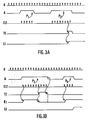
- the signal at point A changes to a determined logic state, for example state 1.
- This operating mode is shown in FIG. 3A.
- the AND gate 14 (FIG. 1) delivers a signal CL1 which serves as a clock for a counter 12.
- CL1 which serves as a clock for a counter 12.
- the latter is previously loaded with a set value M defining the predetermined duration.
- M has been programmed for a duration of seven clock ticks, the passage from A to state 0 before a duration less than seven clock clocks (case P1) will not cause any change in the TC output of the counter.
- the signal present on this channel appears at point A.
- the event to be detected causes a signal to appear in A in logic state 1 (FIG. 3B).
- the clock CL1 goes to logic state 1 and triggers the start of counting of counter 12 which has previously been loaded with the set value M.
- the signal CL1 also activates a input of an R / S flip-flop 13 and puts its output Q1 in logic state 1. If the counter reaches the setpoint value M (for example 7 clock ticks) before signal A changes logic state ( case P3) then the output TC switches the output Q1 of flip-flop 13 of type R / S to logic state 0. When the falling edge of signal A appears, it validates in flip-flop 16 of type D the signal Q1 which is copied according to S2 according to a logic state 0.
- the multiplexer 17 can select the vertical mode or the horizontal mode using the signal SEL and deliver the trigger signal. This selection is preferably made by programming the passage of the SEL signal in order to be able to observe the two operating modes successively.
- FIG. 2 represents the selector 10 of the channels 1, 2 ... N.
- the input bus 11 arrives on logic gates operating the reverse exclusive OR function 201 ... 20 N. These doors receive the reference combination C. Their outputs are joined to logic gates 211, 212 ... 21 N operating the NOR function. These doors receive the reference combination B. Their outputs are combined with one or more logic doors, in the example a NOR gate. In vertical release, combination B validates all doors 211 to 21 N. When the input combination is identical to the reference combination C, output A changes to logic state 1.
Landscapes
- Engineering & Computer Science (AREA)
- General Engineering & Computer Science (AREA)
- Physics & Mathematics (AREA)
- General Physics & Mathematics (AREA)
- Theoretical Computer Science (AREA)
- Computer Hardware Design (AREA)
- Quality & Reliability (AREA)
- Test And Diagnosis Of Digital Computers (AREA)
Claims (4)
- Logikanalysator mit:- einem Kanal-Wähler (10) mit ersten Eingängen (11) zum Empfang einer Zusammensetzung digitaler Signale, mit zweiten Eingängen zum Empfangen einer ersten Bezugskombination (C) digitaler Signale zu einem gegebenen Zeitpunkt und mit ersten Logikgattern (20₁-20N) zum Detektieren, entsprechend einer ersten Betriebsart, daß die erste Kombination (C) auf den ersten Eingängen reproduziert worden ist,- einem Zähler (12), gesteuert von einem Takt (CL1), der von dem Ausgang des Wählers (10) freigegeben wird, wobei der Ausgang des Wählers auch den Zähler startet, der zuvor einen ersten Einstellwert (M) empfängt, der eine erste vorbestimmte Dauer definiert,- einem ersten Speichermittel (15), das ein erstes Freigabesignal (S1) speichert und abgibt, das aktiv ist, wenn die erste Kombination (C) über die erste genannte Dauer hinaus reproduziert bleibt, wobei das erste Speichermittel von dem Zähler (12) aktiviert wird,
dadurch gekennzeichnet, daß- der Wähler (10) dritte Eingänge hat zum Empfangen einer zweiten Bezugskombination (B) und zweite Logikgatter (21₁ - 21N) zum Wählen, entsprechend einer zweiten Betriebsart, eines Kanals der ersten Eingänge (11), auf dem in der Zusammensetzung digitaler Signale ein Auftreten einer Folge identischer Bits detektiert worden ist,- der Zähler (12) zuvor einen zweiten Einstellwert (M) empfängt, der eine zweite vorgegebene Dauer definiert, wobei der Zähler vom Ausgang des genannten Wählers (10) gestartet wird,- zweite Speichermittel (13, 16) detektieren, wenn das Auftreten der Folge identischer Bits auf dem gewählten Kanal kürzer als die zweite vorbestimmte Dauer ist, und in diesem Fall ein zweites Freigabesignal (S2) speichern und abgeben,- der Wähler (10) am Eingang die erste oder zweite Betriebsart wählt, je nachdem, ob die zweite Bezugskombination (B) alle Kanäle oder einen einzigen Kanal wählt,- ein Multiplexer (17) am Ausgang eines der Freigabesignale (S1, S2) mit Hilfe eines Triggerungsartsignals (SEL) wählt. - Logikanalysator nach Anspruch 1, dadurch gekennzeichnet, daß der Wähler (10), um auf N Kanälen zu arbeiten, für jeden Kanal folgendes umfaßt: ein genanntes erstes Logikgatter, das einen Kanal und eines der N Bits der ersten Bezugskombination (C) empfängt, wobei der Ausgang dieses ersten Logikgatters mit dem Eingang eines zweiten Logikgatters verbunden ist, das ebenfalls eines der N Bits der zweiten Bezugskombination (B) empfängt, wobei die erste Bezugskombination (C) ein beliebiges Binärwort selektieren soll, die zweite Bezugskombination (B) einen der N Kanäle oder alle N Kanäle wählen soll, um die Kanalsteuerung zu bilden, wobei die Ausgänge der jedem Kanal zugeordneten zweiten Logikgatter mit einem Logikgatter verbunden sind, das für alle Ausgänge die logische UND-Verknüpfung ausführt, um das Ausgangssignal (A) des Wählers (10) zu liefern.
- Logikanalysator nach Anspruch 1 oder 2, dadurch gekennzeichnet, daß das erste Speichermittel aus einem Flipflop (15) besteht, das die Ausgabe des Wählers (10) speichert.
- Logikanalysator nach einem der Ansprüche 1 bis 3, dadurch gekennzeich net, daß die zweiten Speichermittel aus einem R/S-Flipflop (13) bestehen, dem ein D-Flipflop (16) folgt.
Applications Claiming Priority (2)
| Application Number | Priority Date | Filing Date | Title |
|---|---|---|---|
| FR8814423A FR2638865B1 (fr) | 1988-11-04 | 1988-11-04 | Analyseur logique avec double declenchement |
| FR8814423 | 1988-11-04 |
Publications (2)
| Publication Number | Publication Date |
|---|---|
| EP0367345A1 EP0367345A1 (de) | 1990-05-09 |
| EP0367345B1 true EP0367345B1 (de) | 1995-09-06 |
Family
ID=9371584
Family Applications (1)
| Application Number | Title | Priority Date | Filing Date |
|---|---|---|---|
| EP89202727A Expired - Lifetime EP0367345B1 (de) | 1988-11-04 | 1989-10-30 | Logikanalysator mit Doppel-Triggerung |
Country Status (5)
| Country | Link |
|---|---|
| US (1) | US5031128A (de) |
| EP (1) | EP0367345B1 (de) |
| JP (1) | JPH02181660A (de) |
| DE (1) | DE68924125T2 (de) |
| FR (1) | FR2638865B1 (de) |
Families Citing this family (11)
| Publication number | Priority date | Publication date | Assignee | Title |
|---|---|---|---|---|
| KR100266691B1 (ko) * | 1998-05-25 | 2000-09-15 | 김영환 | 홀드/리셋 모드 선택 카운터 및 그 실행방법 |
| US6396517B1 (en) | 1999-03-01 | 2002-05-28 | Agilent Technologies, Inc. | Integrated trigger function display system and methodology for trigger definition development in a signal measurement system having a graphical user interface |
| US6327544B1 (en) * | 1999-03-01 | 2001-12-04 | Agilent Technologies, Inc. | Automatic storage of a trigger definition in a signal measurement system |
| JP4408193B2 (ja) * | 2002-08-08 | 2010-02-03 | 富士通マイクロエレクトロニクス株式会社 | 半導体記憶装置及び半導体記憶装置の試験方法 |
| JP5123150B2 (ja) * | 2008-12-10 | 2013-01-16 | 株式会社東芝 | トリガー信号検出装置 |
| US8531209B2 (en) * | 2009-01-16 | 2013-09-10 | Tektronix, Inc. | Multifunction word recognizer element |
| US8332697B1 (en) * | 2010-07-20 | 2012-12-11 | Xilinx, Inc. | Method and apparatus for triggering and capturing digital circuit signals |
| US8533518B2 (en) | 2011-01-07 | 2013-09-10 | Anue Systems, Inc. | Systems and methods for precise timing measurements using high-speed deserializers |
| US8850259B2 (en) | 2011-01-07 | 2014-09-30 | Anue Systems, Inc. | Systems and methods for precise generation of phase variation in digital signals |
| US8683254B2 (en) | 2011-01-07 | 2014-03-25 | Anue Systems, Inc. | Systems and methods for precise event timing measurements |
| US8788867B2 (en) | 2011-01-07 | 2014-07-22 | Anue Systems, Inc. | Systems and methods for playback of detected timing events |
Family Cites Families (7)
| Publication number | Priority date | Publication date | Assignee | Title |
|---|---|---|---|---|
| US3760355A (en) * | 1972-03-08 | 1973-09-18 | Motorola Inc | Digital pattern detector |
| JPS6039189B2 (ja) * | 1979-05-23 | 1985-09-04 | テクトロニツクス・インコ−ポレイテツド | 信号測定装置 |
| US4404542A (en) * | 1980-12-05 | 1983-09-13 | Rca Corporation | Digital sequence detector |
| EP0166274A3 (de) * | 1984-06-04 | 1988-09-14 | Siemens Aktiengesellschaft | Schaltungsanordnung zum Ermitteln bestimmter Bitmuster in seriell auftretenden binären Signalen |
| US4829462A (en) * | 1986-06-13 | 1989-05-09 | International Business Machines Corporation | Communication bit pattern detection circuit |
| US4774438A (en) * | 1986-09-05 | 1988-09-27 | Tektronix, Inc. | Oscilloscope trace attribute control system |
| US4847877A (en) * | 1986-11-28 | 1989-07-11 | International Business Machines Corporation | Method and apparatus for detecting a predetermined bit pattern within a serial bit stream |
-
1988
- 1988-11-04 FR FR8814423A patent/FR2638865B1/fr not_active Expired - Lifetime
-
1989
- 1989-10-30 DE DE68924125T patent/DE68924125T2/de not_active Expired - Fee Related
- 1989-10-30 EP EP89202727A patent/EP0367345B1/de not_active Expired - Lifetime
- 1989-11-02 JP JP1285112A patent/JPH02181660A/ja active Pending
- 1989-11-06 US US07/433,062 patent/US5031128A/en not_active Expired - Fee Related
Non-Patent Citations (2)
| Title |
|---|
| Computer design mars 1981, pages 119-126, P.Dittman et al.: Logic analyzers simplify system integration tasks, pages 121,122, figure 2C * |
| Electronique industrielle no. 112, 15 septembre 1986, pages 55-63, Paris, F.B.COMBY: " L'interet d'une acquisition en temporel transitionell en analyse logique radipe", page 59 paragraphe: " Une double analyse permet des mesures couplees", page 60; figure 11 * |
Also Published As
| Publication number | Publication date |
|---|---|
| EP0367345A1 (de) | 1990-05-09 |
| DE68924125D1 (de) | 1995-10-12 |
| FR2638865B1 (fr) | 1990-12-28 |
| US5031128A (en) | 1991-07-09 |
| FR2638865A1 (fr) | 1990-05-11 |
| JPH02181660A (ja) | 1990-07-16 |
| DE68924125T2 (de) | 1996-04-18 |
Similar Documents
| Publication | Publication Date | Title |
|---|---|---|
| EP0683454B1 (de) | Verfahren zur Überwachung des Programmablaufs | |
| FR2626120A1 (fr) | Generateur d'impulsions en correlation | |
| EP0578540B1 (de) | Verfahren zur Prüfung der Funktionsfähigkeit einer ASIC-Schaltung und darauf bezogene ASIC-Schaltung | |
| EP0367345A1 (de) | Logikanalysator mit Doppel-Triggerung | |
| EP0051019B1 (de) | Zählvorrichtung für Hochfrequenzimpulse | |
| EP0490738B1 (de) | Integrierter Schaltkreis mit Peripherieprüfungssteuerung | |
| BE897587A (fr) | Circuit parallele de controle de redondance cyclique | |
| FR2579817A1 (fr) | Dispositif pour verifier des cellules de memoire en fonction de l'etat de seuil pouvant etre obtenu en phase d'ecriture | |
| FR2494868A1 (fr) | Circuit logique permettant une operation d'essai | |
| EP0833346B1 (de) | Serieller Zugriffsspeicher mit Schreibsicherung | |
| EP0013341A1 (de) | System zur Zeitkompression von Sprachsignalen | |
| EP0058108B1 (de) | Generator für kombinierte logische Signale | |
| EP0632279A1 (de) | Apparat zur Messung der Dauer eines Zeitintervalls | |
| EP0464768B1 (de) | Schnittstellenmodul für Datenübertragung | |
| FR2474722A1 (fr) | Dispositif de determination numerique de correlation d'images | |
| FR2808333A1 (fr) | Procede et appareil de calibrage pour corriger des erreurs de synchronisation de largeur d'impulsion lors de tests de circuits integres | |
| FR2632733A1 (fr) | Suiveur d'echo pour appareil de mesure par ultrasons de la position d'une paroi mobile | |
| EP0526359A1 (de) | Verfahren und Schaltungsanordnung zur Synchronisierung eines Signals | |
| FR3047136A1 (de) | ||
| FR2810438A1 (fr) | Circuit de detection d'usure | |
| EP0640910B1 (de) | Verfahren zur Steuerung einer FIFO-Schaltung und Einrichtung zu seiner Durchführung | |
| EP0408439A1 (de) | Signalgenerator für programmierbare logische Zustände | |
| EP3189379A2 (de) | Aufpralldetektionsschaltung | |
| EP0881768A1 (de) | System und Verfahren zur Filterung eines Impulssignals | |
| FR2889328A1 (fr) | Dispositif d'interfacage unidirectionnel de type fifo entre un bloc maitre et un bloc esclave, bloc maitre et bloc esclave correspondants |
Legal Events
| Date | Code | Title | Description |
|---|---|---|---|
| PUAI | Public reference made under article 153(3) epc to a published international application that has entered the european phase |
Free format text: ORIGINAL CODE: 0009012 |
|
| AK | Designated contracting states |
Kind code of ref document: A1 Designated state(s): CH DE FR GB IT LI NL SE |
|
| 17P | Request for examination filed |
Effective date: 19901107 |
|
| 17Q | First examination report despatched |
Effective date: 19920729 |
|
| GRAA | (expected) grant |
Free format text: ORIGINAL CODE: 0009210 |
|
| AK | Designated contracting states |
Kind code of ref document: B1 Designated state(s): CH DE FR GB IT LI NL SE |
|
| PG25 | Lapsed in a contracting state [announced via postgrant information from national office to epo] |
Ref country code: IT Free format text: LAPSE BECAUSE OF FAILURE TO SUBMIT A TRANSLATION OF THE DESCRIPTION OR TO PAY THE FEE WITHIN THE PRE;WARNING: LAPSES OF ITALIAN PATENTS WITH EFFECTIVE DATE BEFORE 2007 MAY HAVE OCCURRED AT ANY TIME BEFORE 2007. THE CORRECT EFFECTIVE DATE MAY BE DIFFERENT FROM THE ONE RECORDED.SCRIBED TIME-LIMIT Effective date: 19950906 Ref country code: NL Free format text: LAPSE BECAUSE OF NON-PAYMENT OF DUE FEES Effective date: 19950906 |
|
| REF | Corresponds to: |
Ref document number: 68924125 Country of ref document: DE Date of ref document: 19951012 |
|
| PG25 | Lapsed in a contracting state [announced via postgrant information from national office to epo] |
Ref country code: LI Effective date: 19951031 Ref country code: CH Effective date: 19951031 |
|
| PG25 | Lapsed in a contracting state [announced via postgrant information from national office to epo] |
Ref country code: SE Effective date: 19951206 |
|
| GBT | Gb: translation of ep patent filed (gb section 77(6)(a)/1977) |
Effective date: 19951212 |
|
| NLV1 | Nl: lapsed or annulled due to failure to fulfill the requirements of art. 29p and 29m of the patents act | ||
| REG | Reference to a national code |
Ref country code: FR Ref legal event code: CJ Ref country code: FR Ref legal event code: CD |
|
| REG | Reference to a national code |
Ref country code: CH Ref legal event code: PL |
|
| PLBE | No opposition filed within time limit |
Free format text: ORIGINAL CODE: 0009261 |
|
| STAA | Information on the status of an ep patent application or granted ep patent |
Free format text: STATUS: NO OPPOSITION FILED WITHIN TIME LIMIT |
|
| 26N | No opposition filed | ||
| PGFP | Annual fee paid to national office [announced via postgrant information from national office to epo] |
Ref country code: GB Payment date: 19960930 Year of fee payment: 8 |
|
| PGFP | Annual fee paid to national office [announced via postgrant information from national office to epo] |
Ref country code: FR Payment date: 19961022 Year of fee payment: 8 |
|
| PGFP | Annual fee paid to national office [announced via postgrant information from national office to epo] |
Ref country code: DE Payment date: 19961218 Year of fee payment: 8 |
|
| PG25 | Lapsed in a contracting state [announced via postgrant information from national office to epo] |
Ref country code: GB Free format text: LAPSE BECAUSE OF NON-PAYMENT OF DUE FEES Effective date: 19971030 |
|
| PG25 | Lapsed in a contracting state [announced via postgrant information from national office to epo] |
Ref country code: FR Free format text: THE PATENT HAS BEEN ANNULLED BY A DECISION OF A NATIONAL AUTHORITY Effective date: 19971031 |
|
| GBPC | Gb: european patent ceased through non-payment of renewal fee |
Effective date: 19971030 |
|
| PG25 | Lapsed in a contracting state [announced via postgrant information from national office to epo] |
Ref country code: DE Free format text: LAPSE BECAUSE OF NON-PAYMENT OF DUE FEES Effective date: 19980701 |
|
| REG | Reference to a national code |
Ref country code: FR Ref legal event code: ST |