EP0368584A2 - Méthode de fabrication d'une tranche semi-conducteur - Google Patents
Méthode de fabrication d'une tranche semi-conducteur Download PDFInfo
- Publication number
- EP0368584A2 EP0368584A2 EP89311454A EP89311454A EP0368584A2 EP 0368584 A2 EP0368584 A2 EP 0368584A2 EP 89311454 A EP89311454 A EP 89311454A EP 89311454 A EP89311454 A EP 89311454A EP 0368584 A2 EP0368584 A2 EP 0368584A2
- Authority
- EP
- European Patent Office
- Prior art keywords
- semiconductor
- stopper
- semiconductor layer
- layer
- polishing
- Prior art date
- Legal status (The legal status is an assumption and is not a legal conclusion. Google has not performed a legal analysis and makes no representation as to the accuracy of the status listed.)
- Granted
Links
Images



Classifications
-
- H—ELECTRICITY
- H10—SEMICONDUCTOR DEVICES; ELECTRIC SOLID-STATE DEVICES NOT OTHERWISE PROVIDED FOR
- H10P—GENERIC PROCESSES OR APPARATUS FOR THE MANUFACTURE OR TREATMENT OF DEVICES COVERED BY CLASS H10
- H10P90/00—Preparation of wafers not covered by a single main group of this subclass, e.g. wafer reinforcement
- H10P90/12—Preparing bulk and homogeneous wafers
- H10P90/129—Preparing bulk and homogeneous wafers by polishing
-
- H—ELECTRICITY
- H10—SEMICONDUCTOR DEVICES; ELECTRIC SOLID-STATE DEVICES NOT OTHERWISE PROVIDED FOR
- H10D—INORGANIC ELECTRIC SEMICONDUCTOR DEVICES
- H10D30/00—Field-effect transistors [FET]
- H10D30/01—Manufacture or treatment
- H10D30/014—Manufacture or treatment of FETs having zero-dimensional [0D] or one-dimensional [1D] channels, e.g. quantum wire FETs, single-electron transistors [SET] or Coulomb blockade transistors
-
- B—PERFORMING OPERATIONS; TRANSPORTING
- B82—NANOTECHNOLOGY
- B82Y—SPECIFIC USES OR APPLICATIONS OF NANOSTRUCTURES; MEASUREMENT OR ANALYSIS OF NANOSTRUCTURES; MANUFACTURE OR TREATMENT OF NANOSTRUCTURES
- B82Y10/00—Nanotechnology for information processing, storage or transmission, e.g. quantum computing or single electron logic
-
- H—ELECTRICITY
- H10—SEMICONDUCTOR DEVICES; ELECTRIC SOLID-STATE DEVICES NOT OTHERWISE PROVIDED FOR
- H10P—GENERIC PROCESSES OR APPARATUS FOR THE MANUFACTURE OR TREATMENT OF DEVICES COVERED BY CLASS H10
- H10P54/00—Cutting or separating of wafers, substrates or parts of devices
-
- H—ELECTRICITY
- H10—SEMICONDUCTOR DEVICES; ELECTRIC SOLID-STATE DEVICES NOT OTHERWISE PROVIDED FOR
- H10P—GENERIC PROCESSES OR APPARATUS FOR THE MANUFACTURE OR TREATMENT OF DEVICES COVERED BY CLASS H10
- H10P90/00—Preparation of wafers not covered by a single main group of this subclass, e.g. wafer reinforcement
- H10P90/19—Preparing inhomogeneous wafers
- H10P90/1904—Preparing vertically inhomogeneous wafers
- H10P90/1906—Preparing SOI wafers
- H10P90/1914—Preparing SOI wafers using bonding
-
- H—ELECTRICITY
- H10—SEMICONDUCTOR DEVICES; ELECTRIC SOLID-STATE DEVICES NOT OTHERWISE PROVIDED FOR
- H10P—GENERIC PROCESSES OR APPARATUS FOR THE MANUFACTURE OR TREATMENT OF DEVICES COVERED BY CLASS H10
- H10P95/00—Generic processes or apparatus for manufacture or treatments not covered by the other groups of this subclass
- H10P95/06—Planarisation of inorganic insulating materials
- H10P95/062—Planarisation of inorganic insulating materials involving a dielectric removal step
-
- H—ELECTRICITY
- H10—SEMICONDUCTOR DEVICES; ELECTRIC SOLID-STATE DEVICES NOT OTHERWISE PROVIDED FOR
- H10W—GENERIC PACKAGES, INTERCONNECTIONS, CONNECTORS OR OTHER CONSTRUCTIONAL DETAILS OF DEVICES COVERED BY CLASS H10
- H10W10/00—Isolation regions in semiconductor bodies between components of integrated devices
- H10W10/10—Isolation regions comprising dielectric materials
- H10W10/181—Semiconductor-on-insulator [SOI] isolation regions, e.g. buried oxide regions of SOI wafers
-
- H—ELECTRICITY
- H10—SEMICONDUCTOR DEVICES; ELECTRIC SOLID-STATE DEVICES NOT OTHERWISE PROVIDED FOR
- H10D—INORGANIC ELECTRIC SEMICONDUCTOR DEVICES
- H10D30/00—Field-effect transistors [FET]
- H10D30/40—FETs having zero-dimensional [0D], one-dimensional [1D] or two-dimensional [2D] charge carrier gas channels
- H10D30/43—FETs having zero-dimensional [0D], one-dimensional [1D] or two-dimensional [2D] charge carrier gas channels having one-dimensional [1D] charge carrier gas channels, e.g. quantum wire FETs or transistors having 1D quantum-confined channels
-
- Y—GENERAL TAGGING OF NEW TECHNOLOGICAL DEVELOPMENTS; GENERAL TAGGING OF CROSS-SECTIONAL TECHNOLOGIES SPANNING OVER SEVERAL SECTIONS OF THE IPC; TECHNICAL SUBJECTS COVERED BY FORMER USPC CROSS-REFERENCE ART COLLECTIONS [XRACs] AND DIGESTS
- Y10—TECHNICAL SUBJECTS COVERED BY FORMER USPC
- Y10S—TECHNICAL SUBJECTS COVERED BY FORMER USPC CROSS-REFERENCE ART COLLECTIONS [XRACs] AND DIGESTS
- Y10S148/00—Metal treatment
- Y10S148/012—Bonding, e.g. electrostatic for strain gauges
-
- Y—GENERAL TAGGING OF NEW TECHNOLOGICAL DEVELOPMENTS; GENERAL TAGGING OF CROSS-SECTIONAL TECHNOLOGIES SPANNING OVER SEVERAL SECTIONS OF THE IPC; TECHNICAL SUBJECTS COVERED BY FORMER USPC CROSS-REFERENCE ART COLLECTIONS [XRACs] AND DIGESTS
- Y10—TECHNICAL SUBJECTS COVERED BY FORMER USPC
- Y10S—TECHNICAL SUBJECTS COVERED BY FORMER USPC CROSS-REFERENCE ART COLLECTIONS [XRACs] AND DIGESTS
- Y10S148/00—Metal treatment
- Y10S148/135—Removal of substrate
-
- Y—GENERAL TAGGING OF NEW TECHNOLOGICAL DEVELOPMENTS; GENERAL TAGGING OF CROSS-SECTIONAL TECHNOLOGIES SPANNING OVER SEVERAL SECTIONS OF THE IPC; TECHNICAL SUBJECTS COVERED BY FORMER USPC CROSS-REFERENCE ART COLLECTIONS [XRACs] AND DIGESTS
- Y10—TECHNICAL SUBJECTS COVERED BY FORMER USPC
- Y10S—TECHNICAL SUBJECTS COVERED BY FORMER USPC CROSS-REFERENCE ART COLLECTIONS [XRACs] AND DIGESTS
- Y10S438/00—Semiconductor device manufacturing: process
- Y10S438/97—Specified etch stop material
-
- Y—GENERAL TAGGING OF NEW TECHNOLOGICAL DEVELOPMENTS; GENERAL TAGGING OF CROSS-SECTIONAL TECHNOLOGIES SPANNING OVER SEVERAL SECTIONS OF THE IPC; TECHNICAL SUBJECTS COVERED BY FORMER USPC CROSS-REFERENCE ART COLLECTIONS [XRACs] AND DIGESTS
- Y10—TECHNICAL SUBJECTS COVERED BY FORMER USPC
- Y10S—TECHNICAL SUBJECTS COVERED BY FORMER USPC CROSS-REFERENCE ART COLLECTIONS [XRACs] AND DIGESTS
- Y10S438/00—Semiconductor device manufacturing: process
- Y10S438/977—Thinning or removal of substrate
Definitions
- the present invention relates to a method of manufacturing a semiconductor wafer and, more particularly, to a novel method adapted to manufacture a highly flat semiconductor wafer having a uniform thickness.
- the present invention relates also to a semiconductor device and a method of manufacturing the same, and more particularly to those optimal for application to a semiconductor device of a quantum well wire structure.
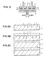
- FIG. 3 (A) through (D) are sectional views illustrating the sequential steps in such manufacturing method mentioned.
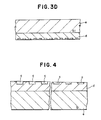
- the semiconductor layers c, c ... are prone to become nonuniform in thickness as shown in Fig. 4. Since the silicon semiconductor wafer has a size of 4 to 8 inches, some thickness variation of 1 to 2 microns may occur if the silicon semiconductor wafer of such dimensions is polished to a depth of 600 microns or so. Consequently, as illustrated in the left-hand area of Fig. 4, the semiconductor layers c, c ... become excessively thicker to be connected eventually to one another through silicon. Meanwhile in some other portions, the semiconductor layers c, c ... become thinner as illustrated in the right-hand area of Fig. 4.
- the silicon dioxide layer d serving as a stopper is somewhat polished to be thinner.
- the yield rate is deteriorated in the production to consequently bring about nonnegligible impediment in realizing low-cost production of IC, LSI, VLSI and so forth.
- a quantum well wire is so fine that sectional dimensions Lx and Ly thereof are substantially equivalent to the de Broglie wavelength ⁇ e (e.g. 200 angstroms) of electron.
- ⁇ e de Broglie wavelength
- the motions of electrons are quantized in the x- and y-directions, so that the electron motions are permitted merely in the longitudinal direction along the well wire, i.e. in the z-direction alone. Consequently the electrons are rendered one-dimensional.
- the entire electrons are within the ground level and the elastic scattering thereof is suppressed, so that its application is expected with regard to a field effect transistor (FET) where the electron mobility is high.
- FET field effect transistor
- the dimension Lx is not increasable beyond 2000 angstroms due to the restriction concerning the lithography, thereby bringing about difficulties in producing a silicon MOSFET of a quantum well wire structure.
- Another object of the invention resides in providing an improved semiconductor device adapted to realize a quantum well wire structure.
- a further object of the invention is to provide a method of manufacturing a semiconductor device of a quantum well wire structure with high precision.
- the present invention is so contrived as to attain a high uniformity in the thickness of a semiconductor layer by first forming hardly polishable stoppers of mutually different thicknesses in the semiconductor, then polishing the semiconductor until the thicker stopper is exposed on one main surface of the semiconductor, subsequently removing the thicker stopper to attain a thickness less than that of the thinner stopper, and thereafter polishing the aforesaid one main surface of the semiconductor until the thinner stopper is exposed.
- the semiconductor device of the present invention comprises a semiconductor layer formed on an insulator substrate, a thermally oxidized film of the semiconductor layer formed on such layer, and a gate electrode formed on one side of the semiconductor layer, wherein the channel width is determined by the thickness of the semiconductor layer. According to such constitution, it becomes possible to realize a semiconductor device of a quantum well wire structure.
- the semiconductor device manufacturing method of the invention comprises a step of forming a thin film by thermally oxidizing a semiconductor layer on an insulator substrate; a step of selectively removing the thin-film semiconductor layer; and a step of forming a gate electrode on one side of the semiconductor layer removed selectively.
- the above method is capable of producing a semiconductor device of a quantum well wire structure with high precision.
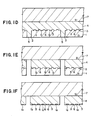
- FIGs. 1 and 2 illustrate an exemplary embodiment contrived to carry out the semiconductor wafer manufacturing method of the invention, in which Fig. 1 (A) through (F) are sectional views representing the sequential steps of such method.
- Fig. 2 is a schematic sectional view of an exemplary polishing apparatus including a level block 8; heads 9, 9; mount plates 10, 10 attached to the heads 9, 9; and a wax 11 through which a semiconductor wafer W to be polished is secured to the mount plate 10. And a polishing operation is performed by moving the semiconductor wafer W relatively to the level block 8 by means of the heads 9, 9 in a state where an abrasive material 12 is interposed between the surface of the semiconductor wafer W to be polished and the level block 8.
- One of preferred abrasive materials is obtained by dispersing fine particles (e.g. 0.02 micron or so in particle size) of high-purity quartz into an alkaline solution of pH 10 to 11.
- the abrasive material 12 is dripped onto the level block 8 while the semiconductor wafer W is rotated with a slight gap maintained to the level block 8. It is also permitted of course to adopt the known polishing method which performs the operation while keeping a polishing cloth in contact with the surface of the semiconductor wafer W. However, according to such conventional method, there exists the possibility that the polishing cloth may be compressed and deformed along the surface of the semiconductor wafer W. Consequently the polishing with an abrasive material is considered superior.
- the polishing after joining the semiconductor wafers together is executed in two stages.
- the first polishing stage the first stopper 5 positioned in the scribe region is used as a stopper to achieve macroscopic flattening.
- thickness variation of the first stoppers 5 caused to the polishing corresponds to thickness variation of the semiconductor wafer substan tially directly, and such variation ranges from 1 to 2 microns in the entire wafer.
- the first stopper 5 is so removed that its thickness becomes equal to or smaller than that of the second stopper 6, and then another polishing operation is performed while using the second stopper 6, whereby the thickness variation relative to the first stopper 5 is eliminated to nil.
- the semiconductor wafer manufacturing method of the present invention comprises a step of forming, in a semiconductor, at least a first stopper of a hardly polishable material and a second stopper thinner than the first stopper, a step of polishing the semiconductor until the first stopper is exposed, a step of removing the first stopper until the same becomes equal in thickness to the second stopper, and a step of polishing the semiconductor until the second stopper is exposed.
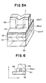
- Fig. 5A through 5H illustrate the sequential steps of a method for manufacture of a silicon MOSFET according to this embodiment.
- selective etching is first performed by a process of reactive ion etching (RIE) on one main surface of a monocrystal p-type silicon substrate 51 thereby forming recesses of 1000 angstroms or so in depth. Then the surface of the p-type silicon substrate 51 is thermally oxidized to form a silicon dioxide (SiO2) film (not shown), and thereafter this film is removed by etching to eliminate the crystal defect caused in the surface layer of the p-type silicon substrate 51 by the preceding RIE. Subsequently a silicon dioxide film 52, for example, is formed on the entire surface by a process of CVD (chemical vapor deposition) or thermal oxidation.
- CVD chemical vapor deposition
- the aforementioned p-type silicon substrate 51 is mounted on the silicon substrate 53 in such a manner that the silicon dioxide film 52 is retained in contact with the silicon dioxide film54, and in the presence of an oxygen atmosphere or the like, heat treatment is executed at a high temperature of, e.g. 100°C to join the two silicon substrates 51 and 53 together.
- the p-type silicon substrate 51 is ground until the silicon dioxide film 52 formed at the bottom of the recess 51a is exposed from the other main surface of the substrate 51, whereby a monocrystal p-type silicon layer 55 of 1000 angstroms or so in depth is formed in the shape of an island as shown in Fig. 5C.
- the p-type silicon layer 55 is formed on the silicon dioxide films 52,54 in the so-called SOI (silicon on insulator) structure.
- SOI silicon on insulator
- the lapping is performed until the height of the silicon dioxide film 52formed at the bottom of the recess 51a becomes about 2 microns from the film surface, and thereafter the polishing is performed.
- the high-hardness silicon dioxide film 52 serves as a stopper to automatically halt the polishing upon exposure of the silicon dioxide film 52.
- the aforementioned p-type silicon layer 55 is thermally oxidized to form a silicon dioxide film 56 having a thickness of 1400 angstroms or so, whereby the p-type silicon layer 55 is partially shaped into a thin film of about 300 angstroms in thickness.
- a resist pattern 57 having a predetermined contour is formed by lithography, and then the silicon dioxide film 56 and the p-type silicon layer 55 are anisotropically etched by RIE process or the like in the direction perpendicular to the substrate surface with the resist pattern 57 used as a mask, thereby forming a rectangular opening 58.
- Such etching may be terminated upon exposure of the silicon dioxide film 52, or over-etching may be performed to a depth indicated by, for example, a one-dot chain line.
- the p- type silicon layer 55 is thermally oxidized again to form, as shown in Fig. 5F, a gate silicon dioxide film 59 of about 200 angstroms in thickness on one side of the p-type silicon layer 55 exposed below the two sides of the opening 58, and simultaneously such p-type silicon layer 55 is partially shaped into a thin film of about 200 angstroms in thickness.
- a gate electrode film 60 composed of polycrystal silicon, aluminum or the like is formed on the entire surface.
- a resist pattern (not shown) having a predetermined contour is formed on the gate electrode film 60, and both the film 60 thus obtained and the silicon dioxide film 56 are etched in succession anisotropically by RIE process or the like with the resist pattern used as a mask, whereby a gate electrode 61 is formed as shown in Fig. 5H.
- an n-type impurity such as arsenic (As) is ion-implanted at a high concentration into the p-type silicon layer 55 exposed on the two sides of the gate electrode 61 by the etching, so that an n+-type source region 62 and an n+-type drain region 63 are formed in a self-matched state with respect to the gate electrode 61.
- a source region 62 and a drain region 63 by ion-implanting an n-type impurity in a state where the silicon dioxide film 56 having a thickness of several hundred angstroms is left on the p-type silicon layer 55, instead of etching the silicon dioxide film 56 so deep as to expose the p-type silicon layer 55.
- an n-type inverse layer (channel) 64 is formed, by applying a gate voltage to the gate electrode 61, in the p-type silicon layer 55 proximate to the interface between the gate silicon dioxide film 59 and the p-type silicon layer 55, as shown in Fig. 6.
- the n-type inverse layer 64 is formed on each of the two sides of the p-type silicon layer 55.
- Such n-type inverse layer 64 has an effective thickness of 100 angstroms or so.
- the vertical dimension of the n-type inverse layer 64, i.e. the channel width thereof, is equivalent to the thickness of the p-type silicon layer 55 and is therefore 200 angstroms or so.
- the sectional dimensions Lx and Ly of the n-type inverse layer 64 become substantially equivalent to the de Broglie wavelength ⁇ e, so that a quantum well wire is composed of such n-type inverse layer (channel) 64.
- the p-type silicon layer 55 formed on the silicon dioxide film 52 is thermally oxidized to shape a thin film of about 300 angstroms in thickness, and then a gate silicon dioxide film 59 is formed on one side of the p-type silicon layer 55 by thermal oxidation. And simultaneously the p-type silicon layer 55 is shaped into a thin film having a thickness of about 200 angstroms, thereby forming a MOS structure where the channel width is substantially equivalent to the de Broglie wavelength ⁇ e.
- a silicon MOSFET of a quantum well wire structure can be manufactured with high precision despite the restriction concerning the lithography.
- the silicon MOSFET of such quantum well wire structure is capable of performing an ultrahigh-speed operation.
- the p-type silicon layer 55 is formed in a recess shaped in the silicon dioxide film 52, it is isolated with complete insulation to consequently attain perfect separation between silicon MOSFETs when integrating a plurality of such FETs.
- the invention is applicable also to, e.g. a Schottky gate FET.
- a Schottky gate FET e.g. a Schottky gate FET.
- an n-type silicon layer is used in place of the p-type silicon layer 5 and, similarly to the aforementioned embodiment, such n-type silicon layer is partially shaped into a thin film of several hundred angstroms in thickness.
- a Schottky gate electrode is formed directly on one side of the n-type silicon layer.
- the transverse dimension Lx of the n-type silicon layer needs to be reduced substantially to the de Broglie wavelength ⁇ e. This condition can be achieved by reducing, through thermal oxidation, the transverse dimension of the n-type silicon layer after forming the opening 58.
- AB effect transistor a transistor utilizing Aharonov-Bohm effect
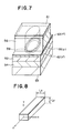
- Fig. 7 shows an example of such AB effect transistor.
- the rectangular opening 58 in the above embodiment may be modified in shape to a scaphoid, and the gate silicon dioxide film 59 may be formed on one side of the p-type silicon layer 55 exposed to such scaphoid opening 58. It is preferred in this case that the dimensions of the junction among the source region 62, the drain region 63 and the n-type inverse layers 64 formed on the two sides of the p-type silicon layer 55 be substantially equal to or less than the de Broglie wavelength ⁇ e.
- the electron waves emitted from the source region 62 are divided into two currents which pass through two n-type inverse layers 64 formed on the two sides of the p-type silicon layer 55, and thereafter such two electron currents join again in the drain region 63. In this stage, there occurs interference of the electron waves. Then a magnetic field is applied in the direction perpendicular to the substrate surface in a state where the n-type inverse layer 64 is formed by impressing a gate voltage to the gate electrode 61, and the phase difference between the two electron currents passing through the n-type inverse layers 14 is controlled by the magnetic field thus applied, thereby performing a transistor operation. According to this example, an AB effect transistor can be realized with facility.
- the invention is adapted to manufacture an improved semiconductor device of a quantum well wire structure with high precision.
- the invention is capable of achieving complete isolation of the semiconductor layer with perfect insulation.
Landscapes
- Engineering & Computer Science (AREA)
- Chemical & Material Sciences (AREA)
- Nanotechnology (AREA)
- Physics & Mathematics (AREA)
- Mathematical Physics (AREA)
- Theoretical Computer Science (AREA)
- Crystallography & Structural Chemistry (AREA)
- Mechanical Treatment Of Semiconductor (AREA)
- Thin Film Transistor (AREA)
- Insulated Gate Type Field-Effect Transistor (AREA)
Applications Claiming Priority (4)
| Application Number | Priority Date | Filing Date | Title |
|---|---|---|---|
| JP28459088A JP2689536B2 (ja) | 1988-11-09 | 1988-11-09 | 半導体ウエハの製造方法 |
| JP284590/88 | 1988-11-09 | ||
| JP8300/89 | 1989-01-17 | ||
| JP830089A JPH02188968A (ja) | 1989-01-17 | 1989-01-17 | 半導体装置及びその製造方法 |
Publications (3)
| Publication Number | Publication Date |
|---|---|
| EP0368584A2 true EP0368584A2 (fr) | 1990-05-16 |
| EP0368584A3 EP0368584A3 (fr) | 1993-02-03 |
| EP0368584B1 EP0368584B1 (fr) | 1997-03-19 |
Family
ID=26342793
Family Applications (1)
| Application Number | Title | Priority Date | Filing Date |
|---|---|---|---|
| EP89311454A Expired - Lifetime EP0368584B1 (fr) | 1988-11-09 | 1989-11-06 | Méthode de fabrication d'une tranche semi-conducteur |
Country Status (4)
| Country | Link |
|---|---|
| US (1) | US5051378A (fr) |
| EP (1) | EP0368584B1 (fr) |
| KR (1) | KR0144461B1 (fr) |
| DE (1) | DE68927871T2 (fr) |
Cited By (5)
| Publication number | Priority date | Publication date | Assignee | Title |
|---|---|---|---|---|
| US5238865A (en) * | 1990-09-21 | 1993-08-24 | Nippon Steel Corporation | Process for producing laminated semiconductor substrate |
| EP0537306A4 (en) * | 1990-11-05 | 1994-05-18 | Harris Corp | Process for forming extremely thin integrated circuit dice |
| EP0460437A3 (fr) * | 1990-05-18 | 1995-04-19 | Fujitsu Ltd | |
| WO1999067820A1 (fr) * | 1998-06-22 | 1999-12-29 | Fraunhofer-Gesellschaft zur Förderung der angewandten Forschung e.V. | Procede pour la production de couches de substrat minces |
| EP1351292A3 (fr) * | 2002-04-05 | 2004-04-21 | Sharp Kabushiki Kaisha | Dispositif semi-conducteur comprenant une région flexible, et procédé de fabrication associé |
Families Citing this family (11)
| Publication number | Priority date | Publication date | Assignee | Title |
|---|---|---|---|---|
| JPH046875A (ja) * | 1990-04-24 | 1992-01-10 | Mitsubishi Materials Corp | シリコンウェーハ |
| US5334281A (en) * | 1992-04-30 | 1994-08-02 | International Business Machines Corporation | Method of forming thin silicon mesas having uniform thickness |
| US5234846A (en) * | 1992-04-30 | 1993-08-10 | International Business Machines Corporation | Method of making bipolar transistor with reduced topography |
| US5258318A (en) * | 1992-05-15 | 1993-11-02 | International Business Machines Corporation | Method of forming a BiCMOS SOI wafer having thin and thick SOI regions of silicon |
| US5324687A (en) * | 1992-10-16 | 1994-06-28 | General Electric Company | Method for thinning of integrated circuit chips for lightweight packaged electronic systems |
| US5264395A (en) * | 1992-12-16 | 1993-11-23 | International Business Machines Corporation | Thin SOI layer for fully depleted field effect transistors |
| US5436173A (en) * | 1993-01-04 | 1995-07-25 | Texas Instruments Incorporated | Method for forming a semiconductor on insulator device |
| US5733175A (en) | 1994-04-25 | 1998-03-31 | Leach; Michael A. | Polishing a workpiece using equal velocity at all points overlapping a polisher |
| US5607341A (en) | 1994-08-08 | 1997-03-04 | Leach; Michael A. | Method and structure for polishing a wafer during manufacture of integrated circuits |
| US5577309A (en) * | 1995-03-01 | 1996-11-26 | Texas Instruments Incorporated | Method for forming electrical contact to the optical coating of an infrared detector |
| JP3552427B2 (ja) | 1996-11-18 | 2004-08-11 | 株式会社日立製作所 | 半導体装置の研磨方法 |
Family Cites Families (16)
| Publication number | Priority date | Publication date | Assignee | Title |
|---|---|---|---|---|
| US4139401A (en) * | 1963-12-04 | 1979-02-13 | Rockwell International Corporation | Method of producing electrically isolated semiconductor devices on common crystalline substrate |
| US3407479A (en) * | 1965-06-28 | 1968-10-29 | Motorola Inc | Isolation of semiconductor devices |
| US3844858A (en) * | 1968-12-31 | 1974-10-29 | Texas Instruments Inc | Process for controlling the thickness of a thin layer of semiconductor material and semiconductor substrate |
| US3623218A (en) * | 1969-01-16 | 1971-11-30 | Signetics Corp | Method for determining depth of lapping of dielectrically isolated integrated circuits |
| US3683491A (en) * | 1970-11-12 | 1972-08-15 | Carroll E Nelson | Method for fabricating pinched resistor semiconductor structure |
| US3755012A (en) * | 1971-03-19 | 1973-08-28 | Motorola Inc | Controlled anisotropic etching process for fabricating dielectrically isolated field effect transistor |
| US4501060A (en) * | 1983-01-24 | 1985-02-26 | At&T Bell Laboratories | Dielectrically isolated semiconductor devices |
| JPS61154142A (ja) * | 1984-12-27 | 1986-07-12 | Mitsubishi Electric Corp | 半導体装置の製造方法 |
| JPS61159738A (ja) * | 1985-01-08 | 1986-07-19 | Oki Electric Ind Co Ltd | 誘電体分離基板の研摩方法 |
| JPS6248040A (ja) * | 1985-08-28 | 1987-03-02 | Nec Corp | 絶縁分離基板及びその製造方法 |
| US4944836A (en) * | 1985-10-28 | 1990-07-31 | International Business Machines Corporation | Chem-mech polishing method for producing coplanar metal/insulator films on a substrate |
| JPS6356936A (ja) * | 1986-08-27 | 1988-03-11 | Nec Corp | 半導体装置の製造方法 |
| US4735679A (en) * | 1987-03-30 | 1988-04-05 | International Business Machines Corporation | Method of improving silicon-on-insulator uniformity |
| JPS63250838A (ja) * | 1987-04-08 | 1988-10-18 | Oki Electric Ind Co Ltd | 誘電体分離基板の製造方法 |
| JPS63299359A (ja) * | 1987-05-29 | 1988-12-06 | Matsushita Electronics Corp | 半導体装置 |
| US4874463A (en) * | 1988-12-23 | 1989-10-17 | At&T Bell Laboratories | Integrated circuits from wafers having improved flatness |
-
1989
- 1989-11-06 DE DE68927871T patent/DE68927871T2/de not_active Expired - Fee Related
- 1989-11-06 US US07/432,123 patent/US5051378A/en not_active Expired - Fee Related
- 1989-11-06 EP EP89311454A patent/EP0368584B1/fr not_active Expired - Lifetime
- 1989-11-07 KR KR1019890016068A patent/KR0144461B1/ko not_active Expired - Fee Related
Cited By (6)
| Publication number | Priority date | Publication date | Assignee | Title |
|---|---|---|---|---|
| EP0460437A3 (fr) * | 1990-05-18 | 1995-04-19 | Fujitsu Ltd | |
| US5238865A (en) * | 1990-09-21 | 1993-08-24 | Nippon Steel Corporation | Process for producing laminated semiconductor substrate |
| EP0537306A4 (en) * | 1990-11-05 | 1994-05-18 | Harris Corp | Process for forming extremely thin integrated circuit dice |
| WO1999067820A1 (fr) * | 1998-06-22 | 1999-12-29 | Fraunhofer-Gesellschaft zur Förderung der angewandten Forschung e.V. | Procede pour la production de couches de substrat minces |
| EP1351292A3 (fr) * | 2002-04-05 | 2004-04-21 | Sharp Kabushiki Kaisha | Dispositif semi-conducteur comprenant une région flexible, et procédé de fabrication associé |
| US6888234B2 (en) | 2002-04-05 | 2005-05-03 | Sharp Kabushiki Kaisha | Semiconductor device and manufacturing method for the same |
Also Published As
| Publication number | Publication date |
|---|---|
| KR900008697A (ko) | 1990-06-03 |
| EP0368584B1 (fr) | 1997-03-19 |
| DE68927871D1 (de) | 1997-04-24 |
| DE68927871T2 (de) | 1997-07-03 |
| EP0368584A3 (fr) | 1993-02-03 |
| US5051378A (en) | 1991-09-24 |
| KR0144461B1 (ko) | 1998-08-17 |
Similar Documents
| Publication | Publication Date | Title |
|---|---|---|
| US5051378A (en) | Method of thinning a semiconductor wafer | |
| US6891226B2 (en) | Dual gate logic device | |
| JP2661089B2 (ja) | 材料層の平坦化方法 | |
| US6580128B2 (en) | Semiconductor substrate, semiconductor device, and processes of production of same | |
| US7094634B2 (en) | Structure and method for manufacturing planar SOI substrate with multiple orientations | |
| JP3187764B2 (ja) | GaAsを基本としたMOSFET及びその製品 | |
| US5650654A (en) | MOSFET device having controlled parasitic isolation threshold voltage | |
| EP1347509A2 (fr) | Méthode pour améliorer le remplissage de nano-rainures du type "STI" et pour rétirer le nitrure dans les rainures | |
| US6110795A (en) | Method of fabricating shallow trench isolation | |
| US5384282A (en) | Method for producing an embedded optoelectronic integrated circuit | |
| US5985706A (en) | Polishing method for thin gates dielectric in semiconductor process | |
| US6569747B1 (en) | Methods for trench isolation with reduced step height | |
| JPH097908A (ja) | 半導体集積回路装置の製造方法 | |
| JPH11135617A (ja) | 素子分離領域の形成方法 | |
| JPH0621054A (ja) | 平坦化された多結晶シリコンゲートを備えた集積回路の製造方法 | |
| JPH06215993A (ja) | 複合半導体基板及びその製造方法 | |
| JPH10199840A (ja) | Soi基板の製造方法 | |
| JP2003298061A (ja) | 電界効果半導体装置の製造方法及び電界効果半導体装置 | |
| JP2003324199A (ja) | 半導体装置の製造方法 | |
| JPH05291219A (ja) | 半導体装置の製造方法 | |
| JPH04307735A (ja) | 半導体装置の製造方法 | |
| JP2001085512A (ja) | 半導体装置及び半導体装置の製造方法 | |
| KR100312647B1 (ko) | 반도체 소자의 평탄화방법 | |
| CN121240529A (zh) | Fdsoi混合区域的外延生长方法和fdsoi | |
| JP2003124232A (ja) | 半導体素子の製造方法 |
Legal Events
| Date | Code | Title | Description |
|---|---|---|---|
| PUAI | Public reference made under article 153(3) epc to a published international application that has entered the european phase |
Free format text: ORIGINAL CODE: 0009012 |
|
| AK | Designated contracting states |
Kind code of ref document: A2 Designated state(s): DE FR GB IT |
|
| PUAL | Search report despatched |
Free format text: ORIGINAL CODE: 0009013 |
|
| AK | Designated contracting states |
Kind code of ref document: A3 Designated state(s): DE FR GB IT |
|
| PUAF | Information related to the publication of a search report (a3 document) modified or deleted |
Free format text: ORIGINAL CODE: 0009199SEPU |
|
| PUAL | Search report despatched |
Free format text: ORIGINAL CODE: 0009013 |
|
| D17D | Deferred search report published (deleted) | ||
| AK | Designated contracting states |
Kind code of ref document: A3 Designated state(s): DE FR GB IT |
|
| K1C3 | Correction of patent application (complete document) published |
Effective date: 19900516 |
|
| 17P | Request for examination filed |
Effective date: 19930924 |
|
| 17Q | First examination report despatched |
Effective date: 19940620 |
|
| GRAG | Despatch of communication of intention to grant |
Free format text: ORIGINAL CODE: EPIDOS AGRA |
|
| GRAH | Despatch of communication of intention to grant a patent |
Free format text: ORIGINAL CODE: EPIDOS IGRA |
|
| GRAH | Despatch of communication of intention to grant a patent |
Free format text: ORIGINAL CODE: EPIDOS IGRA |
|
| GRAA | (expected) grant |
Free format text: ORIGINAL CODE: 0009210 |
|
| AK | Designated contracting states |
Kind code of ref document: B1 Designated state(s): DE FR GB IT |
|
| REF | Corresponds to: |
Ref document number: 68927871 Country of ref document: DE Date of ref document: 19970424 |
|
| ITF | It: translation for a ep patent filed | ||
| ET | Fr: translation filed | ||
| PLBE | No opposition filed within time limit |
Free format text: ORIGINAL CODE: 0009261 |
|
| STAA | Information on the status of an ep patent application or granted ep patent |
Free format text: STATUS: NO OPPOSITION FILED WITHIN TIME LIMIT |
|
| 26N | No opposition filed | ||
| PGFP | Annual fee paid to national office [announced via postgrant information from national office to epo] |
Ref country code: GB Payment date: 20011107 Year of fee payment: 13 |
|
| PGFP | Annual fee paid to national office [announced via postgrant information from national office to epo] |
Ref country code: FR Payment date: 20011113 Year of fee payment: 13 |
|
| PGFP | Annual fee paid to national office [announced via postgrant information from national office to epo] |
Ref country code: DE Payment date: 20011119 Year of fee payment: 13 |
|
| REG | Reference to a national code |
Ref country code: GB Ref legal event code: IF02 |
|
| PG25 | Lapsed in a contracting state [announced via postgrant information from national office to epo] |
Ref country code: GB Free format text: LAPSE BECAUSE OF NON-PAYMENT OF DUE FEES Effective date: 20021106 |
|
| PG25 | Lapsed in a contracting state [announced via postgrant information from national office to epo] |
Ref country code: DE Free format text: LAPSE BECAUSE OF NON-PAYMENT OF DUE FEES Effective date: 20030603 |
|
| GBPC | Gb: european patent ceased through non-payment of renewal fee | ||
| PG25 | Lapsed in a contracting state [announced via postgrant information from national office to epo] |
Ref country code: FR Free format text: LAPSE BECAUSE OF NON-PAYMENT OF DUE FEES Effective date: 20030731 |
|
| REG | Reference to a national code |
Ref country code: FR Ref legal event code: ST |
|
| PG25 | Lapsed in a contracting state [announced via postgrant information from national office to epo] |
Ref country code: IT Free format text: LAPSE BECAUSE OF NON-PAYMENT OF DUE FEES;WARNING: LAPSES OF ITALIAN PATENTS WITH EFFECTIVE DATE BEFORE 2007 MAY HAVE OCCURRED AT ANY TIME BEFORE 2007. THE CORRECT EFFECTIVE DATE MAY BE DIFFERENT FROM THE ONE RECORDED. Effective date: 20051106 |