EP0369022B1 - System fuer parallele signalverarbeitung - Google Patents
System fuer parallele signalverarbeitung Download PDFInfo
- Publication number
- EP0369022B1 EP0369022B1 EP89904226A EP89904226A EP0369022B1 EP 0369022 B1 EP0369022 B1 EP 0369022B1 EP 89904226 A EP89904226 A EP 89904226A EP 89904226 A EP89904226 A EP 89904226A EP 0369022 B1 EP0369022 B1 EP 0369022B1
- Authority
- EP
- European Patent Office
- Prior art keywords
- processor
- bus
- switch
- memories
- memory
- Prior art date
- Legal status (The legal status is an assumption and is not a legal conclusion. Google has not performed a legal analysis and makes no representation as to the accuracy of the status listed.)
- Expired - Lifetime
Links
Images

Classifications
-
- G—PHYSICS
- G06—COMPUTING OR CALCULATING; COUNTING
- G06F—ELECTRIC DIGITAL DATA PROCESSING
- G06F13/00—Interconnection of, or transfer of information or other signals between, memories, input/output devices or central processing units
- G06F13/38—Information transfer, e.g. on bus
- G06F13/40—Bus structure
- G06F13/4004—Coupling between buses
- G06F13/4022—Coupling between buses using switching circuits, e.g. switching matrix, connection or expansion network
Definitions
- the present invention relates to a parallel signal process system in which an input signal is divised to a plurarity of sub-signals each of which is processed in parallel, and the resultant parallel signals are read out in a short time.
- Fig.3 shows a prior parallel signal process system. The following description is directed to the final stage of the parallel signal process to read out the separated parallel results stored in each parallel memory.
- the numeral 1 (1a-1n) is a signal process element (called a processor hereinafter) for processing a plurality of separated sub-signals
- 2 (2a-2n) is a memory for storing the signal processed by the processor 1
- 3 is an address bus for coupling the processor 1 and the memory 2 by an address line (A), a data line (B) and a control line (C)
- 4 is a host processor for controlling a plurality of element processors
- 5 is a selector for selecting the element processor to be connected to the host processor according to the control of the host processor 4
- each processor unit 6 When the output signals processed by each processor units 6 are read out, a port of each element processor 1 is selected by the selector 5 sequentially, and the signals in the memories are transferred to the host processor according to the protocol of handshake.
- the prior system has the disadvantages that the signal transfer speed is only 1.5 Mbit/sec(700 nsec) in the typical embodiment, and it takes considerable time to switch the element processors which are information source. Therefore, when the number of the processors 1 in parallel increases, it takes long time to read out the result output signals and the real time read out is impossible, although the signal process capability increases. Although a prior direct memory access system would be useful to read out the output signals quickly, the control of that system would be very complicated when the number of parallel processor units 6 is large, and therefore, the total process speed of the parallel signals decreases.
- the object of the present-invention is to overcome the disadvantages of a prior system, and to provide a parallel signal process system which processes a parallel signal with high speed.
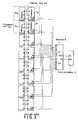
- Fig.1 is a block diagram of the parallel signal process system according to the present invention.
- the feature of Fig.1 as compared with the prior art is the presence of a transparent memory unit 10 inserted between the processor 1 and the memory 2 so that the host processor 4 can access a plurality of processor units 6 at the same time.
- the transparent memory 10 which is the feature of the present invention is now described in detail together with the memory 2.
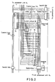
- Fig.2 is a block diagram of the transparent memory according to the present invention.
- the numeral 11 (11a, 11b) is a first bus for connecting the memory 2 to the processor 1 (not shown), 11a is an address bus (data bus), 11b is a control bus, 12 (12a, 12b) is a second bus for connecting the adjacent processor units 6 to one another, 12a is an address bus (data bus), 12b is a control bus, 13 and 14 are first switches having, for example, three states buffers for switching the first bus and the second bus 12 (13a and 14a are switches for address bus (data bus), and 13b and 14b are switches for control bus), 15 is an inverter for inverting the switches 13 and 14 in the first switch, 16 is a bothway switch (second switch) for switching the direction of the first address bus 12a between the direction A and the direction B, 17 is a logical OR circuit for providing the logical sum of the data read out of the memories 2 and the data read out of other processor units (not shown), and 18 is a
- the logical OR circuit 17 is shown by the usual binary positive logical manner in the embodiment, and it should be noted that the OR circuit is replaced by the AND circuit when the circuit is in negative logical manner.
- the third memory 2 and the third transparent memory unit 10 in n number of memories 2 and the units 10 are shown.
- the divided sub-signal is processed by the processor 13, and the result is stored in the memory 23 through the first switches 13a and 13b and the first buses 11a and 11b. That operation is the same as that of the prior art.
- the host processor 4 which intends to read out the results of the process (the host processor 4 at the bottom of Fig.1) accesses all the memories 2a through 2n simultaneously, by connecting the switches 14a and 14b in the first switch group which includes the switches 13a, 13b, 14a and 14b, and by switching the second switch 16 to the direction B.
- the address signal is transferred to the adjacent processor unit through the bothway switch 16.
- the address signal from the host processor 4 is applied to the terminals A0 through A7 of the memory 2 of all the processor units 6a through 6n as the common address simultaneously, and the logical sum of the content in said common addresses of all the memories 2a through 2n at the output terminals D0 through D7 is accomplished by the logic circuit 17 (OR circuit).
- a latch circuit 18 is provided for keeping the data read out of the memories, as the data read out of the memories is lost in a short time.
- the bothway switch 16 is switched from the direction B to the direction A when the data is read out after the address signal is applied to the memories.
- the address to which the process result is stored differs from the address for every processors 1a through 1n, and the null data 0 (all 0 bits word) is stored in the address of the other processors. Therefore, the host processor 4 can take the result which the host processor 4 wishes, although the host processor 4 does not recognize which processor provides that result, in spite of the logic OR operation, since only one input to the OR circuit has information, but the others are null.
- each memories 2a through 2n has not only the bus for the processors 1a through 1n, but also the other bus for the host processor 4 independently, and the host processor 4 can access all the memories simultaneously and directly. Therefore, the present invention is advantageous to process the signal which has the two dimensions, and a signal is divided to small blocks of two dimensions so that each block is processed by the processors 1a through 1n each related to the block.
- the example of that signal which has two dimensions is a picture signal.
- each processor 1a through 1n may be asynchronous from other processors in operation, and therefore, the total parallel process capability is increased considerably.
- each processor 1a through 1n must have a frame memory of one frame, and that frame memory is implemented by a single chip memory which has the capacity of 256 cells x 256 lines x 1 byte.
- the present invention has a processor unit 6 which has a transparent memory between a processor 1 and a memory 2, and therefore, a host processor 4 can access all the memories 2a through 2n simultaneously to read out the memories. Therefore, the high speed parallel process is accomplished, and even when the number of processor units 6 increases, the control of the processor units is simple. Therefore, the present invention is applicable to a picture signal process, and/or other signal process which has large amount of information, and the effect of the invention is large.
- the present invention is used for the high speed parallel signal processing of a signal which has large amount of information, like a picture signal. So, the present invention can be used in such apparatuses, for instance, a television standard conversion apparatus, an information compression apparatus for narrow band transmission of a moving picture signal.
Landscapes
- Engineering & Computer Science (AREA)
- Physics & Mathematics (AREA)
- General Engineering & Computer Science (AREA)
- Theoretical Computer Science (AREA)
- Mathematical Physics (AREA)
- Computer Hardware Design (AREA)
- General Physics & Mathematics (AREA)
- Multi Processors (AREA)
- Image Processing (AREA)
Claims (2)
- System für parallele Signalverarbeitung mit einer Vielzahl von Prozessoreinheiten, die jeweils einen Prozessor zur Verarbeitung eines Signals, das in eine Vielzahl von Teilsignalen unterteilt ist, und einen Speicher aufweisen, der mit dem erwähnten Prozessor über einen internen Bus zur Speicherung der Ergebnisse der durch den erwähnten Prozessor bewirkten Verarbeitung unter einer vorbestimmten Adresse, die dem erwähnten einen Prozessor zugeordnet ist, verbunden ist, wobei das Null-Datum 0 unter der erwähnten vorbestimmten Adresse aller anderen Prozessor-Speicher gespeichert wird, und mit einem Wirtsprozessor zum Steuern der Vielzahl von Prozessoreinheiten, wobei der Wirtsprozessor Signale ausliest, die durch die Vielzahl von Prozessoreinheiten parallel verarbeitet wurden, und wobei das System ferner aufweist:
einen ersten Bus (11a, 11b) zum Verbinden des erwähnten Prozessors mit dem erwähnten Speicher,
einen zweiten Bus (12a, 12b) zum Verbinden benachbarter Prozessoreinheiten mit dem erwähnten Wirtsprozessor,
einen ersten Schalter (13a, 13b, 14a, 14b) zum Umschalten des erwähnten ersten Bus und des erwähnten zweiten Bus,
einen zweiten Schalter (16) zum Umschalten der Richtung des erwähnten zweiten Bus zum Übertragen des Adressensignals in den entsprechenden Speicher oder zum Auslesen der Daten aus dem entsprechenden Speicher, wobei
der erste und der zweite Schalter so geschaltet werden, daß durch eine Vielzahl von Prozessoreinheiten verarbeitete Signale durch den Wirtsprozessor ausgelesen werden. - System zur parallelen Signalverarbeitung nach Anspruch 1, bei dem Ausgänge einer Vielzahl von Speichern (2a...2n) dem Wirtsprozessor (4) über eine ODER-Schaltung zugeführt werden, deren Eingang ein Ausgang jedes Speichers ist.
Applications Claiming Priority (3)
| Application Number | Priority Date | Filing Date | Title |
|---|---|---|---|
| JP78120/88 | 1988-04-01 | ||
| JP63078120A JPH01253059A (ja) | 1988-04-01 | 1988-04-01 | 並列信号処理方式 |
| PCT/JP1989/000351 WO1989009448A1 (fr) | 1988-04-01 | 1989-04-01 | Systeme de traitement de signaux en parallele |
Publications (3)
| Publication Number | Publication Date |
|---|---|
| EP0369022A1 EP0369022A1 (de) | 1990-05-23 |
| EP0369022A4 EP0369022A4 (en) | 1992-05-13 |
| EP0369022B1 true EP0369022B1 (de) | 1995-08-02 |
Family
ID=13653025
Family Applications (1)
| Application Number | Title | Priority Date | Filing Date |
|---|---|---|---|
| EP89904226A Expired - Lifetime EP0369022B1 (de) | 1988-04-01 | 1989-04-01 | System fuer parallele signalverarbeitung |
Country Status (5)
| Country | Link |
|---|---|
| US (1) | US5084836A (de) |
| EP (1) | EP0369022B1 (de) |
| JP (1) | JPH01253059A (de) |
| DE (1) | DE68923684T2 (de) |
| WO (1) | WO1989009448A1 (de) |
Families Citing this family (8)
| Publication number | Priority date | Publication date | Assignee | Title |
|---|---|---|---|---|
| US5055999A (en) | 1987-12-22 | 1991-10-08 | Kendall Square Research Corporation | Multiprocessor digital data processing system |
| IE63461B1 (en) * | 1989-09-11 | 1995-04-19 | Jeremy Owen Jones | Improvements in and relating to stable memory circuits |
| ES2139583T3 (es) * | 1992-08-19 | 2000-02-16 | Siemens Nixdorf Inf Syst | Sistema multiprocesador con memorias cache. |
| ATE195596T1 (de) * | 1994-01-10 | 2000-09-15 | Dow Chemical Co | Ein massiv multiplexierter, superskalarer prozessor mit harvard-architektur |
| US5464435A (en) * | 1994-02-03 | 1995-11-07 | Medtronic, Inc. | Parallel processors in implantable medical device |
| US5555424A (en) * | 1994-10-06 | 1996-09-10 | The Dow Chemical Company | Extended Harvard architecture computer memory system with programmable variable address increment |
| US5949982A (en) * | 1997-06-09 | 1999-09-07 | International Business Machines Corporation | Data processing system and method for implementing a switch protocol in a communication system |
| EP1384160A2 (de) * | 2001-03-02 | 2004-01-28 | Atsana Semiconductor Corp. | Gerät zur berechnung mit variabler wortlänge in einem gatterprozessor |
Family Cites Families (3)
| Publication number | Priority date | Publication date | Assignee | Title |
|---|---|---|---|---|
| US4204251A (en) * | 1977-12-28 | 1980-05-20 | Finn Brudevold | Interconnection unit for multiple data processing systems |
| JPS5899868A (ja) * | 1981-12-08 | 1983-06-14 | Nec Corp | 並列処理方式 |
| JPS59157761A (ja) * | 1983-02-25 | 1984-09-07 | Hitachi Ltd | 線形計画問題計算用並列デ−タ処理方式 |
-
1988
- 1988-04-01 JP JP63078120A patent/JPH01253059A/ja active Pending
-
1989
- 1989-04-01 WO PCT/JP1989/000351 patent/WO1989009448A1/ja not_active Ceased
- 1989-04-01 DE DE68923684T patent/DE68923684T2/de not_active Expired - Fee Related
- 1989-04-01 EP EP89904226A patent/EP0369022B1/de not_active Expired - Lifetime
- 1989-07-26 US US07/399,555 patent/US5084836A/en not_active Expired - Fee Related
Also Published As
| Publication number | Publication date |
|---|---|
| JPH01253059A (ja) | 1989-10-09 |
| WO1989009448A1 (fr) | 1989-10-05 |
| DE68923684D1 (de) | 1995-09-07 |
| DE68923684T2 (de) | 1996-01-25 |
| US5084836A (en) | 1992-01-28 |
| EP0369022A1 (de) | 1990-05-23 |
| EP0369022A4 (en) | 1992-05-13 |
Similar Documents
| Publication | Publication Date | Title |
|---|---|---|
| US4571676A (en) | Memory module selection and reconfiguration apparatus in a data processing system | |
| US4467443A (en) | Bit addressable variable length memory system | |
| US5345573A (en) | High speed burst read address generation with high speed transfer | |
| US4447878A (en) | Apparatus and method for providing byte and word compatible information transfers | |
| US6212597B1 (en) | Apparatus for and method of architecturally enhancing the performance of a multi-port internally cached (AMPIC) DRAM array and like | |
| EP0057511B1 (de) | Informationsverarbeitungseinheit | |
| US4561072A (en) | Memory system handling a plurality of bits as a unit to be processed | |
| US6223260B1 (en) | Multi-bus data processing system in which all data words in high level cache memories have any one of four states and all data words in low level cache memories have any one of three states | |
| CN86107763B (zh) | 具有相邻地址空间的存贮器系统 | |
| EP0369022B1 (de) | System fuer parallele signalverarbeitung | |
| JPH03105789A (ja) | 半導体記憶装置 | |
| US5572695A (en) | Transparent memory mapping mechanism for a digital signal processing system | |
| EP0367995B1 (de) | Vektordatenübertragungssteuerung | |
| US5307321A (en) | Semiconductor memory device with particular bank selector means | |
| US5428801A (en) | Data array conversion control system for controlling conversion of data arrays being transferred between two processing systems | |
| US4644469A (en) | Addressing system for electronic computer | |
| US4618946A (en) | Dual page memory system having storage elements which are selectively swapped between the pages | |
| EP0176976B1 (de) | Plattenspeichersteuergerät mit geteiltem Adressenregister | |
| EP0192209B1 (de) | Adresskonkurrenzarbiter für "multi-port" Speicher | |
| US6442643B1 (en) | System and method for resolving data transfer incompatibilities between PCI and Non-PCI buses | |
| JPH0447920B2 (de) | ||
| JPH0715670B2 (ja) | デ−タ処理装置 | |
| JPS63156291A (ja) | 画像メモリ | |
| CN1013069B (zh) | 多通道控制器 | |
| JPS61260349A (ja) | メモリ選択方式 |
Legal Events
| Date | Code | Title | Description |
|---|---|---|---|
| PUAI | Public reference made under article 153(3) epc to a published international application that has entered the european phase |
Free format text: ORIGINAL CODE: 0009012 |
|
| 17P | Request for examination filed |
Effective date: 19891221 |
|
| AK | Designated contracting states |
Kind code of ref document: A1 Designated state(s): DE GB |
|
| A4 | Supplementary search report drawn up and despatched |
Effective date: 19920324 |
|
| AK | Designated contracting states |
Kind code of ref document: A4 Designated state(s): DE GB |
|
| 17Q | First examination report despatched |
Effective date: 19941012 |
|
| GRAA | (expected) grant |
Free format text: ORIGINAL CODE: 0009210 |
|
| AK | Designated contracting states |
Kind code of ref document: B1 Designated state(s): DE GB |
|
| REF | Corresponds to: |
Ref document number: 68923684 Country of ref document: DE Date of ref document: 19950907 |
|
| PLBE | No opposition filed within time limit |
Free format text: ORIGINAL CODE: 0009261 |
|
| STAA | Information on the status of an ep patent application or granted ep patent |
Free format text: STATUS: NO OPPOSITION FILED WITHIN TIME LIMIT |
|
| 26N | No opposition filed | ||
| PGFP | Annual fee paid to national office [announced via postgrant information from national office to epo] |
Ref country code: GB Payment date: 19980312 Year of fee payment: 10 |
|
| PGFP | Annual fee paid to national office [announced via postgrant information from national office to epo] |
Ref country code: DE Payment date: 19980318 Year of fee payment: 10 |
|
| PG25 | Lapsed in a contracting state [announced via postgrant information from national office to epo] |
Ref country code: GB Free format text: LAPSE BECAUSE OF NON-PAYMENT OF DUE FEES Effective date: 19990401 |
|
| GBPC | Gb: european patent ceased through non-payment of renewal fee |
Effective date: 19990401 |
|
| PG25 | Lapsed in a contracting state [announced via postgrant information from national office to epo] |
Ref country code: DE Free format text: LAPSE BECAUSE OF NON-PAYMENT OF DUE FEES Effective date: 20000201 |