EP0369621B1 - Flüssigkristall-Anzeigevorrichtung - Google Patents
Flüssigkristall-Anzeigevorrichtung Download PDFInfo
- Publication number
- EP0369621B1 EP0369621B1 EP89310955A EP89310955A EP0369621B1 EP 0369621 B1 EP0369621 B1 EP 0369621B1 EP 89310955 A EP89310955 A EP 89310955A EP 89310955 A EP89310955 A EP 89310955A EP 0369621 B1 EP0369621 B1 EP 0369621B1
- Authority
- EP
- European Patent Office
- Prior art keywords
- display electrodes
- liquid crystal
- display
- substrate
- thin film
- Prior art date
- Legal status (The legal status is an assumption and is not a legal conclusion. Google has not performed a legal analysis and makes no representation as to the accuracy of the status listed.)
- Expired - Lifetime
Links
- 239000004973 liquid crystal related substance Substances 0.000 title claims description 66
- 239000000758 substrate Substances 0.000 claims description 58
- 239000010408 film Substances 0.000 claims description 32
- 238000009413 insulation Methods 0.000 claims description 25
- 239000010409 thin film Substances 0.000 claims description 19
- 239000011159 matrix material Substances 0.000 claims description 12
- 230000005540 biological transmission Effects 0.000 claims description 10
- 239000011521 glass Substances 0.000 description 11
- 230000007547 defect Effects 0.000 description 5
- 238000004519 manufacturing process Methods 0.000 description 4
- XAGFODPZIPBFFR-UHFFFAOYSA-N aluminium Chemical compound [Al] XAGFODPZIPBFFR-UHFFFAOYSA-N 0.000 description 3
- 229910052782 aluminium Inorganic materials 0.000 description 3
- 229910021417 amorphous silicon Inorganic materials 0.000 description 3
- 238000000034 method Methods 0.000 description 3
- ZOKXTWBITQBERF-UHFFFAOYSA-N Molybdenum Chemical compound [Mo] ZOKXTWBITQBERF-UHFFFAOYSA-N 0.000 description 2
- XUIMIQQOPSSXEZ-UHFFFAOYSA-N Silicon Chemical compound [Si] XUIMIQQOPSSXEZ-UHFFFAOYSA-N 0.000 description 2
- 229910001362 Ta alloys Inorganic materials 0.000 description 2
- 230000002411 adverse Effects 0.000 description 2
- 229910052750 molybdenum Inorganic materials 0.000 description 2
- 239000011733 molybdenum Substances 0.000 description 2
- JZLMRQMUNCKZTP-UHFFFAOYSA-N molybdenum tantalum Chemical compound [Mo].[Ta] JZLMRQMUNCKZTP-UHFFFAOYSA-N 0.000 description 2
- 229910052710 silicon Inorganic materials 0.000 description 2
- 239000010703 silicon Substances 0.000 description 2
- 229910052715 tantalum Inorganic materials 0.000 description 2
- GUVRBAGPIYLISA-UHFFFAOYSA-N tantalum atom Chemical compound [Ta] GUVRBAGPIYLISA-UHFFFAOYSA-N 0.000 description 2
- 229910052581 Si3N4 Inorganic materials 0.000 description 1
- 230000015556 catabolic process Effects 0.000 description 1
- 238000010276 construction Methods 0.000 description 1
- 230000003247 decreasing effect Effects 0.000 description 1
- 238000006731 degradation reaction Methods 0.000 description 1
- 230000000593 degrading effect Effects 0.000 description 1
- 238000010586 diagram Methods 0.000 description 1
- 239000000428 dust Substances 0.000 description 1
- 230000003071 parasitic effect Effects 0.000 description 1
- 230000002093 peripheral effect Effects 0.000 description 1
- 238000005268 plasma chemical vapour deposition Methods 0.000 description 1
- HQVNEWCFYHHQES-UHFFFAOYSA-N silicon nitride Chemical compound N12[Si]34N5[Si]62N3[Si]51N64 HQVNEWCFYHHQES-UHFFFAOYSA-N 0.000 description 1
Images



Classifications
-
- H—ELECTRICITY
- H10—SEMICONDUCTOR DEVICES; ELECTRIC SOLID-STATE DEVICES NOT OTHERWISE PROVIDED FOR
- H10D—INORGANIC ELECTRIC SEMICONDUCTOR DEVICES
- H10D86/00—Integrated devices formed in or on insulating or conducting substrates, e.g. formed in silicon-on-insulator [SOI] substrates or on stainless steel or glass substrates
-
- G—PHYSICS
- G02—OPTICS
- G02F—OPTICAL DEVICES OR ARRANGEMENTS FOR THE CONTROL OF LIGHT BY MODIFICATION OF THE OPTICAL PROPERTIES OF THE MEDIA OF THE ELEMENTS INVOLVED THEREIN; NON-LINEAR OPTICS; FREQUENCY-CHANGING OF LIGHT; OPTICAL LOGIC ELEMENTS; OPTICAL ANALOGUE/DIGITAL CONVERTERS
- G02F1/00—Devices or arrangements for the control of the intensity, colour, phase, polarisation or direction of light arriving from an independent light source, e.g. switching, gating or modulating; Non-linear optics
- G02F1/01—Devices or arrangements for the control of the intensity, colour, phase, polarisation or direction of light arriving from an independent light source, e.g. switching, gating or modulating; Non-linear optics for the control of the intensity, phase, polarisation or colour
- G02F1/13—Devices or arrangements for the control of the intensity, colour, phase, polarisation or direction of light arriving from an independent light source, e.g. switching, gating or modulating; Non-linear optics for the control of the intensity, phase, polarisation or colour based on liquid crystals, e.g. single liquid crystal display cells
- G02F1/133—Constructional arrangements; Operation of liquid crystal cells; Circuit arrangements
- G02F1/136—Liquid crystal cells structurally associated with a semi-conducting layer or substrate, e.g. cells forming part of an integrated circuit
- G02F1/1362—Active matrix addressed cells
- G02F1/136213—Storage capacitors associated with the pixel electrode
Definitions
- the present invention relates to a liquid crystal display device.
- liquid crystal display device of the above structure light is emitted toward the liquid crystal layer from a light source located behind the array substrate, and the light which has passed through the liquid crystal layer is directed from the surface of the filter substrate to external regions, so as to display information on the liquid crystal display device.
- the amount of light passing through the liquid crystal layer varies in accordance with the condition in which the liquid crystal molecules of the liquid crystal layer facing the transparent display electrode plate are arranged.
- the condition in which the liquid crystal molecules are arranged is controlled by a voltage or a display potential applied between the electrode plate and the transparent conductive film.
- each picture element of the liquid crystal display device is applied with a predetermined display potential by the TFT.
- the regions whose liquid crystal transmission factor are controllable are limited to those regions which face the transparent display electrode plate.
- the regions which do not face the transparent display electrode plate cannot be controlled or modified with respect to the liquid crystal transmission factor (such regions will hereinafter be referred to as unmodulated regions).
- a light-shielding layer is normally formed on those portions of the filter substrate which face the unmodulated regions of the liquid crystal layer, thereby shielding light which may leak from the unmodulated regions.
- the ratio of the area, which can be actually used for showing information, to the entire display area of the display device is determined by the area on which the light-shielding layer is not formed.
- this type of display device employs a light-shielding layer wider than the area of the unmodulated regions, and part of the light-shielding layer overlaps the peripheral portions of the display electrode plate.
- the satisfactory display performance of the display device and the manufacturing yield thereof are incompatible with each other. It is for this reason that a conventional display device cannot employ a display electrode plate having a large area.
- the present invention is contrived in consideration of the above circumstances, and its object is to provide a liquid crystal display device wherein the area of the display electrode can be increased without degrading the manufacturing yield.
- the liquid crystal is driven by the second display electrodes. Therefore, the effective display area of the display device is not adversely affected even if the first display electrodes are reduced in size so as to provide a wide space between the first display electrodes and their neighboring signal and address lines. In addition, the first display electrodes and their neighboring signal and address lines are prevented from short-circuiting to each other, due to the provision of the above-mentioned wide space. Accordingly, the number of probable point defects can be reduced and high manufacturing yield can be expected.
- Figs. 1-3 illustrate a liquid crystal display device according to a first embodiment of the present invention.
- the liquid crystal display device is of an active matrix type comprising a plurality of picture element units 10 arranged in a matrix pattern. These units are driven by picture element circuits, and each of the pixel circuits includes thin film transistor (TFT) 12. Each TFT 12 is connected to both address line X and signal line Y, which extend at right angles to each other.
- TFT thin film transistor
- first transparent display electrode layer 28 is also formed in the region surrounded by address and signal lines X and Y.
- TFT 12 has source electrode 30 which is in contact with silicon layer 26. This source electrode is formed on gate insulation layer 24 and is integral with signal line Y.
- TFT 12 also has drain electrode 32 formed on gate insulation layer 24. This drain electrode connects silicon layer 26 and first display electrode layer 28 together, and is of a laminated structure made up of a first layer formed of molybdenum and a second layer of aluminum.
- the above-mentioned transistor matrix array and first display electrode layer 28 are covered with silicon nitride insulation layer 34 formed by use of the plasma CVD process.
- Second transparent display electrode layer 36 is formed on insulation layer 34 to face first display electrode layer 28.
- First and second electrode layers 28 and 36 are ITO layers having a thickness of 700 ⁇ .
- Second electrode layer 36 is substantially rectangular and has a surface area wider than that of first electrode layer 28.
- Second electrode layer 36 is formed in such a manner that its outline falls within the region defined between first electrode layer 28 and address and signal lines X and Y. Both insulation layer 34 and second electrode layer 36 are covered with orientation layer 38 by which the liquid crystal molecules of liquid crystal layer 18 are orientated.
- Filter substrate 16 has glass plate 40, on one surface of which are formed transparent filter layer 42 facing second display electrode layer 36, and light-shielding layer 44 facing TFT 12, address line X, and signal line Y.
- Transparent conductive layer 46 and orientation layer 48 are formed in the mentioned order on filter layer 42 and also on light-shielding layer 44.
- Liquid crystal layer 18 is sealed between orientation layer 38 of array substrate 14 and orientation layer 48 of filter substrate 16.
- first transparent display electrode layers 28 serve as an electrode for storing charges
- second transparent display electrode layers 36 serve as a display electrode for controlling the orientation of the liquid crystal molecules of liquid crystal layer 18.
- first electrode layer 28 and transparent conductive film 46 of filter substrate 16 part of the potential stored between layer 28 and film 46, i.e., the partial voltage corresponding to the electric capacity at the location of second electrode layer 36, is applied to second electrode layer 36.
- the transmission factor of that region of liquid crystal layer 18 which faces second electrode layer 36 is modulated.
- the electric capacity obtained from first and second electrode layers 28 and 36 is larger than the electric capacity obtained from second electrode layer 36 and transparent conductive film 46, so as to improve the driving efficiency of the liquid crystal layer.
- the thickness of insulation layer 34 is determined to be 5,000 ⁇
- the thickness of the liquid crystal layer is determined to be 60,000 ⁇
- the capacity ratio between insulation layer 34 and the liquid crystal layer is determined to be about 10:1.
- each second display electrode layer 36 which serves as a virtual display electrode, is located sufficiently away from the electrodes of thin film transistor 12, the address line, and the signal line.
- second display electrode layer 36 is formed on insulation layer 34, it is insulated from the electrodes of thin film transistor 12, the address line, and the signal line.
- each second display electrode layer 36 can have a sufficiently wide surface area, without causing the problem that second display electrode layer 36 may be short-circuited to the electrodes of transistor 12, or to the address and signal lines. Therefore, the aperture ratio of the display device can be increased. Further, the size of the surface area of first display electrode layer 28 does not adversely affect the aperture ratio of the display device.
- first display electrode layer 28 can be decreased, so as to provide a sufficiently wide space between layer 28 and its neighboring elements namely, the electrodes of transistor 12, the address line, and the signal line. This structure is effective in reliably preventing occurrence of short circuit between the electrodes.
- Figs. 4 and 5 illustrate a liquid crystal display device according to a second embodiment of the present invention. Since the basic structure of the device of the second embodiment is substantially similar to that of the first embodiment, similar or corresponding structural elements will be indicated by the same reference numerals, and explanation of them will be omitted.
- each address line X is of a laminated structure made up of a 1,000 ⁇ - thick molybdenum-tantalum alloy film as a first layer and a 1,500 ⁇ - thick tantalum film as a second layer.
- Each signal line Y is also of a laminated structure made up of a 500 ⁇ - thick molybdenum film as a first layer and a 4,000 ⁇ - thick aluminum film as a second layer.
- Each second transparent display electrode layer 36 is formed, in a self-alignment fashion, within the region surrounded by address lines X and signal lines Y. In other words, second display electrode layer 36 is has the same shape and same size as the above-mentioned surrounded region.
- the device of the second embodiment produces substantially similar advantages to those of the first embodiment.
- light A emitted from behind array substrate 14 passes through every portion of the liquid crystal layer that can be modified by second transparent electrode layers 36. Therefore, the maximum possible aperture ratio is available in the case of the second embodiment.
- filter substrate 16 of the second embodiment does not have to comprise a light-shielding film.
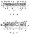
- Second transparent display electrode layer 36 employed in the second embodiment is fabricated as follows: As is shown in Fig. 6, a 700 ⁇ - thick film of transparent electrode 50 (ITO) is first formed on insulation layer 34 which covers first transparent display electrode layer 28s, and then negative type resist layer 52 is coated on electrode 50. Thereafter, array substrate 14 is irradiated with ultraviolet light B emitted from behind glass substrate 20. After passing through glass substrate 20, ultraviolet light B is shielded in part by thin film transistors 12, address lines X and signal lines Y; the remainder of ultraviolet light B passes through first display electrode layers 28, insulation layer 34, and transparent electrode 50, so that resist layer 52 is selectively exposed to ultraviolet light B.
- ITO transparent electrode 50
- resist layer 52 has non-irradiated portion 52a, which has a pattern corresponding to the shapes of thin film transistors 12, address lines X, and signal lines Y, and irradiated portions 52b.
- resist layer 52 is developed and selectively etched out, thereby forming transparent display electrode layers 36 self-aligned with the region surrounded by lines X and Y, as is shown in Fig. 7.
- the self-aligned layers or pattern need not be always formed in the above-mentioned fashion. They may be formed in a lift-off method, using a positive type resist layer and a transparent electrode.
- the first and second embodiments were described, referring to a transmission type liquid crystal display device wherein an image is displayed by use of light emitted from a light source.
- the present invention is not limited to this type of display device. It can be applied to a reflection type liquid crystal display device, as is seen from a third embodiment shown in Figs. 8 and 9.
- each of first display electrodes 28 of array substrate 14 is formed of Cr to to be integral with drain electrode 32 of TFT 12.
- second reflection type display electrode layers 36 formed of aluminum and having a thickness of 2,000 ⁇ are provided, in place of the transparent display electrode layers employed in the foregoing embodiments.
- Each display electrode layer 36 is formed to cover the substantially entire region surrounded by address lines X and signal lines Y, the region located above TFT 12, and part of lines X and Y. It is preferable that second display electrode 36 be formed in a manner to minimize the parasitic capacity between itself and address lines X.
- Transparent conductive film 46 and orientation film 48 are formed on glass substrate 40 of substrate 16 in the order mentioned.
- the liquid crystal display device of the third embodiment is designed such that it can be used also as a projection type display device.
- the rays of incident light C should be substantially parallel to one another; likewise, the rays of reflected light D should be substantially parallel to one another. Therefore, the surfaces of second reflection type display electrode layers 36 should preferably be as specular as possible.
- each display electrode layer 36 can be expanded up to the region located above lines X and Y and up to the region located above TFT 12, so that the display region of the device can be further widened.
- incident light C does not directly enter TFT 12.
- the OFF-state current which may flow through TFT 12 due to external light is prevented from increasing.
- insulation layer 34 separates second display electrode layers 36 from first display electrode layers 28.
- line defects are hard to occur even if signal line Y is short-circuited to first electrode layer 28 and if second display electrode 36 is short-circuited to transparent conductive film 46, etc.
- a sufficiently wide space can be provided between first display electrode layer 28 and signal lines Y, to prevent occurrence of point defects, and second display electrode 36 can be expanded for higher display performance.
Landscapes
- Physics & Mathematics (AREA)
- Engineering & Computer Science (AREA)
- Nonlinear Science (AREA)
- Power Engineering (AREA)
- Microelectronics & Electronic Packaging (AREA)
- Mathematical Physics (AREA)
- Chemical & Material Sciences (AREA)
- Crystallography & Structural Chemistry (AREA)
- General Physics & Mathematics (AREA)
- Optics & Photonics (AREA)
- Liquid Crystal (AREA)
- Devices For Indicating Variable Information By Combining Individual Elements (AREA)
Claims (11)
- Flüssigkristall-Anzeigevorrichtung, bestehend aus:
einem Matrixanordnungssubstrat (14) mit: einem ersten Substrat (20); einer Vielzahl von Dünnfilmtransistoren (12), die auf dem Substrat angeordnet sind; Signalleitungen (Y) und Adreßleitungen (X), die mit den Dünnfilmtransistoren verbunden sind; und einer Vielzahl von ersten Anzeigeelektroden (28), die auf dem Substrat angeordnet und mit entsprechenden der Dünnfilmtransistoren verbunden sind, um Ladungen zu speichern, die von den Dünnfilmtransistoren angelegt sind;
einem oberen Substrat (16) mit einem zweiten Substrat (40), das mit einem transparenten leitenden Film (46) versehen ist, der den ersten Anzeigeelektroden gegenüberliegt; und
einer Flüssigkristallschicht (18), die zwischen dem Matrixanordnungssubstrat und dem oberen Substrat angeordnet ist, wobei die Flüssigkristallschicht einen Transmissions- bzw. Durchlässigkeitsfaktor hat, der in Übereinstimmung mit einer vorbestimmten treibenden Spannung, die darüber angelegt ist, variiert bzw. verschieden ist;
dadurch gekennzeichnet, daß:
das Matrixanordnungssubstrat (14) einen Isolierfilm (34), der die Dünnfilmtransistoren (12), die Signalleitungen (Y), die Adreßleitungen (X) und die ersten Anzeigeelektroden (28) bedeckt; und eine Vielzahl von zweiten Anzeigeelektroden (36) beinhaltet, die auf dem Isolierfilm angeordnet sind und entsprechenden der ersten Anzeigeelektroden gegenüberliegen, um eine Kapazitätsverbindung mit den ersten Anzeigeelektroden zu bilden, so daß die zweiten Anzeigeelektroden von den ersten Anzeigeelektroden mit einer Spannung versorgt sind, wenn eine vorbestimmte Spannung an die ersten Anzeigeelektroden angelegt ist; und
der Transmissionsfaktor der Flüssigkristallschicht (18) in Übereinstimmung mit der vorbestimmten treibenden Spannung, die zwischen den zweiten Anzeigeelektroden und dem transparenten, leitenden Film (46) angelegt ist, verschieden ist. - Vorrichtung nach Anspruch 1, dadurch gekennzeichnet, daß jede der zweiten Anzeigeelektroden (36) eine Oberflächenfläche hat, die weiter ist als die der entsprechenden ersten Anzeigeelektrode (28) und gebildet ist, um die entsprechende erste Anzeigeelektrode zu bedecken.
- Vorrichtung nach Anspruch 1, dadurch gekennzeichnet, daß die Adreßleitungen (X) und die Signalleitungen (Y) einander kreuzen und jede der ersten Anzeigeelektroden (28) und die entsprechende zweite Anzeigeelektrode (36) sich in einer Region befinden, die von den Adreß- und Signalleitungen umgeben ist.
- Vorrichtung nach Anspruch 3, dadurch gekennzeichnet, daß jede der zweiten Anzeigeelektroden (38) eine Form und eine Größe hat, die denen der Region, die von den Adreß- und Signalleitungen (X, Y) umgeben ist, wesentlich ähnlich sind.
- Vorrichtung nach Anspruch 3, dadurch gekennzeichnet, daß die ersten und zweiten Elektroden (28, 36) transparent sind.
- Vorrichtung nach Anspruch 5, dadurch gekennzeichnet, daß das obere Substrat (16) lichtabschirmende Filme (44) beinhaltet, die positioniert sind, um den Adreßleitungen (X), den Signalleitungen (Y) und den Dünnfilmtransistoren (12) gegenüberzuliegen.
- Vorrichtung nach Anspruch 1, dadurch gekennzeichnet, daß jede der zweiten Anzeigeelektroden (36) eine Reflexionstypelektrode ist, die durch die Flüssigkristallschicht (18) darauf einfallendes Licht auf eine externe Region der Vorrichtung durch die Flüssigkristallschicht reflektiert.
- Vorrichtung nach Anspruch 7, dadurch gekennzeichnet, daß jede der zweiten Anzeigeelektroden (36) eine Oberflächenfläche hat, die weiter ist als die der entsprechenden ersten Anzeigeelektrode (28) und gebildet ist, um die entsprechende erste Anzeigeelektrode zu bedecken.
- Vorrichtung nach Anspruch 8, dadurch gekennzeichnet, daß die Adreßleitungen (X) und die Signalleitungen (Y) einander kreuzen und jede der ersten Anzeigeelektroden (28) sich in einer Region befindet, die von den Adreß- und Signalleitungen umgeben ist.
- Vorrichtung nach Anspruch 9, dadurch gekennzeichnet, daßjede der zweiten Anzeigeelektroden (36) gebildet ist, um die umgebene Region im wesentlichen vollständig und den entsprechenden Dünnfilmtransistor (12) zu bedecken.
- Flüssigkristall-Anzeigevorrichtung, bestehend aus:
einem Matrixanordnungssubstrat (14) mit: einem ersten Substrat (20); einer Vielzahl von Dünnfilmtransistoren (12), die auf dem Substrat angeordnet sind; Signalleitungen (Y) und Adreßleitungen (X), die mit den Dünnfilmtransistoren verbunden sind; und einer Vielzahl von ersten transparenten Anzeigeelektroden (28), die auf dem Substrat angeordnet und mit entsprechenden der Dünnfilmtransistoren verbunden sind, um Ladungen zu speichern, die von den Dünnfilmtransistoren angelegt sind;
einem oberen Substrat (16) mit einem zweiten Substrat (40), das mit einem transparenten leitenden Film (46) versehen ist, der den ersten Anzeigeelektroden gegenüberliegt; und
einer Flüssigkristallschicht (18), die zwischen dem Matrixanordnungssubstrat und dem oberen Substrat angeordnet ist, wobei die Flüssigkristallschicht einen Transmissionsfaktor hat, der in Übereinstimmung mit einer vorbestimmten treibenden Spannung, die darüber angelegt ist, variiert bzw. verschieden ist;
dadurch gekennzeichnet, daß:
das Matrixanordnungssubstrat (14) einen Isolierfilm (34), der die Dünnfilmtransistoren (12), die Signalleitungen (Y), die Adreßleitungen (X) und die ersten Anzeigeelektroden (28) bedeckt; und eine Vielzahl von zweiten transparenten Anzeigeelektroden (36) beinhaltet, die auf dem Isolierfilm angeordnet sind und entsprechenden der ersten Anzeigeelektroden gegenüberliegen, um eine Kapazitätsverbindung mit den ersten Anzeigeelektroden zu bilden, so daß die zweiten Anzeigeelektroden von den ersten Anzeigeelektroden mit einer Spannung versorgt sind, wenn eine vorbestimmte Spannung an die ersten Anzeigeelektroden angelegt ist; und
der Transmissionsfaktor der Flüssigkristallschicht (18) in Übereinstimmung mit der vorbestimmten treibenden Spannung, die zwischen den zweiten Anzeigeelektroden und dem transparenten, leitenden Film (46) angelegt ist, verschieden ist.
Applications Claiming Priority (2)
| Application Number | Priority Date | Filing Date | Title |
|---|---|---|---|
| JP28677188 | 1988-11-15 | ||
| JP286771/88 | 1988-11-15 |
Publications (3)
| Publication Number | Publication Date |
|---|---|
| EP0369621A2 EP0369621A2 (de) | 1990-05-23 |
| EP0369621A3 EP0369621A3 (de) | 1991-04-10 |
| EP0369621B1 true EP0369621B1 (de) | 1994-06-08 |
Family
ID=17708837
Family Applications (1)
| Application Number | Title | Priority Date | Filing Date |
|---|---|---|---|
| EP89310955A Expired - Lifetime EP0369621B1 (de) | 1988-11-15 | 1989-10-24 | Flüssigkristall-Anzeigevorrichtung |
Country Status (3)
| Country | Link |
|---|---|
| US (1) | US5042918A (de) |
| EP (1) | EP0369621B1 (de) |
| DE (1) | DE68915947T2 (de) |
Families Citing this family (40)
| Publication number | Priority date | Publication date | Assignee | Title |
|---|---|---|---|---|
| US5058995A (en) * | 1990-03-15 | 1991-10-22 | Thomson Consumer Electronics, Inc. | Pixel electrode structure for liquid crystal display devices |
| JPH06208132A (ja) * | 1990-03-24 | 1994-07-26 | Sony Corp | 液晶表示装置 |
| JP2622183B2 (ja) * | 1990-04-05 | 1997-06-18 | シャープ株式会社 | アクティブマトリクス表示装置 |
| JPH0431826A (ja) * | 1990-05-29 | 1992-02-04 | Alps Electric Co Ltd | 液晶表示素子 |
| US5245450A (en) * | 1990-07-23 | 1993-09-14 | Hosiden Corporation | Liquid crystal display device with control capacitors for gray-scale |
| JP2650780B2 (ja) * | 1990-11-30 | 1997-09-03 | シャープ株式会社 | アクティブマトリクス基板 |
| US5206749A (en) * | 1990-12-31 | 1993-04-27 | Kopin Corporation | Liquid crystal display having essentially single crystal transistors pixels and driving circuits |
| US5302987A (en) * | 1991-05-15 | 1994-04-12 | Sharp Kabushiki Kaisha | Active matrix substrate including connecting electrode with extended portion |
| JP2753160B2 (ja) * | 1991-10-08 | 1998-05-18 | 株式会社フロンテック | アクティブマトリックス形液晶表示素子の基板 |
| US5576858A (en) * | 1991-10-14 | 1996-11-19 | Hosiden Corporation | Gray scale LCD control capacitors formed between a control capacitor electrode on one side of an insulating layer and two subpixel electrodes on the other side |
| JPH05107556A (ja) * | 1991-10-14 | 1993-04-30 | Hosiden Corp | 液晶表示素子画素 |
| US6693681B1 (en) | 1992-04-28 | 2004-02-17 | Semiconductor Energy Laboratory Co., Ltd. | Electro-optical device and method of driving the same |
| JP2814161B2 (ja) * | 1992-04-28 | 1998-10-22 | 株式会社半導体エネルギー研究所 | アクティブマトリクス表示装置およびその駆動方法 |
| US5707746A (en) * | 1992-09-25 | 1998-01-13 | Sharp Kabushiki Kaisha | Thin film transistor device with advanced characteristics by improved matching between a glass substrate and a silicon nitride layer |
| JP2860226B2 (ja) * | 1993-06-07 | 1999-02-24 | シャープ株式会社 | 液晶表示装置およびその製造方法 |
| JP2975844B2 (ja) * | 1993-06-24 | 1999-11-10 | 三洋電機株式会社 | 液晶表示装置 |
| US7310072B2 (en) | 1993-10-22 | 2007-12-18 | Kopin Corporation | Portable communication display device |
| KR100343376B1 (ko) * | 1993-12-31 | 2002-11-23 | 고려화학 주식회사 | 반도체소자봉지용경화제의제조방법및이를함유하는반도체소자봉지용수지조성물 |
| DE19500380C2 (de) * | 1994-05-20 | 2001-05-17 | Mitsubishi Electric Corp | Aktivmatrix-Flüssigkristallanzeige und Herstellungsverfahren dafür |
| JPH08201853A (ja) * | 1994-11-24 | 1996-08-09 | Toshiba Electron Eng Corp | 電極基板および平面表示装置 |
| KR0171092B1 (ko) * | 1995-07-06 | 1999-05-01 | 구자홍 | 기판 제조방법 |
| JPH09236826A (ja) * | 1995-09-28 | 1997-09-09 | Sharp Corp | 液晶表示素子およびその製造方法 |
| US6197209B1 (en) | 1995-10-27 | 2001-03-06 | Lg. Philips Lcd Co., Ltd. | Method of fabricating a substrate |
| TW335503B (en) * | 1996-02-23 | 1998-07-01 | Semiconductor Energy Lab Kk | Semiconductor thin film and manufacturing method and semiconductor device and its manufacturing method |
| JP3149793B2 (ja) * | 1996-07-22 | 2001-03-26 | 日本電気株式会社 | 反射型液晶表示装置及びその製造方法 |
| US6677936B2 (en) | 1996-10-31 | 2004-01-13 | Kopin Corporation | Color display system for a camera |
| US7372447B1 (en) | 1996-10-31 | 2008-05-13 | Kopin Corporation | Microdisplay for portable communication systems |
| US6486862B1 (en) | 1996-10-31 | 2002-11-26 | Kopin Corporation | Card reader display system |
| US7321354B1 (en) | 1996-10-31 | 2008-01-22 | Kopin Corporation | Microdisplay for portable communication systems |
| JP3269787B2 (ja) * | 1997-05-27 | 2002-04-02 | シャープ株式会社 | 液晶表示装置 |
| US6909419B2 (en) * | 1997-10-31 | 2005-06-21 | Kopin Corporation | Portable microdisplay system |
| US6552704B2 (en) | 1997-10-31 | 2003-04-22 | Kopin Corporation | Color display with thin gap liquid crystal |
| US6476784B2 (en) | 1997-10-31 | 2002-11-05 | Kopin Corporation | Portable display system with memory card reader |
| KR100357213B1 (ko) * | 1998-07-23 | 2002-10-18 | 엘지.필립스 엘시디 주식회사 | 멀티도메인 액정표시소자 |
| CN1244890C (zh) * | 1998-11-26 | 2006-03-08 | 精工爱普生株式会社 | 电光装置及其制造方法和电子装置 |
| US6469317B1 (en) | 1998-12-18 | 2002-10-22 | Semiconductor Energy Laboratory Co., Ltd. | Semiconductor device and method of fabricating the same |
| JP3492582B2 (ja) * | 2000-03-03 | 2004-02-03 | Nec液晶テクノロジー株式会社 | 液晶表示装置及びその製造方法 |
| TWI225177B (en) * | 2001-09-12 | 2004-12-11 | Hannstar Display Corp | Manufacturing method of thin film transistor (TFT) liquid crystal display (LCD) |
| US7359105B2 (en) * | 2006-02-07 | 2008-04-15 | Sharp Kabushiki Kaisha | Spatial light modulator and a display device |
| US8294840B2 (en) * | 2008-03-19 | 2012-10-23 | Chimei Innolux Corporation | Liquid crystal display device with fringe field switching mode |
Family Cites Families (15)
| Publication number | Priority date | Publication date | Assignee | Title |
|---|---|---|---|---|
| US3862360A (en) * | 1973-04-18 | 1975-01-21 | Hughes Aircraft Co | Liquid crystal display system with integrated signal storage circuitry |
| US4103297A (en) * | 1976-12-20 | 1978-07-25 | Hughes Aircraft Company | Light-insensitive matrix addressed liquid crystal display system |
| JPS5764776A (en) * | 1980-10-09 | 1982-04-20 | Nippon Denshi Kogyo Shinko | Liquid crystal display unit |
| EP0071244B1 (de) * | 1981-07-27 | 1988-11-23 | Kabushiki Kaisha Toshiba | Dünnschichttransistor und Verfahren zu dessen Herstellung |
| JPS58205181A (ja) * | 1982-05-26 | 1983-11-30 | セイコーインスツルメンツ株式会社 | マトリクス液晶表示装置 |
| JPS59119390A (ja) * | 1982-12-25 | 1984-07-10 | 株式会社東芝 | 薄膜トランジスタ回路 |
| JPS59119329A (ja) * | 1982-12-27 | 1984-07-10 | Toshiba Corp | 液晶表示装置 |
| JPS6045219A (ja) * | 1983-08-23 | 1985-03-11 | Toshiba Corp | アクテイブマトリクス型表示装置 |
| US4715685A (en) * | 1985-03-04 | 1987-12-29 | Energy Conversion Devices, Inc. | Liquid crystal display having potential source in a diode ring |
| JPS62100734A (ja) * | 1985-10-28 | 1987-05-11 | Seiko Epson Corp | 液晶表示装置 |
| JP2520592B2 (ja) * | 1985-11-08 | 1996-07-31 | キヤノン株式会社 | 液晶表示素子 |
| DE3684150D1 (de) * | 1986-09-26 | 1992-04-09 | Ibm | Halbleiter-integrierte anzeige. |
| JPH0691252B2 (ja) * | 1986-11-27 | 1994-11-14 | 日本電気株式会社 | 薄膜トランジスタアレイ |
| JPS63175832A (ja) * | 1987-01-16 | 1988-07-20 | Hosiden Electronics Co Ltd | アクテイブマトリクス液晶表示装置 |
| US4839707A (en) * | 1987-08-27 | 1989-06-13 | Hughes Aircraft Company | LCMOS displays fabricated with implant treated silicon wafers |
-
1989
- 1989-10-18 US US07/423,206 patent/US5042918A/en not_active Expired - Lifetime
- 1989-10-24 DE DE68915947T patent/DE68915947T2/de not_active Expired - Fee Related
- 1989-10-24 EP EP89310955A patent/EP0369621B1/de not_active Expired - Lifetime
Also Published As
| Publication number | Publication date |
|---|---|
| EP0369621A3 (de) | 1991-04-10 |
| DE68915947D1 (de) | 1994-07-14 |
| US5042918A (en) | 1991-08-27 |
| EP0369621A2 (de) | 1990-05-23 |
| DE68915947T2 (de) | 1994-09-22 |
Similar Documents
| Publication | Publication Date | Title |
|---|---|---|
| EP0369621B1 (de) | Flüssigkristall-Anzeigevorrichtung | |
| US7289188B2 (en) | Defect correction of pixel electrode by connection to gate line | |
| JP2613015B2 (ja) | 液晶表示装置 | |
| KR0145280B1 (ko) | 액티브매트릭스 액정표시장치 | |
| KR100333156B1 (ko) | 표시장치 | |
| USRE38292E1 (en) | Method to prevent static destruction of an active element comprised in a liquid crystal display device | |
| KR100493869B1 (ko) | 횡전계 방식의 액정표시장치 및 그 제조방법 | |
| US6208390B1 (en) | Electrode substrate resistant to wire breakage for an active matrix display device | |
| JPH1010548A (ja) | アクティブマトリクス基板およびその製造方法 | |
| JPS6045219A (ja) | アクテイブマトリクス型表示装置 | |
| US6326641B1 (en) | Liquid crystal display device having a high aperture ratio | |
| KR100838185B1 (ko) | 어레이 기판 및 이를 이용한 액정 표시 장치와, 이의 제조방법 | |
| JP2002091342A (ja) | マトリクスアレイ基板 | |
| US7936424B2 (en) | Liquid crystal display panel with light leakage prevention film and method for manufacturing the same | |
| US20060289867A1 (en) | Liquid crystal display device capable of reducing leakage current, and fabrication method thereof | |
| KR20040055688A (ko) | 전기 광학 기판의 제조 방법, 전기 광학 장치의 제조방법, 전기 광학 장치 | |
| JP2859896B2 (ja) | 液晶表示装置 | |
| JP2000122089A (ja) | 液晶表示装置 | |
| JP2910656B2 (ja) | アクティブマトリクス液晶表示パネル及びその製造方法 | |
| JPH0372324A (ja) | アクティブマトリクス表示装置 | |
| JP3405690B2 (ja) | プラズマアドレス表示装置 | |
| JP2000155323A (ja) | 液晶表示装置 | |
| JPH04195024A (ja) | 液晶表示装置 | |
| JP2025171658A (ja) | 耐湿性の低下を抑制しつつ開口率を向上できるアレイ基板、及び表示装置 | |
| JPH08320503A (ja) | アクティブマトリクス液晶表示パネル |
Legal Events
| Date | Code | Title | Description |
|---|---|---|---|
| PUAI | Public reference made under article 153(3) epc to a published international application that has entered the european phase |
Free format text: ORIGINAL CODE: 0009012 |
|
| 17P | Request for examination filed |
Effective date: 19891114 |
|
| AK | Designated contracting states |
Kind code of ref document: A2 Designated state(s): DE FR GB |
|
| PUAL | Search report despatched |
Free format text: ORIGINAL CODE: 0009013 |
|
| AK | Designated contracting states |
Kind code of ref document: A3 Designated state(s): DE FR GB |
|
| 17Q | First examination report despatched |
Effective date: 19930802 |
|
| GRAA | (expected) grant |
Free format text: ORIGINAL CODE: 0009210 |
|
| AK | Designated contracting states |
Kind code of ref document: B1 Designated state(s): DE FR GB |
|
| PG25 | Lapsed in a contracting state [announced via postgrant information from national office to epo] |
Ref country code: FR Effective date: 19940608 |
|
| REF | Corresponds to: |
Ref document number: 68915947 Country of ref document: DE Date of ref document: 19940714 |
|
| PG25 | Lapsed in a contracting state [announced via postgrant information from national office to epo] |
Ref country code: GB Effective date: 19941024 |
|
| EN | Fr: translation not filed | ||
| PLBE | No opposition filed within time limit |
Free format text: ORIGINAL CODE: 0009261 |
|
| STAA | Information on the status of an ep patent application or granted ep patent |
Free format text: STATUS: NO OPPOSITION FILED WITHIN TIME LIMIT |
|
| 26N | No opposition filed | ||
| GBPC | Gb: european patent ceased through non-payment of renewal fee |
Effective date: 19941024 |
|
| PGFP | Annual fee paid to national office [announced via postgrant information from national office to epo] |
Ref country code: DE Payment date: 20051020 Year of fee payment: 17 |
|
| PG25 | Lapsed in a contracting state [announced via postgrant information from national office to epo] |
Ref country code: DE Free format text: LAPSE BECAUSE OF NON-PAYMENT OF DUE FEES Effective date: 20070501 |