EP0370460A2 - Dispositif de mémoire semi-conducteur - Google Patents
Dispositif de mémoire semi-conducteur Download PDFInfo
- Publication number
- EP0370460A2 EP0370460A2 EP89121518A EP89121518A EP0370460A2 EP 0370460 A2 EP0370460 A2 EP 0370460A2 EP 89121518 A EP89121518 A EP 89121518A EP 89121518 A EP89121518 A EP 89121518A EP 0370460 A2 EP0370460 A2 EP 0370460A2
- Authority
- EP
- European Patent Office
- Prior art keywords
- signal
- column
- row
- section
- operative
- Prior art date
- Legal status (The legal status is an assumption and is not a legal conclusion. Google has not performed a legal analysis and makes no representation as to the accuracy of the status listed.)
- Withdrawn
Links
Images








Classifications
-
- G—PHYSICS
- G11—INFORMATION STORAGE
- G11C—STATIC STORES
- G11C11/00—Digital stores characterised by the use of particular electric or magnetic storage elements; Storage elements therefor
- G11C11/21—Digital stores characterised by the use of particular electric or magnetic storage elements; Storage elements therefor using electric elements
- G11C11/34—Digital stores characterised by the use of particular electric or magnetic storage elements; Storage elements therefor using electric elements using semiconductor devices
-
- G—PHYSICS
- G11—INFORMATION STORAGE
- G11C—STATIC STORES
- G11C8/00—Arrangements for selecting an address in a digital store
- G11C8/10—Decoders
Definitions
- This invention relates to a semiconductor memory device, and more particularly to a synchronous semiconductor memory device such as a RAM or a ROM.
- a synchronous memory as the background art and its timing chart are shown in FIGS. 22 and 23, respectively.
- a row address is applied to a latch 12 and is latched in synchronism with a synchronizing signal ⁇ . After the latch time t lat , this signal is applied to a row decoder 11. After an address decode time t dec , the row decoder 11 applies a row decoded signal to a memory cell array 14 through one of the corresponding word lines 13, 13, ⁇ .
- a column address is applied to a latch 17, and is latched in synchronism with the synchronizing signal ⁇ . After the latch time t lat , this signal is applied to a column decoder 16.
- the column decoder 16 After the address decode time t dec , the column decoder 16 applies a column decoded signal to an input/output circuit 19 to select one of corresponding bit lines 18, 18, ⁇ .
- the row decoded signal is thus outputted to the corresponding word line 13, and the corresponding bit line 18 is selected in accordance with the column decoded signal, data from the memory cell array 14 is read out to the data line 20 after a sense time t sense , with the data setup time t ds being ensured.
- the above-mentioned cycles are repeatedly executed.
- the readout of data corresponding to the respective addresses is sequentially executed.
- This invention has been made in view of the above, and its object is to provide a semiconductor memory device having a short cycle time.
- a row address is first decoded at the row decoder.
- the signal thus decoded is latched at a latch circuit.
- the word line is driven by an output from the latch circuit.
- a section address is first decoded at the section decoder, and the signal thus decoded is latched at the latch circuit.
- a section select line is driven by an output from the latch circuit. Data read or write operation through an input/output circuit is applied to the specified cell defined by driving the corresponding word and section select lines.
- a new row address is transmitted to the row decoder as it is through the master latch circuit at the latter half of one cycle of the synchronizing signal.
- the row decoder initiates the decoding operation.
- the synchronizing signal shifts to the next cycle.
- the master latch circuit latches an input being inputted at that time (new row address).
- the decoding operation of the row address is completed.
- the decoded signal drives the word line through the slave-latch circuit.
- the section decoder initiates the decoding operation.
- the synchronizing signal shifts to the next cycle.
- the master latch circuit latches an input being inputted at that time (new section address).
- the decoding operation of the section address is completed.
- the decoded signal drives a section select line through the slave latch circuit. By driving the corresponding word and section select lines, double word line structure (driving) is implemented. Data read is conducted from a certain cell through the input/output circuit and data write is conducted into the cell therethrough.
- the entire address decode time is not included in one cycle time, but a portion of the address decode time, i.e., only a time period from the time when the cycle of the synchronizing signal changes to the time when the address decoding is completed is included in one cycle time.
- the cycle time is shortened.
- row address decoding and data sensing are subjected to pipe-line processing.
- the cycle time in the semiconductor memory device can be shortened.
- the cycle time can be shortened also in a large capacity memory of the double word line structure.
- FIG. 1 there is shown a first embodiment of this invention.
- This embodiment differs from the background art in that after row and column addresses are decoded, they are latched and are then applied to the memory cell array.
- the row address is applied to the memory cell array 14 through the row decoder 11, the latch 12, and a corresponding word line 13.
- the column address serves to select a corresponding bit line 18 through the column decoder 16, the latch 17, the input/output circuit 19.
- the row address is applied to the row decoder 11, and is then applied to the latch 12 as a row decoded signal.
- the latch 12 takes into a row decoded signal in synchronism with a synchronizing signal (clock) ⁇ to drive a corresponding one of word lines 13, 13, ⁇ .
- the column address is applied to the column decoder 16, and is then applied to the latch 17 as a column decoded signal.
- the latch 17 takes into the column decoded signal in synchronism with the synchronizing signal ⁇ to select, as a column select signal, a corresponding bit line 18 through the input/output circuit 19.
- FIG. 2 there is shown a timing chart showing the operation of the latches 12 and 17.
- These latches 12 and 17 take an input IN (A) thereinto in response to the rise of the synchronizing signal ⁇ to output an output OUT (A). This output (A) is maintained during one cycle of the synchronizing signal.
- These latches 12 and 17 take an input IN (B) thereinto in response to the next rise of the synchronizing signal ⁇ to output the output (B) in place of the output OUT (A) until now.
- FIG. 3 there is shown a timing chart showing the read operation of the memory.
- row and column decoded signals are defined at time t1 when the address decode time t dec has passed.
- the row and column decoded signals previously defined are taken into the latches 12 and 17, respectively.
- the word line 13 is driven and a corresponding bit line 18 is selected by the column select signal.
- time t4 when the data sense time t sense has passed from the time t3, data is outputted to the data line 20.
- time t5 when the data setup time t ds has passed from the time t4, execution of one cycle is completed.
- the equation (2) does not include the address decode time t dec which is included in the equation (1). Namely, it is seen that the cycle time t′ cycle is shorter than the cycle time t cycle by the time t dec .
- the address decode time t dec occupies about 50% of the access time (cycle time t cycle ).
- the cycle time t′ cycle expressed as the equation (2) can be set to a value of about one half of the cycle time t cycle expressed as the equation (1).
- a dynamic latch circuit or a static latch circuit may be used.
- the dynamic latch circuit e.g, circuits as shown in FIGS. 4 and 5 may be used.
- C-CMOS clocked CMOS
- This circuit is constructed as a dynamic circuit of a structure consisting of two C-CMOSs.
- a transfer gate TG structure of the CMOS type is used as the switch circuit.
- This circuit is constructed as a dynamic circuit of a structure consisting of two transfer gates TG and two inverters IV.
- static latch circuit e.g., circuits as shown in FIGS. 6 and 7 may be used.
- the circuit shown in FIG. 6 is constructed as a static latch circuit of a structure such that loop circuits each consisting of an inverter IV and a C-CMOS are connected to the respective output sides of the two C-CMOSs of the latch circuit shown in FIG. 4.
- the circuit shown in FIG. 7 is constructed as a static latch circuit of a structure in which feedback is applied to respective two inverters of the latch circuit shown in FIG. 5 by the series circuit including an inverter IV and a transfer gate TG.
- latches 12, 17 shown in FIG. 1 are not limited to the latch circuit shown in FIGS. 4 to 7.
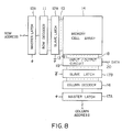
- FIG. 8 there is shown a second embodiment of this invention.
- This figure shows the circuit arrangement in the case where the address setup time t as (see FIG. 3) is shorter than the address decode time t dec (see FIG. 3).
- the latch operation on the row side is carried out by the master latch 12A and the slave latch 12B
- the latch operation on the column side is carried out by the master latch 17A and the slave latch 17B.
- a row address is applied to the memory array 14 through the master latch 12A, the row decoder 11, the slave latch 12B, and the word line 13.
- a column address serves to select a corresponding bit line 18 through the master latch 17A, the column decoder 16, the slave latch 17B, and the input/output circuit 19.
- the master latches 12A and 17A latch respectively outputs for a time period during which the synchronizing signal ⁇ is at the H level, and output respective inputs as they are for a time period during which the synchronizing signal ⁇ is at the L level.
- the slave latches 12B and 17B latch respective outputs for a time period during which the synchronizing signal ⁇ is at the H level (i.e., the synchronizing signal ⁇ is at the L level), and output respective inputs as they are for a time period during which the synchronizing signal ⁇ is at the L level (i.e. the synchronizing signal ⁇ is at the H level).
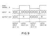
- FIG. 9 is a timing chart showing the operation of the master latches 12A, 17A.
- the latches 12A, 17A take thereinto values of its input IN (A) in response to the rise of the synchronizing signal ⁇ , and maintains its output (A) for a time period during which the synchronizing signal ⁇ is at the H level.
- the synchronizing signal ⁇ shifts to the L level
- the above-mentioned latches output respective applied inputs IN as they are.
- the synchronizing signal ⁇ shifts to the H level for a second time, they take thereinto the value of input IN (B), and maintain the value (B) for a time period during which the synchronizing signal ⁇ is at the H level.
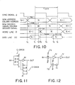
- FIG. 10 is a timing chart showing the read operation of the memory shown in FIG. 8.
- row and column addresses are defined.
- the synchronizing signal ⁇ is at the L level.
- row and column addresses (N) are passed through the master latches 12A, 17A as they are, and are then applied to the row and column decoders 11 and 16.
- decoding operation is initiated in respective decoders 11, 16.
- the synchronizing signal ⁇ shifts to the H level.
- the master latches 12A, 17A latch their outputs.
- a decoded signal (N) is outputted to the word line 13 at time t3 when the word line drive time t dr has passed, and is defined. Thereafter, at time t5 when the sense time t sense has passed, data (N) is outputted to the data line 20, and is defined. This status is continued for a setup time t ds . At time t6, the synchronizing signal ⁇ shifts to the H level. Thus, the cycle time t ⁇ cycle is completed. At times subsequent thereto, the above-mentioned operations will be repeatedly carried out.
- t ⁇ cycle t dec + t dr + t sense + t ds - t as (3)
- circuit configuration shown in FIG. 11 or 12 may be used.
- FIG. 11 is a static latch circuit using the clocked CMOS (C-CMOS) as a switch circuit.
- FIG. 12 is a static latch circuit using a transfer gate TG of the CMOS type as a switch circuit.
- FIGS. 13 and 14 show static latch circuits which comprise feedback circuits having no switch circuit (clocked CMOS or transfer gate). In these circuits, the drive forces of the feedback circuits are made to be weak, and inputs are inversed by the switch circuits of the first stages.
- respective latches 12A, 12B, 17A, 17B in FIG. 8 the circuit configurations shown in FIGS. 11 to 14 may be used.
- latches When such latches are used as the master latch, it is sufficient to apply synchronizing signals ⁇ and ⁇ to the terminals thereof as shown in respective figures.
- latches when such latches are used as the slave latch, it is sufficient to apply synchronizing signals ⁇ and ⁇ to the terminals thereof in a manner opposite to that in connection with the case of the master latch.
- the above-described respective latches are not limited to the circuit configuration shown in FIGS. 11 to 14.
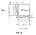
- the column system may adopt the same circuit configuration as that of the background art shown in FIG. 22. Examples where only the row system is subjected to pipe-line processing are shown in FIGS. 15 and 16, respectively.
- the circuit shown in FIG. 15 is characterized in that the same circuit configuration as that in FIG. 22 is employed as the column system in the circuit configuration shown in FIG. 1.
- the circuit shown in FIG. 16 is characterized in that the same circuit configuration as that in FIG. 22 is employed as the column system in the circuit configuration shown in FIG. 8.
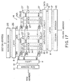
- Some large capacity static RAMs adopt the double word line structure.
- This invention is applicable to memories of such a double word line structure, thus making it possible to realize a shortened cycle time.
- a latch 12 is provided at the next stage of the row decoder 11, thus to drive main word lines MWL ⁇ , ..., MWLn .
- the memory cell array 14 is divided into several subarrays 14A, 14A, ⁇ . Selection of respective subarrays 14A is carried out by a section decoder 25. Namely, a latch 26 is provided at the next stage of the section decoder 25. Section select lines SS ⁇ , ..., SSs are driven by outputs from the latch 26.
- Word lines SWL ⁇ , ..., SWL ⁇ n, ..., SWLS ⁇ , ..., SWLSn connected to respective memory cells 27, 27, ... are output lines from NOR elements 28, 28, ..., respectively. To the respective input terminals of these NOR elements 28, 28, ..., main word lines MWL ⁇ , ..., MWLn and section select lines SS ⁇ , ..., SSs are connected.
- one NOR element 28 is selected by outputs from the latches 12, 26.
- one of the word lines SWL ⁇ n to SWLS1 ⁇ n
- the circuit configuration shown in FIG. 17 can also shorten the cycle time in the same manner as that in the circuit arrangement shown in FIG. 1.
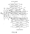
- the latch 26 shown in FIG. 17 is composed of a master latch 26A and a slave latch 26B which are shown in FIG. 18. These latches 26A, 26B are connected before and after the section decoder 25.
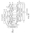
- a latch 17 may be arranged at the preceding stage of the column decoder 16 in the column system as shown in FIGS. 19 and 20 with the same relationship as the relationship between the circuit configurations shown in FIGS. 1 and 15 and the relationship between the circuit configurations shown in FIGS. 8 and 16.
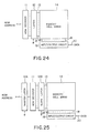
- column decoder 26 is unnecessary. In that case, it is sufficient that the circuit configuration of FIG. 18 is changed to that shown in FIG. 21.
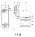
- FIGS. 27 and 28 there are shown still further embodiments of this invention where a data processing unit 30 such as a microprocessor, etc. is provided.
- a data processing unit 30 such as a microprocessor, etc.
- an address generation circuit 26 within the data processing unit 30 such as a microcomputer, etc. and row decoder 11 provided in association with the memory are interconnected through an address bus 28, and input/output circuit 19 provided in association with the memory and an input/output circuit 27 (for driving the input/output circuit 19) are interconnected through an address bus 29.
- the address generation circuit 26 within the data processing unit 30 and the address decoders 11, 16 provided in association with the memory are directly connected without intervention of latch. Accordingly, an address generated in the address generation circuit 26 within the data processing unit 30 is immediately decoded at the address decoders 11, 16.
- operation up to the address decoding can be completed by the pipe-line processing for the address generation.
- the cycle time of a large capacity memory determines the cycle time of the system. In such instances, when these embodiments are employed, it is possible to shorten the cycle time by the address decode time as compared to that of the conventional memory and without the addition of a special restriction.
- FIGS. 29 and 30 there are shown still more further embodiments of this invention where a data processing unit is provided.
- the address generation circuit 26 within the data processing unit 30 and a master latch 12A provided in association with the memory are interconnected through the address bus 28, and an input/output circuit 19 provided in association with the memory and input/output circuit 27 within the data processing unit 30 are interconnected through the data bus 29.
- address decoding can be carried out over cycles.
- a sequence comprising the steps of address generation, address decoding, and memory access can be executed in two cycles in a time as short as possible. Namely, the critical path of the system can be optimized over cycles.
Landscapes
- Engineering & Computer Science (AREA)
- Microelectronics & Electronic Packaging (AREA)
- Computer Hardware Design (AREA)
- Static Random-Access Memory (AREA)
- Dram (AREA)
- Semiconductor Memories (AREA)
Applications Claiming Priority (2)
| Application Number | Priority Date | Filing Date | Title |
|---|---|---|---|
| JP294401/88 | 1988-11-21 | ||
| JP63294401A JPH02141993A (ja) | 1988-11-21 | 1988-11-21 | 半導体記憶装置 |
Publications (2)
| Publication Number | Publication Date |
|---|---|
| EP0370460A2 true EP0370460A2 (fr) | 1990-05-30 |
| EP0370460A3 EP0370460A3 (fr) | 1991-07-24 |
Family
ID=17807261
Family Applications (1)
| Application Number | Title | Priority Date | Filing Date |
|---|---|---|---|
| EP19890121518 Withdrawn EP0370460A3 (fr) | 1988-11-21 | 1989-11-21 | Dispositif de mémoire semi-conducteur |
Country Status (4)
| Country | Link |
|---|---|
| US (1) | US5073873A (fr) |
| EP (1) | EP0370460A3 (fr) |
| JP (1) | JPH02141993A (fr) |
| KR (1) | KR930000767B1 (fr) |
Cited By (3)
| Publication number | Priority date | Publication date | Assignee | Title |
|---|---|---|---|---|
| EP0511397A4 (en) * | 1990-11-16 | 1994-07-06 | Fujitsu Ltd | Semiconductor memory having high-speed address decoder |
| EP0637132A3 (fr) * | 1993-07-30 | 1995-09-20 | Nec Corp | Circuit simple de stockage temporaire d'informations à commande par signal de validation/remise à zéro. |
| US6925028B2 (en) | 2001-03-29 | 2005-08-02 | International Business Machines Corporation | DRAM with multiple virtual bank architecture for random row access |
Families Citing this family (13)
| Publication number | Priority date | Publication date | Assignee | Title |
|---|---|---|---|---|
| US5398206A (en) * | 1990-03-02 | 1995-03-14 | Hitachi, Ltd. | Semiconductor memory device with data error compensation |
| US5799186A (en) * | 1990-12-20 | 1998-08-25 | Eastman Kodak Company | Method and apparatus for programming a peripheral processor with a serial output memory device |
| US5546561A (en) * | 1991-02-11 | 1996-08-13 | Intel Corporation | Circuitry and method for selectively protecting the integrity of data stored within a range of addresses within a non-volatile semiconductor memory |
| JP3408552B2 (ja) * | 1991-02-11 | 2003-05-19 | インテル・コーポレーション | 不揮発性半導体メモリをプログラム及び消去する回路とその方法 |
| TW294861B (fr) * | 1992-02-21 | 1997-01-01 | Siemens Ag | |
| JPH05266654A (ja) * | 1992-03-17 | 1993-10-15 | Mitsubishi Electric Corp | マルチポートメモリ装置 |
| JP3424262B2 (ja) * | 1993-04-21 | 2003-07-07 | ヤマハ株式会社 | オンライン型カラオケシステム |
| JPH07235193A (ja) * | 1993-12-28 | 1995-09-05 | Toshiba Corp | 半導体記憶装置 |
| JPH0916468A (ja) * | 1995-06-30 | 1997-01-17 | Nec Corp | メモリアクセス方式 |
| JP3630847B2 (ja) * | 1996-05-16 | 2005-03-23 | 株式会社ルネサステクノロジ | ラッチ回路 |
| US6154056A (en) * | 1997-06-09 | 2000-11-28 | Micron Technology, Inc. | Tri-stating address input circuit |
| DE19928454B4 (de) * | 1998-06-29 | 2010-01-21 | Fujitsu Microelectronics Ltd. | Speichervorrichtung mit Reihendecodierer |
| US7796464B1 (en) | 2003-06-27 | 2010-09-14 | Cypress Semiconductor Corporation | Synchronous memory with a shadow-cycle counter |
Family Cites Families (11)
| Publication number | Priority date | Publication date | Assignee | Title |
|---|---|---|---|---|
| JPS58211393A (ja) * | 1982-06-02 | 1983-12-08 | Mitsubishi Electric Corp | 半導体メモリ装置 |
| JPS5960792A (ja) * | 1982-09-30 | 1984-04-06 | Fujitsu Ltd | 半導体メモリ装置 |
| JPS5972698A (ja) * | 1982-10-18 | 1984-04-24 | Mitsubishi Electric Corp | 半導体メモリ装置 |
| JPS59155954A (ja) * | 1983-02-24 | 1984-09-05 | Mitsubishi Electric Corp | 半導体メモリ装置 |
| US4685088A (en) * | 1985-04-15 | 1987-08-04 | International Business Machines Corporation | High performance memory system utilizing pipelining techniques |
| JPS62248195A (ja) * | 1986-04-21 | 1987-10-29 | Seiko Epson Corp | 半導体記憶装置 |
| JPH0821231B2 (ja) * | 1986-08-13 | 1996-03-04 | 株式会社日立製作所 | 半導体メモリ |
| JPS63122089A (ja) * | 1986-11-12 | 1988-05-26 | Nec Corp | 半導体記憶装置 |
| JPS63225991A (ja) * | 1987-03-16 | 1988-09-20 | Hitachi Ltd | 半導体記憶装置 |
| JP2934444B2 (ja) * | 1988-03-16 | 1999-08-16 | 株式会社日立製作所 | 半導体メモリ装置 |
| JPH0291877A (ja) * | 1988-09-27 | 1990-03-30 | Nec Corp | 半導体記憶装置 |
-
1988
- 1988-11-21 JP JP63294401A patent/JPH02141993A/ja active Pending
-
1989
- 1989-11-21 KR KR1019890016964A patent/KR930000767B1/ko not_active Expired - Fee Related
- 1989-11-21 EP EP19890121518 patent/EP0370460A3/fr not_active Withdrawn
- 1989-11-21 US US07/439,870 patent/US5073873A/en not_active Expired - Fee Related
Cited By (5)
| Publication number | Priority date | Publication date | Assignee | Title |
|---|---|---|---|---|
| EP0511397A4 (en) * | 1990-11-16 | 1994-07-06 | Fujitsu Ltd | Semiconductor memory having high-speed address decoder |
| US5394373A (en) * | 1990-11-16 | 1995-02-28 | Fujitsu Limited | Semiconductor memory having a high-speed address decoder |
| EP0637132A3 (fr) * | 1993-07-30 | 1995-09-20 | Nec Corp | Circuit simple de stockage temporaire d'informations à commande par signal de validation/remise à zéro. |
| US5511034A (en) * | 1993-07-30 | 1996-04-23 | Nec Corporation | Simple temporary information storage circuit controllable with enable/reset signal |
| US6925028B2 (en) | 2001-03-29 | 2005-08-02 | International Business Machines Corporation | DRAM with multiple virtual bank architecture for random row access |
Also Published As
| Publication number | Publication date |
|---|---|
| EP0370460A3 (fr) | 1991-07-24 |
| US5073873A (en) | 1991-12-17 |
| JPH02141993A (ja) | 1990-05-31 |
| KR900008522A (ko) | 1990-06-04 |
| KR930000767B1 (ko) | 1993-02-01 |
Similar Documents
| Publication | Publication Date | Title |
|---|---|---|
| EP0370460A2 (fr) | Dispositif de mémoire semi-conducteur | |
| US6519187B2 (en) | Semiconductor memory device having read data multiplexer | |
| US6078546A (en) | Synchronous semiconductor memory device with double data rate scheme | |
| EP0056240B1 (fr) | Dispositif de mémoire | |
| JPH11191292A (ja) | 半導体記憶装置およびそのバーストアドレスカウンタ | |
| KR0154586B1 (ko) | 반도체 기억장치 | |
| JPH08279282A (ja) | 集積回路メモリ | |
| US4667310A (en) | Large scale circuit device containing simultaneously accessible memory cells | |
| JPH0896574A (ja) | 半導体記憶装置 | |
| JP2002216479A (ja) | クワッドデータレートシンクロナス半導体メモリ装置の駆動方法及び駆動回路 | |
| KR19980075585A (ko) | 동기식 반도체 메모리장치의 칼럼 선택라인 제어회로 및 제어방법 | |
| US6975151B2 (en) | Latch circuit having reduced input/output load memory and semiconductor chip | |
| JP3351643B2 (ja) | 半導体メモリ装置及びその製造方法 | |
| US6178139B1 (en) | Semiconductor memory device comprised of a double data rate-synchronous dynamic random access memory | |
| JPH0158591B2 (fr) | ||
| US6411563B1 (en) | Semiconductor integrated circuit device provided with a logic circuit and a memory circuit and being capable of efficient interface between the same | |
| KR100324143B1 (ko) | 반도체 메모리장치 및 번인 테스트 방법 | |
| EP0660328B1 (fr) | Méthode de commande d'un circuit d'emmagasinage à semi-conducteurs | |
| US6714475B2 (en) | Fast accessing of a memory device using decoded address during setup time | |
| US5701273A (en) | Memory device | |
| US6442103B1 (en) | Synchronous SRAM device with late write function | |
| US5661693A (en) | Memory device for synchronously reading and writing data | |
| US5970020A (en) | Controlling the set up of a memory address | |
| US5602782A (en) | Pipeline-operating type memory system capable of reading data from a memory array having data width larger than the output data width | |
| JP2001344977A (ja) | 半導体記憶装置 |
Legal Events
| Date | Code | Title | Description |
|---|---|---|---|
| PUAI | Public reference made under article 153(3) epc to a published international application that has entered the european phase |
Free format text: ORIGINAL CODE: 0009012 |
|
| 17P | Request for examination filed |
Effective date: 19891121 |
|
| AK | Designated contracting states |
Kind code of ref document: A2 Designated state(s): DE FR GB IT |
|
| PUAL | Search report despatched |
Free format text: ORIGINAL CODE: 0009013 |
|
| AK | Designated contracting states |
Kind code of ref document: A3 Designated state(s): DE FR GB IT |
|
| 17Q | First examination report despatched |
Effective date: 19930526 |
|
| STAA | Information on the status of an ep patent application or granted ep patent |
Free format text: STATUS: THE APPLICATION IS DEEMED TO BE WITHDRAWN |
|
| 18D | Application deemed to be withdrawn |
Effective date: 19931006 |